Note: Descriptions are shown in the official language in which they were submitted.
CA 02844156 2015-08-24
DYNAMIC STEP DIMMING INTERFACE
Inventors: Arturo Hernandez Lopez,
Markus Ziegler, and Carlos
Daniel Ortega Jaramillo
CROSS-REFERENCE TO RELATED APPLICATION
[0001] The present application claims priority of United States Provisional
Application
No. 61/774,556, filed March 7, 2013 and entitled "DYNAMIC STEP DIMMING
INTERFACE".
TECHNICAL FIELD
[0002] The present invention relates to lighting, and more specifically, to
electronics for
lighting.
BACKGROUND
[0003] A typical step dimming interface for an electronic ballast or other
lighting power
device utilizes a high-impedance network and an integrator filter to measure a
source
voltage. The step dimming interface allows the device to energize and/or
operate a
lamp connected thereto at one or more pre-determined dimming levels. The
device is
able to step between different dimming levels based on, for example, user
input.
SUMMARY
[0004] Unfortunately, a typical step dimming interface is not always robust
enough to
provide step dimming functionality in noisy environments. Frequently, these
interfaces
Page 1 of 29
CA 02844156 2014-02-27
provide diminished results because they integrate low and high frequency
noise. When
such step dimming interfaces are exposed to noise, the integrator filter is
not robust
enough to filter out the noise. Thus, a typical step dimming interface
provides a
diminished step dimming capability when exposed to noisy environments. Thus,
there
is a need for a step dimming interface that efficiently provides noise
immunity.
[0005] Embodiments of the present invention relate to a step dimming interface
that
provides robust noise immunity for dynamically operating a load, such as but
not
limited to a gas discharge lamp and/or a lamp and/or other lighting device
including
one or more solid state light sources (e.g., light emitting diodes, organic
light emitting
diodes, polymer light emitting diodes, organic light emitting compounds,
etc.). In
particular, the step dimming interface controls whether the lamp is operating
in either a
normal power mode or a dim power mode, and dynamically provides a control
command to indicate whether the lamp should operate in the normal power mode
or in
the dim power mode.
[0006] In some embodiments, the step dimming interface is a system to be used
with a
voltage source producing an oscillating current. A ballast is connected to the
oscillating
current to energize at least one lamp and includes a lamp control circuit. The
lamp
control circuit receives a mode command from the step dimming interface to
alter the
power level applied to the lamp(s) between a level corresponding to a dim mode
and a
level corresponding to a normal mode. The system includes a voltage monitor
with an
input to receive the oscillating current and an output to indicate the voltage
level of the
oscillating current. The system also includes a processing circuit that has a
first input
connected to the output of the voltage monitor, and a first output that is
connected to
the lamp control circuit. The processing circuit provides a mode command to
the
ballast (more specifically, the lamp control circuit), indicating whether the
lamp is to be
energized in a dim mode or a normal mode. The processing circuit also includes
a
second output to provide a reference voltage that is indicative of the voltage
of the
oscillating current. A rectifier circuit has an input to receive the
oscillating current and
an output to provide rectified voltage indicative of the oscillating current.
The rectifier
Page 2 of 29
CA 02844156 2014-02-27
circuit is responsive to user input that allows for selectively energizing the
lamp in a
dim mode and a normal mode. A comparator circuit has a first input connected
to the
output of the rectifier circuit, a second input connected to the processing
circuit to
receive the reference voltage therefrom, and an output connected to a second
input of
the processing circuit to provide a second voltage that is indicative of a
power applied
to the lamp(s). The processing circuit is responsive to the second voltage and
to the
voltage level output by the voltage monitor to provide the mode command.
[00071 In an embodiment, there is provided a system. The system includes: a
ballast
configured to be connected a source of an oscillating current and to energize
a lamp,
wherein the ballast comprises a lamp control circuit responsive to a mode
command
indicating whether the lamp will be energized in one of a dim mode and a
normal
mode; a voltage monitor comprising an input configured to receive the
oscillating
current and an output configured to indicate a voltage level of the
oscillating current; a
processing circuit comprising a first input connected to the output of the
voltage
monitor to receive the voltage level therefrom, a second input, a first output
connected
to the lamp control circuit to provide the mode command thereto, wherein the
mode
command indicates one of a dim mode and a normal mode, and a second output to
provide a reference voltage indicative of the voltage level of the oscillating
current; a
rectifier circuit comprising an input configured to receive the oscillating
current and an
output configured to provide a rectified voltage indicative of the oscillating
current,
wherein the rectifier circuit is responsive to user input to selectively
energize the lamp
in one of a dim mode and a normal mode; and a comparator circuit comprising a
first
input connected to the rectifier circuit, a second input connected to the
second output of
the processing circuit, and an output connected to the second input of the
processing
circuit and configured to provide a compared voltage indicative of a power
level
applied to the lamp; wherein the processing circuit is responsive to the
compared
voltage provided by the comparator circuit and is responsive to voltage level
indicated
by the voltage monitor to provide the mode command to the ballast.
Page 3 of 29
CA 02844156 2014-02-27
[0008] In a related embodiment, the rectifier circuit may include a resistive
voltage
divider circuit to limit a peak voltage of the oscillating current, and a
capacitive circuit
to remove high-frequency noise in the rectifier voltage. In a further related
embodiment, the processing circuit may average the compared voltage over a
period of
time. In a further related embodiment, the period of time may be between one
second
and four seconds.
[0009] In another related embodiment, the processing circuit may include a
time delay
between receiving the compared voltage and providing the mode command
indicating
one of a dim mode and a normal mode. In a further related embodiment, the
processing circuit may be configured to validate the user input during the
time delay.
In a further related embodiment, the processing circuit may be configured to
validate
the user input by confirming the user input during the time delay. In another
further
related embodiment, the time delay may be between one second and four seconds.
In
yet another further related embodiment, the time delay may be at least one
second.
[0010] In still another related embodiment, the comparator circuit may include
an auto-
programmable comparator circuit including an output configured to provide one
or
more pulses to the second input of the processing circuit. In a further
related
embodiment, the processing circuit may include: a central processing unit
including a
first input connected to the output of the voltage monitor, a second input, a
third input,
a first output connected to the lamp control circuit to provide a mode command
indicating that the lamp will be energize in one of a dim mode and a normal
mode, and
a second output to provide a reference voltage indicative of the voltage level
of the
oscillating current; a pulse counter including an input to receive the one or
more pulses
from the auto-programmable comparator circuit and an output connected to the
second
input of the central processing unit to provide a second voltage indicative of
the state of
the lamp controlled by the lamp control circuit; and a clock circuit including
an output
connected to the third input of the central processing unit to provide a time
reference
for the one or more pulses; wherein the central processing unit may be
responsive to the
second voltage and to the time reference to provide the mode command.
Page 4 of 29
CA 02844156 2014-02-27
[00111 In another embodiment, there is provided a system. The system includes:
a
ballast configured to be connected to a source of an oscillating current and
to energize a
lamp, wherein the ballast comprises a lamp control circuit responsive to a
mode
command indicating whether the lamp will be energized in one of a dim mode and
a
normal mode; a voltage monitor comprising an input configured to receive the
oscillating current and an output configured to indicate a voltage level of
the oscillating
current signal; a central processing circuit comprising a first input
connected to the
output of the voltage monitor, a second input, a third input, a first output
connected to
the lamp control circuit to provide a mode command indicating that the lamp
will be
energized in one of a dim mode and a normal mode, and a second output to
provide a
reference voltage indicative of the voltage level of the oscillating current;
a rectifier
circuit comprising an input configured to receive the oscillating current, an
output
configured to provide a rectified voltage indicative of the oscillating
current, a resistive
voltage divider circuit to limit a peak voltage of the oscillating current,
and a capacitive
circuit to remove high-frequency noise; an auto-programmable comparator
circuit
comprising a first input connected to the rectifier circuit, a second input
connected to
the second output of the central processing circuit, and an output configured
to provide
one or more pulses indicative of a power level applied to the lamp; a pulse
counter
comprising an input to receive the one or more pulses from the auto-
programmable
comparator circuit and an output connected to the second input of the central
processing circuit to provide a second voltage indicative of the state of the
lamp
controlled by the lamp control circuit; and a clock circuit comprising an
output
connected to the third input of the central processing circuit to provide a
time reference
for the one or more pulses; wherein the central processing circuit is
responsive to the
one or more pulses and to the voltage level output by the voltage monitor to
provide
the mode command.
[0012] In a related embodiment, the central processing circuit may average the
one or
more pulses over a period of time. In a further related embodiment, the period
of time
may be between one second and four seconds.
Page 5 of 29
CA 02844156 2014-02-27
[0013] In another related embodiment, the central processing circuit may
include a time
delay between receiving the one or more pulses and providing the mode command
indicating one of a dim mode and a normal mode. In a further related
embodiment, the
central processing circuit may be configured to validate the user input during
the time
delay by confirming the user input during the time delay. In a further related
embodiment, the time delay may be between one second and four seconds.
[00141 In another embodiment, there is provided a method of energizing a lamp
in one
of a dim mode and a normal mode. The method includes: monitoring a voltage
level of
an oscillating current; determining a reference voltage corresponding to the
voltage
level of the oscillating current; calculating whether a voltage level of a
rectified voltage
corresponding to the oscillating current is greater than a determined
reference voltage,
and in response: when the voltage level of the rectified voltage is greater
than the
determined reference voltage: verifying that the voltage level of the
rectified voltage
continues to be greater than the determined reference voltage for a period of
time; and
in response, generating a dim operating mode command for a lamp control
circuit to
place the lamp in a dim operating mode; otherwise if the voltage level of the
rectified
voltage is not greater than the determined reference voltage for any portion
of the
period of time, continuing to monitor the voltage level of the oscillating
current; when
the voltage level of the rectified voltage is not greater than the determined
reference
voltage: verifying that the voltage level of the rectified voltage continues
to be not
greater than the determined reference voltage for the period of time; in
response,
determining whether an indication exists for operating the lamp in the dim
operating
mode; wherein if the indication to operate in the dim operating mode exists,
generating
a dim operating mode command for a lamp control circuit to place the lamp in a
dim
operating mode; wherein if the indication to operate in the dim operating mode
does
not exist, generating a normal operating mode command for the lamp control
circuit to
place the lamp in a normal operating mode; otherwise, if the voltage level of
the
rectified voltage is greater than the determined reference voltage for any
portion of the
period of time, continuing to monitor the voltage level of the oscillating
current.
Page 6 of 29
CA 02844156 2014-02-27
BRIEF DESCRIPTION OF THE DRAWINGS
[0015] The foregoing and other objects, features, and advantages disclosed
herein will
be apparent from the following description of particular embodiments disclosed
herein,
as illustrated in the accompanying drawings in which like reference characters
refer to
the same parts through the different views. The drawings are not necessarily
to scale,
emphasis instead being placed upon illustrating the principles disclosed
herein.
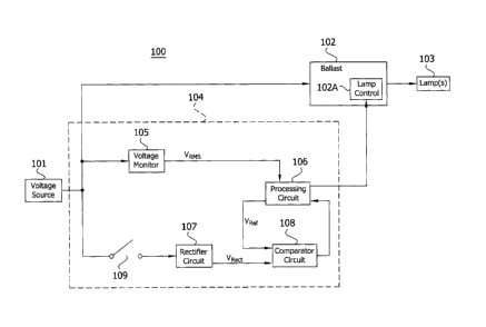
[0016] FIG. 1 is a block diagram of a system including a ballast and a step
dimming
interface according to embodiments disclosed herein.
[0017] FIG. 2 is a block diagram of a rectifier circuit of the step dimming
interface of
FIG. 1 according to embodiments disclosed herein.
[0018] FIG. 3 is a schematic diagram of a voltage divider circuit according to
embodiments disclosed herein.
[0019] FIG. 4 is a schematic diagram of a capacitive circuit according to
embodiments
disclosed herein.
[0020] FIG. 5 is a block diagram of a processing circuit of the step dimming
interface of
FIG. 1 according to embodiments disclosed herein.
[0021] FIG. 6 is a flowchart illustrating a method of operating a step dimming
interface
according to embodiments disclosed herein.
[0022] FIGs. 7-13 are waveforms illustrating functionality of the dynamic step
dimming
interface of FIGs. 1-6 according to embodiments disclosed herein.
DETAILED DESCRIPTION
[0023] FIG. 1 illustrates a step dimming interface system 100. The step
dimming
interface system 100 is for use with an input voltage source 101 that provides
an
oscillating current, such as but not limited to an alternating current (AC)
power supply.
The step dimming interface system 100 includes an electronic ballast 102 (also
referred
to throughout as the ballast 102) to energize at least one lamp 103 and a step
dimming
Page 7 of 29
CA 02844156 2014-02-27
interface 104 that validates the dim mode, providing higher immunity in noisy
environments. In some embodiments, the ballast 102 is an outdoor electronic
ballast
capable of operating between 0 and 10 volts and includes a step dimming
feature. In
other embodiments, the ballast 102 is used in street lighting applications to
operate gas
discharge lamps, such as but not limited to metal-halide lamps and/or high-
pressure
sodium lamps, or in other lighting applications to operate low pressure gas
discharge
lamps. In other embodiments, the ballast 102 is the current-limiting resistor
(also
known as a ballast resistor) of a driver for a lighting device including one
or more solid
state light sources. In some embodiments, the lamp(s) 103 are fluorescent
lamps, while
in some embodiment, the lamp(s) 103 are lighting devices including one or more
solid
state light sources. However, it is contemplated that other types of lamps may
be used
as well.
[0024] The ballast 102 includes a voltage input port adapted for connecting to
the
voltage source 101 and an output port that connects to the lamp(s) 103. The
ballast 102
also includes a lamp control circuit 102A, which receives a mode command from
a
processing circuit 106 for altering the power level applied to the lamp(s) 103
between a
level corresponding to a dim operating mode and a level corresponding to a
normal
operating mode. In some embodiments, power applied to the lamp(s) 103 in the
dim
operating mode may be 30% to 70% of the power applied in the normal operating
mode.
[0025] The step dimming interface 104 is responsive to user input to control
when the
lamp(s) 103 operates in either a normal mode or a dim mode. The step dimming
interface 104 is a low-cost step dimming interface that efficiently improves
the noise
immunity for universal voltage electronic dimmable ballasts or universal LED
dimmable drivers. In contrast to noise-susceptible interfaces that use a high
impedance
network and an integrator filter to measure the average voltage, the step
dimming
interface 104 is more robust in noisy environments. The step dimming interface
104
includes a voltage monitor 105, a processing circuit 106, a rectifier circuit
107, a
comparator circuit 109, and a user input port 109.
Page 8 of 29
CA 02844156 2014-02-27
[0026] The voltage monitor 105 includes a voltage input port adapted for
connecting to
the voltage source 101 for receiving and monitoring the oscillating current.
The voltage
monitor 105 has an output port providing a voltage level that is the voltage
level of the
monitored oscillating current. For example, in some embodiments, the voltage
monitor
105 is an analog to digital converter voltage monitor available from as part
of a
microcontroller or as a stand alone component. In some embodiments, the
voltage level
that is provided by the voltage monitor 105 is the root mean square (RMS)
value of the
oscillating current signal generated by the voltage source 101. Thus, the
voltage
monitor 105 measures the voltage level of the voltage source 101 and generates
a
corresponding voltage level VRMS indicative of the measured voltage level.
[0027] The rectifier circuit 107 includes a voltage input port adapted for
connecting to
the voltage source 101 for receiving the oscillating current and an output
port connected
to a comparator circuit 108. The output port of the rectifier circuit 107
provides a
rectified voltage VRect indicative of the oscillating current to the
comparator circuit 108.
The user input port 109 is adapted to be connected between the voltage source
101 and
the rectifier circuit 107. The user input port 109 receives user input that
indicates if the
lamp(s) 103 are to be selectively energized at a dimmed power level or at the
normal
power level. Thus, the rectifier circuit 107 is responsive to user input for
selectively
energizing the lamp(s) 103 in either a dim mode or a normal mode. In some
embodiments, the user input port 109 is a switch. The rectifier circuit 107
receives the
oscillating current from the voltage source 101 when the switch is closed by
the user
and provides a corresponding rectified voltage VRect. In some embodiments, the
corresponding rectified voltage VRect is a half-wave rectified voltage.
[0028] The processing circuit 106 is connected to the output port of the
voltage monitor
105 and to the output port of the comparator circuit 108, and this includes
two inputs.
The processing circuit 106 is also connected to an input port of the
comparator circuit
108 and the input port of the lamp control circuit 102A, and thus includes two
outputs.
In some embodiments, the processing circuit 106 is a microcontroller or a
Page 9 of 29
CA 02844156 2014-02-27
microprocessor. In some embodiments, the processing circuit 106 is a ballast
for a gas
discharge lamp or a controller for driver for one or more solid state light
sources.
[0029] The comparator circuit 108 includes a first voltage input port
connected to the
rectifier circuit 107, a second voltage input port connected to the processing
circuit 106,
and a voltage output port connected to the processing circuit 106. In some
embodiments, the comparator circuit 108 is an internal comparator, while in
other
embodiments, the comparator circuit 108 is an external comparator, available
from a
microcontroller, such as but not limited to the AT9OPWM81, as a peripheral.
The
comparator circuit 108 receives the rectified voltage VRect from the rectifier
circuit 107
and the reference voltage VRef from the processing circuit 106 and compares
the voltage
levels of these. When the rectified voltage VRect is greater than the
reference voltage VRef,
the comparator circuit 108 generates a compared voltage at a first level. When
the
rectified voltage VRect is less than the reference voltage VRef, the
comparator circuit
generates a compared voltage at a second level, such that the change in levels
appears
to be a pulse. FIGs. 7-13 include waveforms illustrating the dynamic step
dimming
interface functionality.
[0030] In some embodiments, the compared voltage generated by the comparator
circuit
108 is a square wave, that is, a sequence of one or more pulses. The
processing circuit
106 receives the one or more pulses and when a number of pulses are
accumulated over
a certain period of time corresponding to a preset period of time, the
processing circuit
106 produces a command indicating to the lamp control circuit 102A that the
lamp(s)
103 should be placed at the dimming power level (i.e., enter the dim operating
mode).
For example, if the frequency of the one or more pulses is 20 Hz, and the
preset period
of time is two seconds, 40 received pulses would cause the processing circuit
106 to
produce a command indicating to the lamp control circuit 102A that the lamp(s)
103
should be placed at the dimming power level. An absence of pulses over a
certain
period of time, e.g., less than 40 pulses in two seconds, the processing
circuit 106
produces a command indicating to the lamp control circuit 102A that the
lamp(s) 103
should be placed in the normal power mode. Thus, the command from the
comparator
Page 10 of 29
CA 02844156 2014-02-27
circuit 108 is digitally validated by the processing circuit 106 to verify
whether or not
operator input has been provided to change the operating mode of the lamp(s)
103.
This validation is accomplished by creating a time delay between the first
indication of
a mode change request and the generation of a mode command to the lamp control
circuit 102A. The validation delay period confirms the user input during the
time delay
and/or prevents an erroneous mode change from occurring due to induced noise
on the
step dimming interface 104, an intermittent voltage source connection,
variations in the
voltage source 101, or combinations thereof. In some embodiments, the default
operating mode of the lamp(s) 103 is the normal operating mode, and in some
embodiments, the default operating mode of the lamp(s) 103 is another
operating mode.
[0031] FIG. 2 illustrates the rectifier circuit 107 of FIG. 1, configured to
produce the
rectified voltage VRect in greater detail. In FIG. 2, the rectifier circuit
107 utilizes a
voltage divider circuit 201 and a capacitive circuit 202 to produce the
rectified voltage
VRect= In contrast to using a transformer, the voltage divider circuit 201
provides a low-
cost device to reduce the oscillating current from the voltage source 101 of
FIG. 1 for use
by the step dimming interface 104 of FIG. 1.
[0032] FIG. 3 shows the voltage source 101, the input port 109, and the
rectifier circuit
107, including the voltage divider circuit 201 in greater detail, and the
capacitive circuit
202. In FIG. 3, the voltage divider circuit 201 is comprised of at least three
resistors R1,
R2, R3 connected in series between the input port 109 and ground, with the
capacitive
circuit 202 connected between the resistor R2 and the resistor R3. In some
embodiments, the nominal values of the three resistors R1, R2, R3 are, for
example, 220
kiloohms (k0), 220 kn, and 2.2 kn. The actual values of the three resistors
R1, R2, R3
may, and in some embodiments does, vary as much as 5%, and thus give rise to
minimum and maximum values. Table 1 below indicates, through exemplary values,
that this variance in resistive values does not alter the selection of the
appropriate
reference voltage VRef level, as explained in greater detail below.
Page 11 of 29
CA 02844156 2014-02-27
VRMS: 108 120 220 277 305
R1 R2 R3 (k0) -
(k0) (M.))
Minimum 231 231 2.09 0.688 0.764 1.40
1.764 1.942
Nominal 220 220 2.20 0.760 0.844 1.55 1.949 2.146
Maximum 209 209 2.31 0.839 0.933 1.70 2.153 2.371
VRef: 0.4 0.4 0.8 1.6 1.6
[0033] Table 1
[0034] FIG. 4 shows the rectifier circuit 107, including the voltage divider
circuit 201 and
the capacitive circuit 202 in greater detail, along with the comparator
circuit 108. The
capacitive circuit 202 of FIG. 4 is comprised of a diode D1 connected in
parallel with a
capacitor Cl, and the parallel combination of the diode D1 and the capacitor
Cl
connected in series with a resistor R9. The voltage divider circuit 201 is
also connected
to the resistor R9, and the comparator circuit 108 is connected between the
resistor R9
and the parallel combination of the diode D1 and the capacitor Cl. The
capacitive
circuit 202 functions as a protection against voltage surges as well as a
filter to remove
unwanted noise at high frequencies.
[0035] FIG. 5 illustrates the processing circuit 106 in greater detail. In
FIG. 5, the
processing circuit 106 utilizes a central processing unit 501, a pulse counter
502, and a
clock circuit 503. In some embodiments, the central processing unit 501 is a
microprocessor or a microcontroller. The pulse counter 502 is used to count
the number
of pulses present in the one or more pulses generated by the comparator
circuit 108.
The clock circuit is used to provide a reference time in which to measure the
pulses, or
lack of pulses, in the one or more pulses generated by the comparator circuit
108.
[0036] The central processing unit 501 receives the voltage level VRMS from
the voltage
monitor 105 and calculates a peak voltage Vneak of the oscillating current
generated by
the voltage source 101, such as but not limited to by multiplying the voltage
level VRMS
Page 12 of 29
CA 02844156 2014-02-27
by a factor (e.g., the square root of two). Using the calculated peak voltage
Vpeak, the
central processing unit 501 determines the reference voltage level VRef, which
is
provided to the comparator circuit 108. The comparator circuit 108 also
receives the
rectified voltage VRect from the rectified circuit 107. In embodiments where
the rectifier
circuit 107 includes a voltage divider 201 as shown in FIG. 3, VRect may be
determined
by the central processing unit 501 by using the following formula: VRect =
(R3/(R1+R2+R3))(Vpeak). The processing circuit 106 need not calculate VRect.
Instead,
this calculation may be made during analysis by the fabricators of the system
100 and
used to calculate Vrect over a universal range (e.g., 120V - 277V) to therein
determine the
logic to be used for deciding what the reference voltage Vref should be.
[0037] Using the voltage level VRmS output by the voltage monitor 105, the
central
processing unit 501 determines the reference voltage VRef corresponding to the
received
rectified voltage VRect. In some embodiments, the central processing unit 501
selects
from a number of programmable reference voltage VRef levels stored in a memory
(not
shown in FIG. 5) that is part of, or external to and in communication with,
the central
processing unit 501. In some embodiments, the programmable reference voltage
VRef
levels are 0.4 V, 0.8 V, 1.2 V, and 1.6 V, and the central processing unit 501
selects a
reference voltage VRef that is in close proximity to, but not greater than,
the calculated
peak voltage VPeak of the oscillating current of the voltage source 101. For
example, if
the voltage level VRms is 110 V, the calculated peak voltage Vpeak will be
155.6 V, and the
rectified voltage VRect will be 0.77 V, which is the peak of a half-wave
rectified signal.
[0038] The central processing unit 501 will then select a reference voltage
VRef of 0.4 V.
Table 2 illustrates one example of the relationship among various voltage
levels VRMS,
peak voltages VPeak, and rectified voltages VRect with the four reference
voltage VRef
levels highlighted.
Page 13 of 29
CA 02844156 2014-02-27
VRms (V) Vpeak (V) VRect(V)
55 77.8 0.39
58 82.0 0.41
60 84.9 0.42
70 99.0 0.49
80 113.1 0.56
90 127.3 0.63
100 141.4 0.70
110 155.6 0.77
115 162.6 0.81
120 169.7 0.84
130 183.8 0.91
150 212.1 1.06
160 226.3 1.13
170 240.4 1.20
180 254.6 1.27
208 294.2 1.46
220 311.1 1.55
228 322.4 1.60
230 325.3 1.62
240 339.4 1.69
250 353.6 1.76
260 367.7 1.83
270 381.8 1.90
277 391.7 1.95
305 431.3 2.15
[0039] Table 2
Page 14 of 29
CA 02844156 2014-02-27
[0040] In some embodiments, the reference voltage VRef levels are selected
according to
hexadecimal values entered into registers (i.e., memory) within the processing
circuit
106. Table 3 illustrates an examples of such hexadecimal values and the
corresponding
reference voltage VRef levels.
Processing Circuit
Register Value Internal Divider VRef (V)
Internal VRef (V)
2.56 88 Internal VRef / 6.4 0.40
2.56 89 Internal VRef / 3.2 0.80
2.56 8A Internal VRef / 2.13 1.20
2.56 8B Internal VRef / 1.60 1.60
[0041] Table 3
[0042] Table 3 may be implemented by a programming routine, such as:
[0043] IF Vrms > 240, THEN Select 8B (1.6), ELSE
[0044] IF Vrms > 180, THEN Select 8A (1.20), ELSE
[0045] IF Vrms > 120, THEN Select 89 (0.8), ELSE
[0046] Select 88 (0.4).
[0047] A dedicated comparator control register is configured to set up the
internal
reference voltage. The division values are fixed and depend on the
microcontroller
type being used, such as but not limited to the AT9OPWM81 microcontroller from
ATMEL. The division values are selected by changing three binary bits in the
comparator control register.
[0048] A flowchart is shown in FIG. 6. The rectangular and diamond elements
are
herein denoted "processing blocks" and represent computer software
instructions or
groups of instructions. Alternatively, the processing blocks represent steps
performed
by functionally equivalent circuits such as a microprocessor, microcontroller,
digital
Page 15 of 29
CA 02844156 2014-02-27
signal processor circuit, or an application specific integrated circuit
(ASIC), or in
embodiments described herein, by the processing circuit 106 and its related
components. The flowcharts do not depict the syntax of any particular
programming
language. Rather, the flowcharts illustrate the functional information one of
ordinary
skill in the art requires to fabricate circuits or to generate computer
software to perform
the processing required in accordance with the present invention. It should be
noted
that many routine program elements, such as initialization of loops and
variables and
the use of temporary variables are not shown. It will be appreciated by those
of
ordinary skill in the art that unless otherwise indicated herein, the
particular sequence
of steps described is illustrative only and may be varied without departing
from the
spirit of the invention. Thus, unless otherwise stated, the steps described
below are
unordered, meaning that, when possible, the steps may be performed in any
convenient
or desirable order. More specifically, FIG. 6 illustrates a method of
operations
performed by the processing circuit 106.
[0049] As described above and below, the operations may be, and in some
embodiments are, computer program code and/or instructions stored within the
processing circuit 106 and/or external thereto, that, when executed within the
processing circuit 106, cause the system to perform the operations described
herein.
The processing circuit 106 first selects the reference voltage VRef level at
602. Next, the
processing circuit receives at 604 the one or more pulses generated by the
comparator
circuit 108 to determine whether a pulse event occurs. A pulse event occurs
when the
comparator circuit 108 generates one or more pulses that changes between two
levels,
as described above. If there are one or more pulses, the processing circuit
106 during a
time delay counts the one or more pulses as indicated by steps 606 in order to
determine whether the user input indicates a dimming operation mode for the
lamp(s)
103. If there is an absence of one or more pulses, the processing circuit 106
during a
time delay measures the absence of pulses as indicated by steps 608 in order
to
determine whether the user input indicates a normal operating mode for the
lamp(s)
103.
Page 16 of 29
CA 02844156 2014-02-27
[0050] In some embodiments, the operation of the processing circuit 106 is
implemented
by a memory and a processor executing processor executable instructions stored
in the
memory. The instructions first monitor the voltage level VRMS produced by the
voltage
monitor 105 that corresponds to the voltage level of the oscillating current.
Next, the
instructions determine which programmable reference voltage VRef level
corresponds to
the monitored voltage level VRMS, as indicated by step 602. A comparison
determines
whether the rectified voltage VRect is greater than the determined reference
voltage VRef,
as indicated by step 604. If the rectified voltage VRect is greater than the
determined
reference voltage VRef, as indicated by steps 606, then the processor waits a
period of
time to ensure that the rectified voltage VRect stays greater than the
determined
reference voltage VRef for the entire period of time. If the rectified voltage
VRect is
greater than the reference voltage VRef for the entire period of time, then
the processing
circuit 106 (which includes the processor and the memory, or is otherwise
connected to
the memory) generates a mode command indicating to the lamp control circuit
102A
that the lamp(s) 103 should be energized in the dim mode. However, if the
rectified
voltage VRect becomes less than the reference voltage VRef at some point
during the
period of time, then the processor restarts the monitoring process. If
initially, the
rectified VRect is not greater than the reference voltage VRef, as indicated
by steps 608,
then the processor waits a period of time to ensure that the reference voltage
VRef stays
greater than the rectified VRect for the entire period of time. If the
reference voltage VRef
stays greater than the rectified voltage VRect for the entire period of time,
then the
processor determines whether there is any indication that the lamp(s) 103
should be
energized in the dim mode. If there is an indication that the lamp(s) 103
should be
energized in the dim mode, then the processor executes the instructions
corresponding
to the situation where the rectified voltage VRect is greater than the
reference voltage
VRef, as described above. If there is not an indication that the lamp(s) 103
should be
energized in the dim mode, then the processing circuit 106 generates a mode
command
indicating to the lamp control circuit 102A that the lamp(s) 103 should be
energized in
the normal mode. If the rectified voltage VRect becomes greater than the
reference
Page 17 of 29
CA 02844156 2014-02-27
voltage VRef at some point during the period of time, then the processor
restarts the
monitoring process.
[0051] FIGs. 7-13 are waveforms illustrating the functionality of the dynamic
step
dimming interface of FIGs. 1-6.
[0052] More particularly, FIGs. 7-9 are snapshots of waveforms 700a, 700b,
800a, 800b,
900a, 900b illustrating what occurs when the comparator circuit 108 receives a
reference
voltage Vref from the processing circuit 106 and a rectified voltage Vrect
from the
rectifier circuit 107, depending on the voltage level Vrms output by the
voltage monitor
105, showing in detail the operation of the dynamic step dimming interface.
[0053] In FIG. 7, the waveform 700a has a voltage level Vrms of 120 Vrms,
while the
waveform 700b has a voltage level Vrms of 140 Vrms, respectively. Both of
these are
above a threshold value of the reference voltage Vref, which is 0.4 V. An
output signal
Vp of the comparator circuit 108 is a square pulse waveform that is input to a
pulse
counter, such as but not limited to the pulse counter 502 of FIG. 5. A peak of
the output
signal Vp is greater than a peak of the rectified voltage Vrect in both
waveforms 700a,
700b. Similarly, in FIG. 8, the waveform 800a has a voltage level Vrms of 220
Vrms,
while the waveform 800b has a voltage level Vrms of 260 Vrms, respectively,
which are
again both above a threshold value of the reference voltage Vref, which is 0.8
V.
However, in FIG. 8, while a peak of the output signal Vp is greater than a
peak of the
rectified voltage Vrect in the waveform 800a, the peak of the rectified
voltage Vrect is
greater than the peak of the output signal Vp in the waveform 800b.
[0054] In FIG. 9, the waveform 900a has a voltage level Vrms of 260 Vrms, and
the
waveform 900b has a voltage level Vrms of 277 Vrms, which are both above a
threshold
value of the reference voltage Vref, which is substantially 1.6V. In the
waveforms 900a
and 900b, the output signal Vp has a peak value corresponding to the reference
voltage
Vref, and the rectified voltage Vrect exceeds this peak value.
[0055] FIGs. 10 and 11 are snapshots of waveforms 1000, 1100 illustrating the
response
of the dynamic step dimming interface versus voltage transitions, more
particularly
when there is an increase, potentially a sudden increase, in the voltage
transition.
Page 18 of 29
CA 02844156 2014-02-27
Voltage transitions are fixed from low to high (emulating a sudden rising
voltage). In
the waveform 1000, pulses Vp output by the comparator 106 are not lost,
because the
reference voltage Vref is below the rectified voltage Vrect, which transitions
due to the
change in the voltage level Vrms from 120 Vrms to 220 Vrms. The processing
circuit
106 adjusts the reference voltage Vref from a threshold value of 0.4V (which
is the
reference voltage Vref divided by 6.4) to a threshold value of 1.2V (which is
the
reference voltage Vref divide dby 2.13) when the line input voltage goes from
120 Vrms
to 220 Vrms. Similarly, FIG. 11 shows the waveform 1100 having a change in
reference
voltage Vref when the lien input voltage goes from 220 Vrms to 270 Vrms, with
a
corresponding change in the rectified voltage Vrect.
[0056] FIGs. 12 and 13 detail events due to sag voltage line conditions. In
FIG. 12, a
snapshot 1200a on the left shows what happens when the lost pulse counter 604
is not
implemented. The lost pulse counter 604 avoids false triggering despite the
sag voltage
line condition. A snapshot 1200b on the right shows how the lost pulse counter
604
logic works. An oscillating waveform Vosc is related to the current on the
lamp. In
FIG. 12, the oscillating waveform Vosc in the snapshot 1200a shows the
interface
reverting back to a full power condition due to a false triggering detection.
The
oscillating waveform Vosc in the snapshot 1200b shows immunity to the
transition,
resulting in a true step dimming validation. Note that in both the snapshot
1200a and
the snapshot 1200b, the voltage transitions from 277 Vrms to 108 Vrms and back
to 277
Vrms.
[0057] The sag voltage event illustrated in the waveforms 1300a, 1300b of FIG.
13 show
how the processing circuit 106 automatically adjusts the reference voltage
Vref when
the line voltage (Vrms) changes from a high voltage level (277 Vrms) to a low
voltage
level (120 Vrms) and back again. The reference voltage Vref changes from 1.6 V
to 0.8V
and finally to 0.4 V, which in some embodiments is an optimal level.
[0058] The methods and systems described herein are not limited to a
particular
hardware or software configuration, and may find applicability in many
computing or
processing environments. The methods and systems may be implemented in
hardware
Page 19 of 29
CA 02844156 2014-02-27
or software, or a combination of hardware and software. The methods and
systems
may be implemented in one or more computer programs, where a computer program
may be understood to include one or more processor executable instructions.
The
computer program(s) may execute on one or more programmable processors, and
may
be stored on one or more storage medium readable by the processor (including
volatile
and non-volatile memory and/or storage elements), one or more input devices,
and/or
one or more output devices. The processor thus may access one or more input
devices
to obtain input data, and may access one or more output devices to communicate
output data. The input and/or output devices may include one or more of the
following: Random Access Memory (RAM), Redundant Array of Independent Disks
(RAID), floppy drive, CD, DVD, magnetic disk, internal hard drive, external
hard drive,
memory stick, or other storage device capable of being accessed by a processor
as
provided herein, where such aforementioned examples are not exhaustive, and
are for
illustration and not limitation.
[0059] The computer program(s) may be implemented using one or more high level
procedural or object-oriented programming languages to communicate with a
computer system; however, the program(s) may be implemented in assembly or
machine language, if desired. The language may be compiled or interpreted.
[0060] As provided herein, the processor(s) may thus be embedded in one or
more
devices that may be operated independently or together in a networked
environment,
where the network may include, for example, a Local Area Network (LAN), wide
area
network (WAN), and/or may include an intranet and/or the internet and/or
another
network. The network(s) may be wired or wireless or a combination thereof and
may
use one or more communications protocols to facilitate communications between
the
different processors. The processors may be configured for distributed
processing and
may utilize, in some embodiments, a client-server model as needed.
Accordingly, the
methods and systems may utilize multiple processors and/or processor devices,
and
the processor instructions may be divided amongst such single- or multiple-
processor/ devices.
Page 20 of 29
CA 02844156 2014-02-27
[0061] The device(s) or computer systems that integrate with the processor(s)
may
include, for example, a personal computer(s), workstation(s) (e.g., Sun, HP),
personal
digital assistant(s) (PDA(s)), handheld device(s) such as cellular
telephone(s) or smart
cellphone(s), laptop(s), handheld computer(s), or another device(s) capable of
being
integrated with a processor(s) that may operate as provided herein.
Accordingly, the
devices provided herein are not exhaustive and are provided for illustration
and not
limitation.
[0062] References to "a microprocessor" and "a processor", or "the
microprocessor" and
"the processor," may be understood to include one or more microprocessors that
may
communicate in a stand-alone and/or a distributed environment(s), and may thus
be
configured to communicate via wired or wireless communications with other
processors, where such one or more processor may be configured to operate on
one or
more processor-controlled devices that may be similar or different devices.
Use of such
"microprocessor" or "processor" terminology may thus also be understood to
include a
central processing unit, an arithmetic logic unit, an application-specific
integrated
circuit (IC), and/or a task engine, with such examples provided for
illustration and not
limitation.
[0063] Furthermore, references to memory, unless otherwise specified, may
include one
or more processor-readable and accessible memory elements and/or components
that
may be internal to the processor-controlled device, external to the processor-
controlled
device, and/or may be accessed via a wired or wireless network using a variety
of
communications protocols, and unless otherwise specified, may be arranged to
include
a combination of external and internal memory devices, where such memory may
be
contiguous and/or partitioned based on the application. Accordingly,
references to a
database may be understood to include one or more memory associations, where
such
references may include commercially available database products (e.g., SQL,
Informix,
Oracle) and also proprietary databases, and may also include other structures
for
associating memory such as links, queues, graphs, trees, with such structures
provided
for illustration and not limitation.
Page 21 of 29
CA 02844156 2014-02-27
[0064] References to a network, unless provided otherwise, may include one or
more
intranets and/or the internet. References herein to microprocessor
instructions or
microprocessor-executable instructions, in accordance with the above, may be
understood to include programmable hardware.
[0065] Unless otherwise stated, use of the word "substantially" may be
construed to
include a precise relationship, condition, arrangement, orientation, and/or
other
characteristic, and deviations thereof as understood by one of ordinary skill
in the art,
to the extent that such deviations do not materially affect the disclosed
methods and
systems.
[0066] Throughout the entirety of the present disclosure, use of the articles
"a" and/or
"an" and/or "the" to modify a noun may be understood to be used for
convenience and
to include one, or more than one, of the modified noun, unless otherwise
specifically
stated. The terms "comprising", "including" and "having" are intended to be
inclusive
and mean that there may be additional elements other than the listed elements.
[0067] Elements, components, modules, and/or parts thereof that are described
and/or
otherwise portrayed through the figures to communicate with, be associated
with,
and/or be based on, something else, may be understood to so communicate, be
associated with, and or be based on in a direct and/or indirect manner, unless
otherwise stipulated herein.
[0068] Although the methods and systems have been described relative to a
specific
embodiment thereof, they are not so limited. Obviously many modifications and
variations may become apparent in light of the above teachings. Many
additional
changes in the details, materials, and arrangement of parts, herein described
and
illustrated, may be made by those skilled in the art.
Page 22 of 29