Note: Descriptions are shown in the official language in which they were submitted.
CA 02844341 2014-01-10
WO 2013/008145 PCT/1B2012/053414
Modular illuminating tile
The invention relates to a modular illuminating tile comprising carrier means,
at least
one illuminating element mounted on the carrier means, means powering the
illuminat-
ing element, and a protective cover associated with the illuminating element.
The pro-
posed illuminating tile can be used primarily as decorative cover at places
exposed to
weather conditions, i.e. outdoors, at pools etc.
Utility model DE 2020 16 510 Ul discloses a tile comprising an illuminating
decoration
composed of light-emitting diodes (LEDs). The LEDs are led through holes made
in the
tile from the rear side of the tile, to form a point-like decoration on the
front side of the
tile. The wiring of the LEDs is realised on the rear side of the tile; the
solution does not
expressly provide for water-tightness or resistance to humidity.
Utility model DE 203 14 228 Ul discloses an illuminated tile, whereas the tile
is made
of transparent or translucent material at least partly on its upper side, and
it has at least
one zone at its edges where LEDs are disposed as light sources, and the light
of the
LEDs is conducted by the transparent or translucent material of the tile. Lest
the LEDs
should appear as disturbing light sources for an observer, there is a non-
transparent
frame along the edge of the tile. The description confirms that by "tile" it
means the
widest possible array of materials, and the LEDs are electrically linked and
connected
along the rear side of the tile.
Patent specification DE 10 2005002783 Al discloses an illuminated glass tile.
The de-
scription rates as disadvantageous the previously known solutions where
illumination is
provided directly by light sources fastened in the tiles, and deems it more
useful and
aesthetic to emit the light of the light sources on the surface of the tile,
instead of mak-
ing point-like light sources visible. It proposes as a solution a tile made of
transparent or
semi-transparent material, preferably of glass, with a sandwich-like
structure: the light
sources are disposed behind the glass plate at a distance secured by a
distance piece, and
the printed board carrying the light sources, the distance pieces and the
glass plate are
clamped together so as to form a single unit. Of course, this solution results
in a struc-
ture which is inevitably thicker than a normal tile.
Utility model DE 20 2004020281 Ul relates to an illuminating system comprising
a
cover plate and an illuminating element, with a printed circuit board fixed on
the rear
side of the wall or floor tile extending beyond the edge of the tile laterally
and contain-
CA 02844341 2014-01-10
WO 2013/008145 PCT/1B2012/053414
- 2 -
ing one or several light sources on the extending part.
Patent specification EP 1 268 953 B1 discloses a wall or floor tile made of
ceramics,
wood, plastic, natural or agglomerated stone comprising light-conducting and -
emitting
units, and light is supplied to these units by optical fibres. This solution
focuses first and
foremost on the placement, introduction of the optical fibres, with an eye on
the fact that
fibre optical illuminating had already been used by others.
Patent specification EP 1 469 141 B1 discloses a tile comprising a light
source. Accord-
ing to the description, the tile is suitable for forming larger patterns in
combination with
other tiles. LED is proposed as illuminating element and as light source; it
is located in
the structure of the tile, and according to the description it can installed
from the rear,
from the front or from the side, from the edge of the tile. The illuminating
structure
causes less than 3 mm extra thickness; the electrical connections are arranged
and made
primarily on the back side of the tile.
Patent specification US 7,358,929 B2 discloses tile illuminating systems and
tile illumi-
nating methods. In this solution, the light sources installed in the tile are
controlled by a
micro-computer unit which operates the integrated light sources based on a
program or
on external control.
Patent specification US 2009/0162593 Al discloses a mosaic whereas the
individual
mosaic elements are mounted so as to be spaced from one another by joints, and
the
light of a remote light souirce is transmitted to the joints by optical
fibres.
Patent specification US 2007/0103902 al discloses an illuminating fixture
comprising
LEDs on a printed circuit board mounted on the rear plane; a fully or partly
translucent
external plate in front of the LEDs, in a position secured by a distance
piece, which
closes the internal space of the fixture this way. According to this solution,
the internal
space may be empty, but the LEDs may be filled even fully with a translucent
and light-
transmitting material such as e.g. resin. The aim of this solution is, among
other things,
to display of various signs, decorations for the viewer.
Patent specification WO 2009/017629 Al discloses a decorative illuminating
tile com-
prising LED light sources fitted into the peripheral zone of the bottom layer
of a box-
like tile structure comprising several layers, hence the corner zones of the
decorative tile
v PCT/IB 2012/053 414 -
27-07-2013
CA 02844341 2014-01-10
=
-3 -
emit stronger light than the rest, which is worthy of attention considering
the light de-
sign criteria. _____________________ Gki>e/ri p ova- Zat-
f
A , ; ==_= o- _==== ma
.I= =
above by way of examples only, currently, there is no illuminating tile in the
mar -t
available in sizes and with characteristics similar to the traditional ceramic
tile- which
could be used indoors or outdoors so as to generate a random or program r ed
light ef-
fect. The aim of the proposed solution is, on the one hand, to overco = the
above defi-
ciency. The aim is, furthermore, to develop an illuminating tile = ' a modular
structure,
implying, on the one hand, the easy fitting, also in the mec = =cal sense, of
the units to
each other and, on the other, the possibility of connect' == in series beyond
the possibil-
ity of mechanical fitting, so as to make any creativ; visual appearance to be
realised by
the illuminating tiles feasible.
In an aspect of the invention this goa is realised by a modular illuminating
tile
comprising a carrier board; at least o = - illuminating element fixed on the
carrier board;
means supplying energy to the i inating element, a protective cover
associated with
the illuminating element, c = . acterised in that the at least one
illuminating element is
fixed by soldering on e carrier board; the means supplying energy to the at
least one
illuminating ele = - nt comprises electric wiring, which is connected to at
least one
electrical c= ecting means fixed mechanically on the carrier board, the at
least one
co ==cling means is fixed on the carrier board so as to permit mechanical and
- = t ' . ''' = : - : : = = .= == =
; = = .
In a preferred embodiment of the illuminating tile according to the invention
the carrier
board comprises a printed circuit board.
In a further preferred embodiment of the illuminating tile according to the
invention the
illuminating element comprises a light-emitting element.
In a further preferred embodiment of the illuminating tile according to the
invention the
illuminating element comprises an active light-emitting element.
In a further preferred embodiment of the illuminating tile according to the
invention the
illuminating element comprises a light-reflecting element.
In a further preferred embodiment of the illuminating tile according to the
invention the
REPLACEMENT SHEFTENDED SHEET
2013.07.19.
AM
PCT/IB 2012/053 414 - 27-07-2013
CA 02844341 2014-01-10
=
- 3a -
WO 2011/036614 describes a floor covering system with a PVC-based floor
covering
and a lighting system arranged to generate light. The PVC-based floor covering
has a
user side and an opposite back side. The lighting system is arranged at the
back side of
the PVC-based floor covering. The PVC-based floor covering has a light
transmission
for light generated by the lighting system in the range of 0.5% to 30%. The
PVC-based
material of the external protective cover is unprotected against external
mechanical and
environmental impacts (dirt, water, humidity, sunshine, etc.) and has physical
and
thermal characteristics that most often differ from the characteristics of the
surrounding
construction elements. This requires special handling in course of planning,
implementing and maintenance.
As can be seen from the embodiments of the currently known technical level
presented
above by way of examples only, currently, there is no illuminating tile in the
market
available in sizes and with characteristics similar to the traditional ceramic
tiles which
could be used indoors or outdoors so as to generate a random or programmed
light ef-
fect. The aim of the proposed solution is, on the one hand, to overcome the
above defi-
ciency. The aim is, furthermore, to develop an illuminating tile of a modular
structure,
implying, on the one hand, the easy fitting, also in the mechanical sense, of
the units to
each other and, on the other, the possibility of connection in series beyond
the possibil-
ity of mechanical fitting, so as to make any creative visual appearance to be
realised by
the illuminating tiles feasible.
In an aspect of the invention this goal is realised by a modular illuminating
tile
according to the features of claim 1.
REPLACEMENT SHEFTENDED SHEET
2013.07.19.
AM
CA 02844341 2014-01-10
WO 2013/008145 PCT/1B2012/053414
- 4 -
means supplying energy comprises a layer or wiring made of electrically
conductive
material.
In a further preferred embodiment of the illuminating tile according to the
invention the
illuminating tile is surrounded by a mounting frame the width of which
corresponds to
the aggregate height of the carrier board, the illuminating element and the
protective
cover, upon which one or several openings are made for leading through one or
several
connecting means.
In a further preferred embodiment of the illuminating tile according to the
invention the
carrier board is made of four rectangular carrier board slices connected by
hinges in the
plane of the lateral surface of the carrier board supporting the illuminating
elements, of
which carrier board slices a connecting means is fixed on at least one of the
two
extreme carrier board slices.
In a further preferred embodiment of the illuminating tile according to the
invention the
energy storing element is fixed on carrier board, which is electrically
connected to the
one or more connecting means and illuminating elements.
In a further preferred embodiment of the illuminating tile according to the
invention the
energy storing element is in electrical connection with a solar unit forming
exclusive or
auxiliary energy supplying means and fastened on the carrier board.
In a further preferred embodiment of the illuminating tile according to the
invention the
energy storing element is connected to a connecting means through a diode each
connected in blocking direction.
In a further preferred embodiment of the illuminating tile according to the
invention the
energy storing element comprises a battery.
In a further preferred embodiment of the illuminating tile according to the
invention the
energy storing element comprises a condenser.
In a further preferred embodiment of the illuminating tile according to the
invention a
control unit is inserted between the illuminating element and the connecting
means.
In a further preferred embodiment of the illuminating tile according to the
invention the
control unit comprises a programmable microcontroller.
CA 02844341 2014-01-10
WO 2013/008145 PCT/1B2012/053414
- 5 -
In a further preferred embodiment of the illuminating tile according to the
invention a
wireless communicator and sensor unit is connected to the control unit.
In a further preferred embodiment of the illuminating tile according to the
invention the
wireless communicator and sensor unit is one of a radio-frequency-based
receiving unit,
a Bluetooth unit, a Zigbie unit.
In a further preferred embodiment of the illuminating tile according to the
invention the
active light-emitting unit comprises at least one light-emitting diode.
In a further preferred embodiment of the illuminating tile according to the
invention the
illuminating elements consist of light-emitting diodes of a shape and size
allowing that
they be connected to each other mosaic-like.
The proposed modular illuminating tile can be manufactured easily, at low
cost; due to
its design, it can be disposed or mounted in any pattern, and it is suitable
for informative
or decorative functions. Where the illuminating tile comprises an intelligent
microcontroller or a unit suitable for communication, the surface formed of
the
illuminating tiles can, as the case may be, display any information, whether
in text or
graphic format.
In what follows, the invention will be described in more detail with the help
of the en-
closed drawing, which provides a schematic illustration of some exemplary
embodi-
ments of the illuminating tile. In the drawing,
Figure 1 is the perspective view of the modular illuminating tile according
to
the invention;
Figure 2 is the schematic cross-section of a preferential and
feasible exemplary
embodiment of the modular illuminating tile according to the inven-
tion;
Figures 3a-3c show a possible embodiment of joining two illuminating tiles;
Figure 4 is the schematic view of a possible embodiment of the
contactless
connection;
Figure 5 depicts the electrical structure of a possible embodiment
at block dia-
gram level;
CA 02844341 2014-01-10
WO 2013/008145 PCT/1B2012/053414
- 6 -
Figure 6 illustrates a possible embodiment of the power supply of
the block
diagram shown in Figure 5;
Figure 7 shows a further possible embodiment of the power supply;
Figure 8 is the block diagram of the malfunction-reducing redundant
supply of
the proposed illuminating tile models;
Figure 9 shows a possible connection of the connecting means of the
illuminat-
ing tile according to the invention;
Figure 10 shows a possible installation of the microcontroller of the
illuminating
tile;
Figure 11 is the schematic view of a possible design of the repair module
allow-
ing to replace the defective illuminating tile module of the illuminat-
ing tile according to the invention;
Figure 12 is the schematic view of a possible embodiment of the
illuminating
tile, seen from the wiring side of the printed circuit board;
Figure 13 depicts the parts side of the carrier board according to Figure
12, with
integrated illuminating elements and control device and
Figure 14 is a schematic view of a possible embodiment of the
illuminating tile
comprising also a further sensor unit.
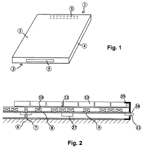
Figure 1 shows a possible embodiment of the proposed modular illuminating tile
shown
by way of example only. Illuminating tile 1 is realised as a thin plate with a
substan-
tially rectangular, in the present case square area, similar to a floor tile
or wall tile; in
the figure, its upper side 2 and bottom side 3 are plane, and its lateral edge
4 along the
perimeter lies in planes which are perpendicular to sides 2 and 3,
respectively. In the
example shown here, the surface of lateral edge 4 is plane, with only male
connector 5
forming the connecting means extending at the respective opposite ends of
illuminating
tile 1, of which one is represented by a dotted line only.
Figure 2 is the schematic representation of the cross section of the structure
of illumi-
nating tile 1 shown in Figure 1. Illuminating tile 1 ¨ of which one piece is
shown in its
entirety, but only parts of the adjacent illuminating tiles 1 are shown on the
left and
CA 02844341 2014-01-10
WO 2013/008145 PCT/1B2012/053414
- 7 -
right sides ¨ is fixed on substrate 6 through an intermediary adhesive layer
7. Carrier
board 8 is fixed to the adhesive layer 7 by gluing and in the example shown
here, it is a
double-sided printed circuit board comprising in the figure at its bottom side
a wiring 9
made by any known process, e.g. by etching, for the purpose of the
transmission of elec-
trical energy, and on its upper side illuminating elements 10 serving for the
illumination
of illuminating tile 1 are fixed. In the present example, illuminating
elements 10 are
light-emitting diodes (LEDs) emitting light of a colour which may be freely
chosen,
which are fixed on the carrier board 8 by e.g. SMD technique. On each of the
two, left
and right, sides of the illuminating tile 1 presented here, connection means
11 are
formed, the preferential and potential realisation of which will be shown in
more detail
later on. A further adhesive layer 12, in present case a transparent one, is
applied on the
carrier board 8 in a way covering also the illuminating elements 10, which
protects,
among other things, the layers, elements and units under it, hence carrier
board 8 and il-
luminating elements 10, against any mechanical and weather effects, while also
provid-
ing an appropriate base for gluing mosaic pieces 13 letting the light through
to a prede-
fined extent onto it.
The basic unit of the wall cover composed of single modular illuminating tiles
accord-
ing to the invention is the module shown in Figure 2. It may be of any size,
starting
from a single mosaic piece 13, it may be of a size corresponding to a
plurality of mosaic
pieces 13. Thanks to the connection system being applied, the modules of
illuminating
tile 1 constituting a wall cover can be connected to each other in diverse
ways, and these
structures, of the shape of a string, a star or any other form, are connected
to the outside
world via one or several interfaces to be presented later on. Thus the
majority of illumi-
nating tiles 1 can be accessed via another illuminating tile 1; this has the
advantage that
anyone can produce an individual active surface from predefined illuminating
tiles 1.
The function of the external adhesive layer 12 is to protect the electronic
components
and units located in the layers underneath from the environmental impacts, so
the mate-
rials to be used for this purpose must be chosen so as to be highly resistant
to tempera-
ture, humidity and UV radiation; this choice can be securely performed by an
expert or
a person skilled in the art based on his relevant knowledge. If necessary,
adhesive layer
12 can also be waterproof. To the adhesive layer 12 is connected a cover layer
made of
external decorative mosaic pieces 13 which are fixed onto the individual
illuminating
CA 02844341 2014-01-10
WO 2013/008145 PCT/1B2012/053414
- 8 -
tiles 1 prior to or after their installation.
Illuminating tile 1 is meant to illuminate, that is, to generate light; to
transmit the exter-
nal effects, forces impacting on mosaic pieces 13 to substrate 6. Illuminating
tile 1
comprises the electronic parts, of which Figure 2 illustrates the light-
emitting diodes
constituting light units 10 and the printed circuit board constituting carrier
board 8. The
upper adhesive layer 12 of illuminating tile 1 is a homogenous, translucent,
water-tight,
hard adhesive layer 12. It embraces the electronic parts and provides for the
homoge-
nous distribution of heat on the surface. The function of adhesive layer 7
applied as bot-
tom layer is to fix illuminating tile 1; in the present case, it is a cement-
based material,
so its properties correspond to those of cover materials used by construction
industry.
The simplest type of modular illuminating tile 1 according to the invention
comprises il-
luminating elements 10 and connecting means 11, supported and fixed by a
carrier
board 8. In upgraded embodiments, illuminating tile 1 is controlled from the
exterior; so
it comprises a control unit not shown in the figure, and in some embodiments
also an in-
telligent control system in a loop-through array on an internal data bus in
the known
way, and the control unit on the one hand and its regulators and interfaces on
the other
hand are connected to this internal data bus.
In a further, upgraded embodiment of the proposed illuminating tile 1, the
internal
communication bus system is complemented by a bus designed to transmit control
sig-
nals corresponding to the various illuminating picture segments from the
control unit to
the appropriate areas.
Illuminating tiles 1 belonging to the same module family can be joined
universally, by
any of their connecting means 11. Connecting means 11 are equivalent, that is,
there is
no dedicated output or input connecting means, hence the individual
illuminating tiles 1
can connect freely, from any direction. Optional accessories, not shown and
mentioned
to keep this presentation simple, but well-known to those skilled in art, such
as negative
edge, positive edge etc. provide for creative integration.
Through the appropriate design of connecting means 11 and carrier boards 8,
illuminat-
ing tiles 1 can also be fastened together in a flexible way, in which case the
individual
modules will be sufficiently flexible at the module boundaries for the active
surface
composed of illuminating tiles 1 to adhere to any 3D surface provided that the
modules
CA 02844341 2014-01-10
WO 2013/008145 PCT/1B2012/053414
- 9 -
are sufficiently small, as e.g. in the case of an illuminating tile 1 made of
mosaic pieces
13.
Illuminating tile 1 may be surrounded, as the case may be, by a mounting frame
35 the
width of which corresponds to the aggregate height of carrier board 8,
illuminating ele-
ment 10 and the protective cover.
In yet another upgraded embodiment of the proposed illuminating tile 1, an
energy stor-
ing element 37 is fixed on carrier board 8, which may be, as will be known to
those
skilled in the art, a battery, a condenser storing the energy feeding
illuminating tile 1, or
even a solar unit in optical connection with the external surface of carrier
board 8. En-
ergy storage unit 37 may be linked to connecting means 11 through diodes not
illus-
trated separately, connected also in the known way in blocking direction.
Figures 3a-3c show a possible embodiment of connecting means 11 in more
detail. As
can be seen, connecting means 11 comprises connector sleeves 14, soldered in
the
printed circuit board constituting the carrier board 8 by their lead-out wire
15, and their
distal end extend beyond the carrier board 8. Connector sleeves 14 integrated
into the
individual illuminating tiles 1 ¨ positioned, as appropriate, in illuminating
tiles 1 joined
together modularly exactly opposite one another ¨ are designed so as to be
able to re-
ceive one connector pin 16 each, which provide permanent and good electrical
connec-
tion due to the adequate choice of the material of connector sleeve 14 and
connector pin
16, e.g. due to silvering. In the case under study, a shoulder 17 is created
on the middle
of connector pin 16, preferably made of some insulating material, e.g.
plastic, the func-
tion of which is, on the one hand, to prevent that connector pin 16 should
sink too
deeply into connector sleeve 14 and, on the other, for two illuminating tiles
1 placed
closely side by side, this shoulder 17 closes the inputs of the connector
sleeves 14, as
can be seen in Figures 3b and 3c. Due to the materials used and the soldering
technique,
this design permits also an angle divergence of a certain degree between the
individual
illuminating tiles 1; the position/angle ever of the illuminating tiles 1
placed in their fi-
nal position is then fixed definitively by adhesive layer 7 and adhesive layer
12.
The electricity input and, as the case may be, the electric control signals
are transmitted
from one illuminating tile 1 to another by connecting means 11 between the
illuminat-
ing tiles 1. Connecting means 11 are good electrical conductors. Preferably
the connec-
CA 02844341 2014-01-10
WO 2013/008145 PCT/1B2012/053414
- 10 -
tion points are airtight to avoid potential corrosion problems; this is
ensured on both
sides in the manner presented here by the adhesives used for adhesive layer 7
and adhe-
sive layer 12, respectively.
It is conceivable that in special cases it is more advantageous to apply
inductive cou-
pling, of a lower efficiency, instead of plug-in power supply, e.g. for mobile
systems or
systems which can be configured in alterably manner. For this purpose, we
exploit the
known effect that at high frequencies magnetic field can carry the necessary
electric
power between two illuminating tiles 1 through an air gap 18 between them. A U-
shaped iron core 19 is placed in the peripheral zone of each illuminating tile
1, with a
coil 20 arranged on it. In the adjoined illuminating tiles 1, magnetic field
will be closed
through the iron core 19 parts separated merely by air gap 18 and a minimum
adhesive
layer 7, which ensures that energy supplied by coil 20 of one illuminating
tile 1 should
induce sufficient voltage in the adjacent coil 20 of the neighbour
illuminating tile 1.
Figure 4 is a schematic representation of this possible embodiment.
If power supply is provided locally, but control and the connection between
the individ-
ual illuminating tiles 1 can only be established without wiring, e.g. to
provide for com-
munication between the interactive mosaic surfaces of elevators and a control
panel, an
other wireless connection can also be applied, which may be realised by radio
frequency
units such as the radio modules of the German Hoperf company, or the Bluetooth
or
Zigbie connection well-known in information technology. All three
communication in-
terfaces offer modules which can be connected to control unit 22 via a serial
port. If
need be, the system can be connected to remote controllers, mobile
applications or to a
smart phone. RFID allows many creative solutions, such as user identification,
custom-
tailored colours/animation, entry/information system built into the cover
panels, or in a
hotel the owner of a card drawn at the end of the corridor can be guided home
by ani-
mation/an arrow moving on the floor etc.
Figure 8 shows how to maintain connection between individual illuminating
tiles 1 in a
safe way also in case of unexpected breakdown. This is ensured by redundant
control
and supply, a solution that is self-repairing and error-resistant to some
extent, the extent
being determined by the level of redundancy being applied. To prevent contact
errors
due to corrosion, dilatation movements, and to provide for alternative
solutions in case
CA 02844341 2014-01-10
WO 2013/008145 PCT/1B2012/053414
- 11 -
of malfunction, the number of connectors applied in connecting means 11 can be
multi-
plied and hence connector redundancy can be created. The distribution of the
connectors
is of the 1:N type redundant distribution, that is, the same signal or voltage
is transmit-
ted through several connecting pegs.
Pixel redundancy is applied to provide protection against the malfunction or
obsoles-
cence of illuminating elements 10 applied in illuminating tiles 1. The life-
span of light-
emitting diodes can only be estimated, so 1:N redundancy is provided through
the alter-
native control of reserve light-emitting diodes for breakdown cases; the life-
span of the
individual illuminating tiles 1 can thus be raised n-fold.
Control and power supply to systems and sub-systems within the individual
illuminating
tiles 1 is provided from several directions to prevent any illuminating tile 1
errors
caused by a point-like defect.
As can be seen in Figure 8, adaptive redundant control, that is, bi-
directional control and
power supply can be applied in case of the failure of the cover illumination
such as
damage to the cover, corrosion, parts failure etc. In such cases, the system
presented
here can recognise errors of a certain level and identify an alternative route
for the nec-
essary control and power supply. Where the energy supply chain is broken, this
is de-
tected by a control unit designed in a way which is suitable for that purpose,
and supply
is launched also from the other end-point. A similar process is followed for
the data
traffic: if no feedback signal is received, control signals are being sent
with the help of
an appropriate control unit from both directions.
Figure 5 presents the electrical structure of an illuminating tile 1 at block
diagram level.
In this embodiment shown by way of example only, connecting means 11 are
mounted
at both ends of illuminating tile 1 which are electrically connected to one
another and to
a power supply 21. Power supply 21 ensures the power supply of the electrical
parts in
the illuminating tile 1 in the known way; for the sake of simplicity, the
conductors con-
cerned are omitted from the figure. Illuminating tile 1 comprises a control
unit 22, a mi-
crocontroller to be presented in more detail later, one input of which is
connected to
connecting means 11, and one output to the other connecting means 11. In the
case pre-
sented here, the three control outputs of control unit 22 are connected to the
control in-
puts of one semiconductor switching element FET1, FET2, FET3 each, and the
outputs
CA 02844341 2014-01-10
WO 2013/008145 PCT/1B2012/053414
- 12 -
of the semiconductor switching elements FET1, FET2, FET3 are connected via a
series
resistor R to one output respectively of light-emitting diodes 23 arranged in
groups of
three. The other output of light-emitting diodes 23 is connected to the output
of a driver
stage 24 each; the driver stages 24 are connected in series to one another,
and the input
of the first driver stage 24 connects to a further output of control unit 24,
and the output
of the last control unit 24 connects to a further input of control unit 22.
Control unit 22
comprises a clock generator, the output of which is led to respective further
inputs of
each driver stage 24.
The illuminating tile 1 shown in the figure is a module of the size of 5x12
mosaics, pro-
viding for an RGB or monochrome static redundancy level of max. n=3, without
intelli-
gent error repair, but each pixel is illuminated by several light-emitting
diodes 23. As it
can be seen in the figure, illuminating tile 1 comprises three areas the light
intensities of
which can be set from the outside independent of each other.
At the start, control unit 22 expects the signal from both directions, that
is, from both
connecting means 11, and when it receives it through a connecting means 11
acting as
input from either side, it defines its other port as an output, and transmits
data through
that. Its task is to control the three semiconductor switching elements FET1,
FET2,
FET3 regulating the light intensity of the field of the three light-emitting
diodes 23
through the modification of the filling factors. In the case presented here a
high-
frequency control is applied for physiological reasons, lest it should disturb
the envi-
ronment. Supply unit 21 comprises polarity and overcurrent protection, in the
exem-
plary way shown in Figure 6, and it also comprises a DC-DC transducer 24 which
con-
verts an input voltage, higher in the present case, down to the appropriate
voltage level.
The individual light-emitting diodes 23 are operated with the help of R
resistors adjust-
ing the appropriate operating points.
Figure 6 illustrates a possible embodiment of polarity and overcurrent
protection in
power supply 21. From electronic point of view, this provides for polarity-
independent
connection allocation and protection. Four diodes D1 to D4 in the figure are
in Graetz
connection, and they connect to inputs Inl and In2 of power supply 21, whereas
to the
output of the Graetz rectifier bridge on the one hand an suppressor diode SD
is con-
nected in the normal way and, on the other, it is connected through a fuse B1
to the out-
CA 02844341 2014-01-10
WO 2013/008145 PCT/1B2012/053414
- 13 -
puts Out+ and Out¨ of power supply 21. If a voltage spike appears in the
supply voltage
under the inductive effect of a nearby lightning, for example, the suppressor
diode SD
will not let this spike through towards the electronic parts of illuminating
tile 1, but will
heat them away, distributed between the diode bridge consisting of diodes D1
to D4 and
the conductor resistance. Four-diode rectification makes the input polarity-
independent.
If the system breaks down, fuse B1 switches off power supply 21 and the
electronic
units of illuminating tile 1 from the supply input, but when the error is
repaired, e.g. the
overload is terminated, it switches it back.
Figure 7 depicts a wiring diagram of another possible embodiment of the power
supply
21. In addition to the connection presented in Figure 6, power supply 21
comprises a
DC-DC transducer 24 realised in the given case by an integrated power circuit
of type
LM2596S, the connection and operation of which can be traced in power circuit
cata-
logues. One output of the full-wave rectifier bridge made up of the diodes D1
to D4 is
connected to the input VIN of DC-DC transformer 24, whereas the other output
of the
bridge is tied to ground GND. The direct current input VCC of power supply 21
con-
nects to the same input, and a filter capacitor Cl is connected in between the
input VIN
of DC-DC transducer 24 and its joined inputs ON/OFF and GNDIN, the latter
being
also connected to ground GND. The cathode of a Schottky diode D5 and one
output of
smoothing reactor Ll are connected to the output OUT of DC-DC transducer 24.
The
anode of the Schottky diode D5, together with the other output of filter
capacitor C2
connecting to the other output of the smoothing reactor Ll and the output TAB
of DC-
DC transducer 24 are connected to ground GND. A voltage divider consisting of
resis-
tors R1 and R2 and parallel with the resistor R1 a filter capacitor C3 are
connected to
the output of smoothing reactor Ll, and the joint point of the voltage divider
is led back
to input FB of the DC-DC transducer 24. The output of smoothing reactor Ll
consti-
tutes at the same time also the output of the power supply 21, onto which a
load RL is
connected. The voltage of the system and the operating point of light-emitting
diodes 23
can be set by adjusting resistors R1 and R2.
Figure 9 is the schematic representation of a possible embodiment of
connecting means
11 and its wiring diagram. As can be seen, in the presented embodiment, one
connecting
means 11 is a 20-pin connector, where 5-5 connector pins 16 and connector
sleeves 14,
respectively, provide for the transmission of the positive and negative supply
voltage
CA 02844341 2014-01-10
WO 2013/008145 PCT/1B2012/053414
- 14 -
IN+, IN-, while 2-2 connector pins 16 and connector sleeves 14, respectively,
provide
for the redundant transmission of the mosi and miso control signals,
respectively.
Figure 10 shows connection details of relevance for the microcontroller of the
type AT-
INY13-8SC constituting the control unit 22. The input GND of controller device
22 is
connected to ground; its input VCC is connected to the supply voltage, and a
filter ca-
pacitor C4 is inserted between them. Outlets Fl, F2 and F3 of control unit 22
are led to
the control electrodes of semiconductor switching elements FET1, FET2, FET3
outlined
in Figure 5; two of these, namely semiconductor switching elements FET2 and
FET3,
and light-emitting diodes 23 and resistors R associated with them are also
represented
here. As can be seen, output F2 of the control unit 22 is tied to the control
electrode of
the field effect transistor constituting semiconductor switching element FET2
through a
resistor R3 which is connected also to the ground GND through a resistor R4,
whereas
the source electrode of the semiconductor switching element FET2 is connected
to
ground GND and its drain electrode connects through a resistor R to the
cathode of
light-emitting diodes 23, and the anode of light-emitting diodes 23 are
connected jointly
to the driver stage 24.
If the system comprising the proposed illuminating tiles 1 breaks down and it
is not re-
stored even after restart, it may be necessary to replace an illuminating tile
1. This is a
rather cumbersome task, since the cover has to be undone and then remade
without
leaving any external marks. The first step for that is to dismount the mosaic
cover: cut
along the module boundary with due precision e.g. by a diamond cutting disc
which is
thinner than the joint. As a second step, lift out the defective illuminating
tile 1, and
clean the cavity so created so as to be able to place a replacement
illuminating tile 1 into
it. As a third step, try to place the replacement module into the emptied
cavity, to be
sure you managed to create sufficient space, and then replace the impervious
layer by
administering a commercially available impervious layer. Wait until it dries
and then
put illuminating tile 1 into the bed formed by adhesive layer 7 and check its
correct op-
eration. As a fourth step, after drying, close the cover by using cover
materials which
are identical with the original ones.
Figure 11 outlines a novel illuminating tile 26 suitable for repairing or,
more precisely,
replacing such a defective illuminating tile 1. As can be seen, the carrier
board 8 of the
CA 02844341 2014-01-10
WO 2013/008145 PCT/1B2012/053414
- 15 -
illuminating tile 26 is not a single printed circuit board, but consists of
four carrier
board slices 28 to 31, connected to each other in the plane of the carrier
board 8 sup-
porting the illuminating elements 10 by hinge points 27, and the carrier board
slices 28
to 31 are connected to one another by some known flexible sealing agent 32.
There are
connecting means 11 on the carrier board slices 28 and 31, formed and fixed in
the way
disclosed above. Thanks to the design presented here, the illuminating tile 26
is com-
pressible and its relevant size is smaller in compressed state than the size
of the previous
defective illuminating tile 1 dismounted, probably by destruction, and in this
state it can
be inserted in between two other illuminating tiles 1 fixed already originally
onto the
substrate 6, and thanks to the flexible sealing agent 32 it will regain its
original form
and size once installed, and its connecting means 11 will enter into
electrical connection
with the appropriate connecting means 11 of the two adjacent non-defective
illuminat-
ing tiles 1. The installed illuminating repair tile 26 must be put in an
appropriate adhe-
sive layer 7, and after placement the external adhesive layer 12 and mosaic
pieces 13
must be restored so as to protect it from mechanical damage and from any
detrimental
environmental effect and, as the case may be, to ensure also its water-
resistance this
way.
Figure 12 shows a possible embodiment of the printed circuit board
constituting the car-
rier board 8 of the illuminating tile 1, with conductors 25 providing the
wiring of the il-
luminating tile 1, and Figure 13 shows the other side of the printed circuit
board which
already comprises light-emitting diodes 23 constituting the illuminating
elements 10,
semiconductor switching elements FET1, FET2, FET3 and the microcontroller
consti-
tuting the control unit 22. Of course, the position and number of the
individual compo-
nents, the shape and size of carrier board 8 depend on the illuminating tile 1
ever and
they can be configured freely.
Figure 14 shows a schematic view of a possible embodiment of an illuminating
tile 1
comprising, in addition to the components listed already, a further
communicator and
sensor unit 33, which can sense, for example, the change in temperature, in
the incom-
ing light intensity, the proximity of an object T, etc. To that effect, as the
case may be, a
sensor opening 34 must be left between mosaic pieces 13, if the communicator
and sen-
sor unit 33 has optoreflective or -capacitive properties, albeit infra beams
can pass
through mosaic pieces 13. The output of communicator and sensor unit 33 may,
for ex-
CA 02844341 2014-01-10
WO 2013/008145 PCT/1B2012/053414
- 16 -
ample, be connected to the appropriate control input of the control unit 22 in
the illumi-
nating tile 1, depending on the type of the microcontroller ever constituting
the control
unit 22. Control device 22 can be programmed, for example, so as to change
colour
based on information from the temperature sensor integrated in the
illuminating tile 1 in
the whole or in part of the illuminating tile 1, or to display animation,
change light in-
tensity etc.
It is possible to detect by the optoreflective or -capacitive method the
touching of cer-
tain areas of the surface of the illuminating tile 1. By way of example, in
line with the
mosaic pattern, highly creative things can be made with its help, for example,
by mak-
ing the icons of the control keys out of mosaic pieces and by providing them
with touch
sensors or, for example, through connection with the water works system, it is
possible
to select the water strength and temperature by touching the mosaic of a
washbasin/shower cabin. The essence of optoreflective operation is the
presence of infra
light, i.e. light of a spectrum which is invisible to the naked eye, besides
the coloured
light-emitting diodes 23. When one touches the surface, this light is
reflected, and that is
detected in known way by an infra sensor. Lest other infra sources should
disturb the
system, the infra signal is modulated, and the sensor detects only the
modulated, re-
flected, infra signal.
Generally, light transmittance by the cover or in particular of mosaic pieces
13 consti-
tuting it is constant in both directions. Thus it is not only possible to emit
light, but also
to measure the ambient light. It is possible to draw inferences as to the time
of the day
from the relative value of light intensity. This is what happens e.g. in case
of light inten-
sity depending on ambient light: at night, the cover must hardly emit any
light, whereas
at noon higher light intensity is needed to produce the same effect,
Furthermore, for
physiological reasons, preferably warmer light temperatures are used in the
evening,
which promote relaxing, whereas at daytime cooler illuminating improving the
capacity
for concentration is more expedient. To compensate for the decline in light
output of
light-emitting diodes 23 during their life-time, aging, the programme of
control unit 22
can be designed so that light-emitting diodes 23 be provided an input of
increasing
power which has a compensatory effect resulting in higher light emission, in a
simpler
case on the basis of the well-known signal curves or, for more precise
results, by apply-
ing special light measurement, of course within the limits of the threshold
values of the
CA 02844341 2014-01-10
WO 2013/008145 PCT/1B2012/053414
- 17 -
devices concerned. Extra heat generated in the meanwhile can be borne by
illuminating
tile 1 without suffering any damage.
Every illuminating tile 1 receives surface filling, which is not only
advantageous in case
of a possible malfunction, but also distributes the temperature over the
carrier board 8.
The adhesion capacity of the layer poured onto it is enhanced by pins mounted,
in the
simplest case soldered, in a scattered way on the printed circuit board
constituting the
carrier board 8, not shown in the figures, similarly to concrete armouring.
Connecting
means 11 are soldered on the side of the printed circuit board opposite light-
emitting di-
odes 23, so as to make perfect light generation possible at the connection
points. The
height of the parts is below light beam of light-emitting diodes 23 and filter
capacitors
Cl to C3 are recessed through windows cut in the printed circuit board.
The parts are installed in function of the order ever, since each product can
have differ-
ent numbers of light-emitting diodes 23. Separate installation files are made
for the
manufacturing robots for each product regarding the illumination of different
forma-
tions, coloured pictures, including the colour and installation position of a
given light-
emitting diode 23, the intensity of the colour concerned regulated by
resistors R located
next to light-emitting diodes 23.
The program operating the proposed modular illuminating tiles, if any, is most
simple.
At start, a control unit 22 monitors both of its communication outputs. When
it receives
data from one direction, it defines the other communication array as output
and trans-
mits data of two types: pixel information and command. For pixel information,
the data
channel functions similarly to a shift register: when the control unit
receives new data, it
forwards the package stored previously. When each storage unit has its own
pixel data,
a command runs along the chain which is forwarded promptly upon interpretation
by
every tile 1 it then displays the new light intensities/colours.
The individual illuminating tiles 1 can be combined as easily as LEGO pieces
so as to
satisfy the changing demands.
Once the program code is burnt into the control unit 22, it is cast with the
help of a
mould, so that illuminating tile 1 should obtain its final form. Its top is
covered by trans-
lucent epoxy-based mosaic adhesive, and in a second stage its bottom is
covered by ce-
ment-based adhesive. These two impermeable layers protect the internal
electronic parts
CA 02844341 2014-01-10
WO 2013/008145 PCT/1B2012/053414
- 18 -
from mechanical effects and shorts and corrosion caused by water. The cement-
based
rear/under plane is important for adhesion/adherence, and the resin-based
front plane is
compatible with the majority of adhesives used to stick up translucent covers.
The finished illuminating tiles 1 are always subjected to testing and the
measured pa-
rameters are evaluated. The parameters being measured may include power drain,
tem-
perature, behaviour at maximum voltage, concussion, water-resistance etc.
The illuminating tile 1 is characterised by properties similar to common tile
coverings.
It is made of materials used by construction industry (e.g. cement-based
adhesives),
which promotes easy installation. When installed, illuminating tiles 1 are
step-proof,
since they transmit any force impacting on the surface to the base; they have
water-
proof coating, and even a water-tight layer may be put around them after
installation.
This double layer prevents any shorts and corrosion. Light does no damage to
illuminat-
ing tiles 1. The UV effect of the Sun may be detrimental, since with time it
erodes the
surface of the materials and reduces their light transmission capacity or
temperature in-
crease at high temperatures may activate the protective circle of some
illuminating tiles
1 and the modules may switch off. But high temperature due to protracted
exposition to
sunlight may be detrimental even in shut-down state. Owing to their known
features,
light-emitting diodes are sensitive to high temperature which increases the
number of
micro-fissures in the semi-conducting material which, in turn, reduces
efficiency.
The materials applied in illuminating tile 1 are identical to the cover
materials used
most frequently by construction industry, and hence their heat expansion
properties are
also similar. Consequently, the entire surface moves together, preventing the
generation
of any tension, crack, defect.
The light transmission capacity of the applied internal materials diminishes
with time
under the effect of UV light, and fissures due to wear and dilatation also
reduce the light
transmission capacity.
Weight and surface of an illuminating tile 1 are near-identical with that of
the common
floor tile coverings. Consequently, the stability factor of their fixing by
gluing is also
similar. Glass mosaics represent a preferred covering in airplanes and vessels
due to
their smaller volume. On demand, they can also be manufactured with a rear
plane cast
in foam, which makes the construction even lighter.
CA 02844341 2014-01-10
WO 2013/008145 PCT/1B2012/053414
- 19 -
Since the surface is covered by a common covering, every property is
determined by
that circumstance. The wear of the surface depends on the quality of the
covering layer.
List of reference signs:
1 tile B1 fuse
2 side Out+, Out¨ output
3side 24 DC-DC transducer
4 edge VIN input
5 male connector VCC input
6 substrate ON/OFF input
7 adhesive layer GNDIN input
8 carrier board GND ground
9 wiring Cl, C2, C3, C4 filter capacitor
10 illuminating element OUT output
11 male connector D5 Schottky diode
12 adhesive layer Ll smoothing reactor
13 mosaic piece Tab output
14 connector sleeve R, R1, R2, R3 resistor
15 lead-out wire FB input
16 connector pin mosi, miso control signal
17 shoulder Fl, F2, F3 output
18 air gap 25 conductor
19 iron core 26 tile
20 coil 27 articulated joint
21 power supply 28-31 carrier board slice
22 control unit 32 sealing agent
FET1, FET2, FET3 semiconductor 33 communicator and sensor unit
switching element 34 sensor opening
23 light emitting diode (LED) 35 mounting frame
24 driver stage 36 opening
D1 to D4 diode 37 energy storing element
Inl, In2 input T object
SD suppressor diode RL load