Note: Descriptions are shown in the official language in which they were submitted.
CA 02845113 2014-02-12
WO 2013/030787 PCT/1B2012/054471
IMPLANTS WITH WEAR RESISTANT COATINGS AND METHODS
FIELD OF THE INVENTION
[0001] The present invention relates to wear resistant implants, and in
particular implants
including a wear resistant coating. The present invention also relates to
methods of producing
such implants.
BACKGROUND OF THE INVENTION
[0002] Joint replacement is one of the most commonly performed orthopaedic
operations.
A total joint replacement has an average life span of about 15 years. The
reason for implant
failure may be due to one or more of several factors, but often is caused by
wear particles from
the bearing surface of the implant. Wear particles from implants have been
linked to
inflammation which lead to bone loss and, eventually, implant loosening,
Sargeant et al, "Hip
Implants: Paper V. Physiological Effects", Materials & Design, 27 (2006) 287-
307. The
chemistry and particle size of such particles have been found to be of high
importance to the
inflammation response, Sargeant et al (2006) and Sargeant et al, "Hip Implants
- Paper VI - Ion
Concentrations", Materials & Design 28 (2007) 155-171.
[0003] Cobalt chromium (CoCr) based metals are commonly used as biomaterial
for
implants and have been shown to be relatively good, biocompatible materials
for joint
applications. Their mechanical properties are adequate for use as load-bearing
joint implants.
However, experiments have shown that CoCr particles released from implants due
to wear and
corrosion can restrain bone growth, Aspenberg et al, "Benign response to
particles of diamond
and SiC: bone chamber studies of new joint replacement coating materials in
rabbits",
Biomaterials, 17 (1996) 807-812. Titanium alloys and stainless steels have
also been used
frequently in joint implants, Sargeant et al (2006). The main risks with metal
alloy implants are
1
CA 02845113 2014-02-12
WO 2013/030787 PCT/1B2012/054471
release of metal ions due to corrosion and wear, and these metal ions can be
carcinogenic. The
wear particles may also lead to bone resorption, Sargeant et al (2007).
[0004] Use of a liner of ultra high molecular weight polyethylene (UHMWPE)
against a
metal or ceramic head, having a relatively low measured coefficient of
friction, has been
proposed, but the UHMWPE liner often gets worn and produces a relatively large
amount of
wear particles that can cause aseptic loosening, Xiong et al, "Friction and
wear properties of
UHMWPE/A1203 ceramic under different lubricating conditions", Wear, 250 (2001)
242-245.
[0005] Alumina (A1203) and zirconia (Zr02) ceramics have been used in joint
replacements to provide high wear resistance and chemical inertness. However,
ceramic
materials have a poor tensile strength and alumina components in joint
replacements have been
shown to release wear particles due to low toughness. The particles released
from alumina and
zirconia are also inert and will not be resorbed by the body. However, there
are other ceramic
materials that have shown promising results. For example, silicon nitride
(Si3N4) has a higher
fracture toughness and is more resistant to microcrack propagation than
alumina, Bal et al,
"Fabrication and Testing of Silicon Nitride Bearings in Total Hip
Arthroplasty: Winner of the
2007 'HAP PAUL Award", The Journal of Arthroplasty, 24 (2009) 110-116.
[0006] One solution to the problems related to bulk metal joint implants or
ceramic joint
implants is to coat a metal joint with a more wear resistant, low corrosion
ceramic coating, for
example, a titanium nitride coating. However, the problems of inert wear
particles causing long
term problems such as inflammation and aseptic loosening have not been
resolved.
[0007] Accordingly, a need exists for wear and corrosion resistant
biomedical implants,
especially for use as artificial joints, to overcome the problems of wear
particle formation and
assorted high inflammation.
2
CA 02845113 2014-02-12
WO 2013/030787 PCT/1B2012/054471
SUMMARY OF THE INVENTION
[0008] Accordingly, it is an object of the invention to provide implants
and methods
which overcome various disadvantages of the prior art.
[0009] In one embodiment, the invention is directed to an implant
comprising a substrate
and a coating on a surface of the substrate, the coating comprising silicon
nitride and having a
thickness of from about 1 to about 15 micrometer.
[0010] In another embodiment, the invention is directed to a method of
providing an
implant which comprises coating a surface of an implant substrate with a
coating comprising
silicon nitride and having a thickness of from about 1 to about 15 micrometer
by physical vapour
deposition.
[0011] The implants and methods of the invention are advantageous in
providing implants
with a combination of properties suitable for use in vivo while also
exhibiting improved wear
resistance and, particularly, reduced tendency to release wear particles
causing inflammation and
implant loosening. Particularly, particles released by the present implants
are resorbable and
reduce the possibility of inflammation and implant loosening resulting from
wear particles.
[0012] These and additional advantages, objects and embodiments of the
invention will be
more fully apparent in view of the following detailed description.
BRIEF DESCRIPTION OF THE DRAWINGS
[0013] The detailed description will be more fully understood in view of
the drawings, in
which:
[0014] Fig. 1 shows X-ray diffraction (XRD) patterns of Si,Ny-coatings on
CoCr
substrates and of CoCr substrates, as described in Example 1.
[0015] Figs. 2A and 2B show transmission electron microscopy (TEM) images
of coating
No. 8, as described in Example 1: Fig. 2A shows selected area electron
diffraction (SAED),
3
CA 02845113 2014-02-12
WO 2013/030787 PCT/1B2012/054471
which corresponds to Si3N4; Fig. 2B shows a high resolution TEM (HRTEM) image
of an Si3N4
lattice within the coating.
[0016] Figs. 3A and 3B show the surface appearance of coatings at two
magnifications,
using scanning electron microscopy (SEM), 67 sample tilt, as described in
Example 1: Fig. 3A
is Coating no. 5 on Si-substrate; Fig. 3B is Coating no. 2 on CoCr substrate.
[0017] Figs. 4A-4D show SEM images of cross sections of coatings on silicon
wafer
showing the resulting coating micro structure, as described in Example 1: Fig
4A shows Coating
no. 3 with a fine columnar structure; Fig 4B shows Coating no. 5 with a
columnar structure; Fig
4C shows Coating no. 8 with a columnar structure; Fig 4D shows Coating no. 10
without a
distinct columnar structure.
[0018] Fig. 5 shows the coefficient of friction versus number of
revolutions for Si,Ny-
coatings, bulk CoCr and bulk Si3N4, as described in Example 1. The gray area
represents the
region in which almost all the coating curves are within, except coating no. 2
and 5 (not shown in
the graph).
[0019] Fig. 6 is an SEM image of surface appearance of the wear-tracks on
coating no. 8
after 10,000 revolutions at two different magnifications, 67 sample tilt, as
described in Example
1. The coating is smoothed out in the wear-track.
[0020] Fig. 7 shows optical profile images of worn surfaces and the
calculated cross-
sectional areas of the wear-tracks. The z-scale is magnified 23 times more
than the x,y-scale.
[0021] Figs. 8A-8C show the different structures (a) dense, (b) laminar and
(c) columnar
materials, respectively, as described in Example 2.
[0022] Fig. 9 shows scratches on coatings deposited on silicon wafers for:
Panel a) Si,Ny-
coating No. 16, b) Si,Ny-coating No. 12, c) SixIslyCz-coating No. 20 deposited
with a Si-target
4
CA 02845113 2014-02-12
WO 2013/030787 PCT/1B2012/054471
power of 4 kW, and d) Si,NyC,coating No. 22 deposited at 1 kW, as described in
Example 2.
The arrow indicates the direction of scratching.
[0023] Fig. 10 shows friction coefficient versus number of revolutions from
Ball-on-Disc
test for tests run for 10,000 cycles, as described in Example 2.
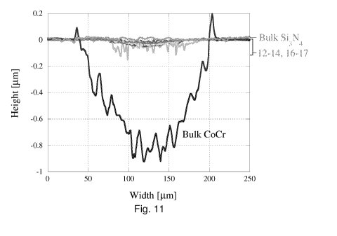
[0024] Fig. 11 shows the cross-section of the wear tracks after 10,000
revolutions in ball-
on-disc test, as described in Example 2.
[0025] Figs. 12A and 12 B show XRD spectra of a) Si,Ny- and b) Si,NyCz-
coatings,
respectively, as described in Example 2.
[0026] Figs. 13A-13D show SEM images of coating 12 with additional
treatment steps, as
described in Example 2: an increased adhesion from Fig. 13A, wherein the
standard process has
been obtained, to Fig. 13 B, introducing an etch process prior deposition,
Fig. 13 C, with
intermittent bias steps, and Fig. 13D, with a nitrogen gradient and high
frequency during
deposition.
[0027] Fig. 14 shows Coating 12 with a thickness of 8 pm, as described in
Example 2.
[0028] Fig. 15 show the concentration of free Si in PBS solutions of
different pH after 35
and 75 days, as described in Example 2.
[0029] Fig. 16 shows the concentration of silicon in PBS, measured with
inductively
coupled plasma atomic emission spectroscopy (ICP-AES) , as described in
Example 2.
[0030] The Drawings are non-limiting of the invention defined in the
claims.
DETAILED DESCRIPTION
[0031] The present invention relates to implants comprising a substrate and
a coating.
The coating is wear resistant with high mechanical strength and forms
resorbable wear particles.
The invention also relates to methods of providing wear resistant biomedical
implants.
CA 02845113 2014-02-12
WO 2013/030787 PCT/1B2012/054471
[0032] The implant substrate may be any desired implant material. In
specific
embodiments, the substrate may be ceramic or metallic. Suitable metals can be
found in the
group of cobalt-chromium alloys, stainless steel alloys, titanium and titanium
alloys. In antoher
embodiment, the substrate may be formed of ultra high molecular weight
polyethylene
(UHMWPE). Combinations of two or more of these materials may also be employed.
In a more
specific embodiment, the substrate is a Cobalt-Chromium alloy. The substrate
may be cleaned
and/or polished to a very fine surface finish prior to coating. In one
embodiment, the substrate is
polished to provide a surface finish of below (Ra) 10 nm in surface roughness
prior to receiving
the wear resistant coating according to the present invention, as a rough
substrate typically
increases the generation of wear particles as compared with a smooth surface
and, conversely, a
smooth surface will reduce the tendency to generate wear particles. Within the
present
disclosure, surface roughness is measured with an optical profiler in PSI
(phase-shifting
interferometry) mode over an area of ¨400 x 500 pm, using a x10 lens and FOV 1
in a Wyko,
NT-110 Veeco, as described by Kim, "Surface Roughness of Ceramic Femoral Heads
after In-
Vivo Transfer of Metal Correlation to Polyethylene Wear", Bioceramics and
Alternative
Bearings in Joint Arthroplasty, J.-D. Chang, K. Billau (Eds.), Steinkopff
(Pub.), 2007, pp. 49-57.
[0033] The coating material is based on silicon nitride and the coating has
a thickness of
from about 1 to about 15 micrometer. In a specific embodiment, the coating has
a thickness of
from about 1 to about 10 micrometer. Above about 15 micrometer, the coating
adhesion is too
weak, while below about 1 micrometer, the coating life time is too short. As
discussed in further
detail below, the coating is formed using a physical vapour deposition (PVD)
method. In
specific embodiments, the hardness of the coating ranges between 5- 45 GPa,
or, more
specifically, from about 15 to 45 GPa, measured with a commercial nanoindenter
(CSM
6
CA 02845113 2014-02-12
WO 2013/030787 PCT/1B2012/054471
Instruments UNHT) with a Berkovich tip, using the Oliver-Pharr method (Oliver
et al, An
improved technique for determining hardness and elastic modulus using load and
displacement
sensing indentation experiments, Journal of Materials Research, 7 (1992) 1564-
1583).
Measurement of elastic modulus is also made using the Oliver-Pharr method.
[0034] In specific embodiments, the coating as deposited has a surface
roughness of less
than about 50 nm, more specifically less than about 20 nm. In further specific
embodiments, the
coating can be polished to a fine surface roughness below about 10 nm in
roughness, using
methods known in the art. In additional specific embodiments, the coatings
have a coefficient of
friction less than about 0.5, more specifically, less than about 0.3, or, more
specifically, less than
about 0.25. In further embodiments, the coating has a wear resistance after
10,000 revolutions in
bovine serum solution of less than about 10 x 10-7 mm3/Nm, measured according
to the
technique as described in Example 1.
[0035] The coating can be single layered, multilayered and/or of
compositional gradient
structure, and may optionally be provided with an adhesion layer if desired.
The coating may be
crystalline, nanocrystalline or amorphous, or a combination of crystalline,
nanocrystalline and
amorphous. The coating can also comprise crystals embedded into an amorphous
phase. In
specific embodiments, the coating comprises Si3N4 , or is of the formula
SixIsly, where 2<x<4 and
3<y<5, and may be either of a-phase, 11-phase, gamma phase or amorphous phase,
or
combinations thereof. A typical average grain size in the coating is below 1
micrometer, or more
specifically, below 500 nm, to provide a high strength coating. In more
specific embodiments,
the average grain size is larger then about 1 nm.
[0036] The coating may also comprise additions of C, H, 0 or combinations
thereof. In
specific embodiments, the substitutions are individually below 20 atomic %,
and, in a more
7
CA 02845113 2014-02-12
WO 2013/030787 PCT/1B2012/054471
specific embodiment, are combined less than 20 atomic %. Thus, in specific
embodiments, the
silicon nitride coating has a composition of SixIslyWz, where W is C, H and/or
0, and 2<x<4 and
3<y<5 and z is such that the material contains less than 20 atomic percent of
C, H and O. For
very high degrees of substitution the lattice structure is not stable and
other less wear resistant or
non-resorbable phases will form.
[0037] When wear particles are released from the coating, the wear
particles are small, in
certain embodiments, below 1 micrometer, and in further embodiments, below 100
nanometer.
Such particles hence have a large surface area compared to their volume, which
increases the
dissolution rate for the particles in body fluid.
[0038] The coating as described is preferably formed by PVD, and in a
specific
embodiment, is deposited using reactive sputtering, where nitrogen gas (N2) is
let in to the
chamber and reacts with the sputtered molecules (here, predominately Si) from
a target (a
silicon-containing material). Suitable flow rates of N2 and argon (Ar) are
shown in Table 1. Also,
other gases can be provided to the chamber for reaction with the sputtered
atoms. For example,
ethylene, C2H4, which results in a coating containing carbon and hydrogen, can
be provided to
the chamber. A preferred flow rate of C2H4, if employed, is shown in Table 1.
The target is
suitably silicon. Additional exemplary targets include, but are not limited
to, silicon carbide and
silicon nitride. The power of the target is suitably from 150 W and higher. In
specific
embodiments, the sputtering process is performed using radio frequency
sputtering, for example,
with a frequency of above 10 kHz, more specifically, 13.56 kHz.
[0039] In a more specific embodiment, the coatings according to the present
invention are
deposited using high-power pulsed magnetron sputtering (HiPIMS). The coatings
can then be
deposited using a silicon target in a Ar/N2 atmosphere. Extra carbon may
optionally be obtained
8
CA 02845113 2014-02-12
WO 2013/030787 PCT/1B2012/054471
in the coatings using a carbon target, or from a gas/liquid containing carbon,
for example, C2H4.
The samples can be rotated in the chamber to obtain depositions of both the
silicon and the
carbon target. Deposition parameters, such as target power and temperature in
the chamber, may
be varied to form different microstructures and compositions, as demonstrated
in the Examples.
See Table 3. Suitable parameters for additional embodiments of the deposition
of the coatings
are also indicated in Table 4.
[0040] The substrate temperature during the coating process may be varied
as desired. In
specific embodiments, the temperature is from about 100 C to 600 C, more
specifically, from
about 200 to 400 C. The chamber pressure during the coating process may be
varied as desired.
In specific embodiments, the chamber pressure is normally from about 0.510-6
to 2-10-5 bar. In
specific embodiments, the working gas is normally argon gas.
[0041] The aforementioned additives (C, H, 0) and/or the deposition process
may be may
be used to control the hardness, elastic modulus, wear resistance, solubility,
surface energy
and/or chemical affinity, for example, the retention of synovial fluid on the
coating surface in
vivo, of the coating. Thus, the additives and/or the deposition process can
influence the
functionality of the coating. A higher solubility of the coating provides a
faster resorption of
wear particles when formed in vivo. The solubility is, in one embodiment,
controlled via solid-
state substitutions in the silicon nitride lattice. Generally, for SixIsliy
coatings, a higher hardness
and a higher elastic modulus are obtained when the coating is applied with
lower Si-target
power, for example, in the range of 1 kW to 4 kW. Generally, for SixIsliyCz
coatings, a lower
surface roughness is obtained when the coating is applied with lower Si-target
power, for
example, in the range of 1 kW to 4 kW. Additionally, the composition may be
vaied to obtain a
desired crystalline structure. For example, dense microstructures having a
higher wear resistance
9
CA 02845113 2014-02-12
WO 2013/030787 PCT/1B2012/054471
may be obtained with SixIsliy coatings, while columnar and laminar structures
may be obtained
with Sixl\liyC, coatings.
[0042] The implants may be of any desired physical form for use in various
body
locations, and a portion or the entirety of the substrate may be coated with
the coating according
to the invention. For joint implants, the head or the cup can be coated but it
is preferable that
both components are coated with the silicon nitride-based coating. Both
components can have
the same type of substrate, e.g. cobalt chromium ¨ cobalt chromium, or may be
of different
materials. Also, in modular hip joints, both the male and female parts may be
coated to reduce
the wear. For knee joint implants, either just the femoral or the tibial
component, or both
components, are coated with the silicon nitride-based coating as described
herein. For elbow
joint implants, either just the bearing parts of the ulnar component, the
humeral component, the
bearing and the hinge pin, or all of these parts can be coated. Also,
components for other joints,
including, but not limited to, the shoulder, wrist, angle, fingers and toes,
orthopaedic and dental
screws, needles and plates, can be provided with the silicon nitride-based
coating as described
herein.
[0043] Examples
[0044] The following Examples demonstrate various embodiments of the
invention,
providing silicon nitride coatings on CoCr substrates, and testing various
properties of the
implants.
[0045] Example 1
[0046] SixIsly-coatings were deposited on CoCr substrates of type ASTM
F1537 and also
on silicon wafer substrates. First, the substrates were polished to a surface
roughness (Ra) of
about 8 nm. Prior to deposition, the substrates were ultrasonically cleaned in
acetone and ethanol
CA 02845113 2014-02-12
WO 2013/030787 PCT/1B2012/054471
for 5 min each. The coatings were deposited using reactive RF sputtering
(13.56 kHz) utilising a
silicon target with Ar/N2 plasma atmosphere. Several process parameters were
varied in order to
optimise the coating composition and microstructure, see Table 1. For two of
the coatings
ethylene (C2H4) gas was introduced into the chamber as a reactive agent in
order to dope the
coatings with C. All substrates were heated during deposition, except for
coating No. 2. To avoid
overheating of the target, the coating process alternated between 10 min
sputtering, and a 3 min
break, for a total sputtering duration of 2 hours, except coating No. 3 which
had a coating
duration of 3 hours. The parameters for coating No. 1 were the start
parameters and the
parameters for the other coatings were varied from that combination.
Table 1. Parameters during coating processes.
Coating Substrate Ar N2 Pressure T ( C) C2H4 Target
No. (sccm) (sccm) (Pa) (partial Power
pressure, (W)
Pa)
1 CoCr 10 30 1.0 280 0 300
2 Si CoCr 10 30 1.0 25 0
300
3 Si CoCr 10 30 1.0 280 0
150
4 Si CoCr 10 30 0.5 280 0
300
Si CoCr 10 30 1.5 280 0 300
6 CoCr 30 15 1.0 280 0 300
7 CoCr 20 20 1.0 280 0 300
8 Si CoCr 20 20 1.5 280 0
300
9 Si - 20 20 0.5 280 0 300
Si CoCr 10 30 1.3 280 9-104 300
11 Si CoCr 10 30 1.3
280 1.5-104 300
[0047] The coatings were evaluated with nano-hardness measurements. It was
revealed
that the coating hardness was approximately 22 GPa, which is about the same as
for bulk Si3N4.
[0048] Coating analysis
[0049] EDS
(Energy Dispersive Spectroscopy) analysis revealed that the coatings
contained about 3-5% C, 54-60% N and 36-41% Si, based on atomic %, and the
individual
composition for each coating can be seen in Table 2. It should be noted that
there is a general
11
CA 02845113 2014-02-12
WO 2013/030787 PCT/1B2012/054471
error when determining compositions using EDS of about 2 atomic %, this
should be added to
limits above.
[0050] No crystalline structure in the coatings was detected in x-ray
diffraction (XRD),
see Fig. 1. The only observed crystalline reflections could be indexed to Co,
Cr and Co3Mo,
using International Centre for Diffraction Data, Reference files: Cobalt PDF
no. 15-0806,
Chromium PDF no. 88-2323, and Cobalt Molybdenum PDF no. 29-0488. But a
distinguished
amorphous bump in the diffraction from the coating (especially for No. 8) at
20-35 , was
observed, see Fig. 1.
[0051] Selected area electron diffraction (SAED) of coating No. 8 using
transmission
electron microscopy (TEM) produced ring-like patterns with sharp dark
speckles, representing a
nanocrystalline structure, Figure 2A. Via indexing the electron diffraction
pattern, it was evident
that all rings represented Si3N4. Furthermore, high resolution TEM (HRTEM)
images exhibit
lattice fringes consistent with a polycrystalline material, Figure 2B. This
means that the coatings
are nanocrystalline and amorphous.
[0052] Almost all the SixIsly-coatings exhibited a fine surface
nanostructure, as
exemplified in, Fig. 3A. The only exception was coating No. 2 (deposited with
a lower substrate
temperature) which showed thin coating patches, Fig. 3B. The surface roughness
(Ra) of coating
No. 2 is too high, about 250 nm, while for the other coatings it is about 5 nm
on Si substrates and
nm on CoCr substrates. This corresponds to a Ra of about 3 and 8 nm for the Si
and CoCr
substrates, respectively, prior to the coating deposition.
[0053] The images of cross sections of the coatings show that the character
of the coating
structure differs, as shown in Figs. 4A-4D. Coatings Nos. 5 and 8 (Figs. 4B
and 4C) have a
columnar structure and a thickness of approximately 1.4 um. Coating No. 3,
Fig. 4A (lower
12
CA 02845113 2014-02-12
WO 2013/030787 PCT/1B2012/054471
power supplied to target) has a similar structure to coatings Nos. 5 and 8,
but with finer columns
and the coating thickness is just approximately 600 nm. Coating No. 10, Fig.
4D (deposited with
C2H4), is approximately 1.2 lam thick, has a much coarser microstructure than
coatings Nos. 3, 5
and 8, but not as distinct columnar structure. Each coating, except coating
No. 3 had a thickness
of 1.2-1.8 lam, however that variation could be within one sample as well, due
to the decreasing
deposition rate from the centre below the target.
[0054] Friction and wear test
[0055] The coatings were tribologically tested using a ball-on-disc
apparatus, where the
coated discs were slid against a stationary polished ball of Si3N4 (6 mm in
diameter, Spekuma,
Sweden, representing a coated counter surface) while the coefficient of
friction was continuously
measured. The procedure was conducted in a similar manner as ASTM F 732-00
(Standard Test
Method for Wear Testing of Polymeric Materials Used in Total Joint Prostheses,
ASTM
International, 2006). Under the ball, the tested material was rotated, forming
a wear track of 5
mm in diameter at a speed of 0.04 m/s and normal load 1 N at room temperature.
The wear test
was run in a serum solution of 25% fetal bovine serum (Gibco) with sodium
azide and ethylene-
diaminetetraacetic acid (EDTA) according to ASTM F 732-00. The wear rate is
quantified with a
specific wear rate according to
Specific wear rate = Wear volume . (Eq 1)
Load-Sliding Distance
[0056] The wear rate, excluding the ball, was calculated from the worn
cross-sectional
area, measured with vertical scanning interferometry (VSI, Wyko NT-110). The
friction
measurements revealed no distinct difference in coefficient of friction
between the different
types of coatings, and bulk CoCr, Fig. 5. The major part of the coatings had a
coefficient of
13
CA 02845113 2014-02-12
WO 2013/030787 PCT/1B2012/054471
friction between 0.12 and 0.22, indicated by the grey area in Figs. 4A-4D.
Almost all tests started
with relatively fast and short friction decrease and then a longer increase of
the coefficient of
friction to then stabilise after about 2000 revolutions. However, coating No.
2 (deposited with a
lower substrate temperature) had a coefficient of friction at 0.3, much higher
than the rest of the
coatings.
[0057] The low wear rate of the coating demonstrates the potential of these
coatings for
use on bearing surfaces of joints. The coating topography was gradually
smoothed out during
sliding against the Si3N4-ball, in bovine serum solution, like coating No. 8,
Fig. 6.
[0058] The specific wear rate of the coatings after 10,000 revolutions was
about 3 x 10⁻⁷
mm3/Nm, Fig. 7. In this image, where the z-scale has a higher magnification,
grooves along the
wear-track are visible in the coating wear-track as well. The wear amount of
the coatings was
similar to bulk Si3N4 which had a specific wear rate about 1 x 10⁻⁷ mm3/Nm.
For CoCr, the
specific wear rate was much higher, about 60 x 10-7 mm3/Nm.
[0059] Hardness
[0060] Hardness of the coatings was obtained with a commercial nanoindenter
(CSM
Instruments UNHT) with a Berkovich tip. A total of 30 indents per smaple were
completed with
a maximum depth of 50 nm. Hardness and elastic modulus were determined with
the Oliver-
Pharr method.
[0061] Summary of the coating properties
[0062] Despite the variation of several deposition parameters, not much
difference in the
chemical composition, phase composition, nanostructure, tribological
properties or hardness, see
Table 2.
Table 2. Coating properties as well as atomic composition for some of the
tested coatings.
Atomic ratio (%)
14
CA 02845113 2014-02-12
WO 2013/030787 PCT/1B2012/054471
Coating la C Si N Specific wear Mean hardness (GPa)
(coefficient rate
of friction (mm3/Nm)
1 0.15 5 40 54 3.0 = 10-7 21.5 2.7
2** 0.3 4 36 60 * 24.2 3.0
3 0.2 4 41 55 2.7 = 10-7 21.2 2.0
4 0.15 4 40 56 3.2 = 10-7 22.3 2.5
8 0.15 3 39 58 3.2 = 10-7 18.0 2.2
0.15 5 39 56 3.0 = 10-7 21.6 3.7
* The coating roughness was higher than the wear scar
** The coating was deposited at lower temperature
[0063] Example 2
[0064] Si,Ny- and Si,NyCz-coatings were deposited on silicon wafers (001)
with high-
power pulsed magnetron sputtering system (HiPIMS, CemeCon CC800/9, Germany).
The
vacuum chamber (85x85x100 cm) of the industrial-scaled deposition system is
equipped with
four rectangular magnetron sputtering cathodes (50x8.8 cm) facing a table
holder in the center.
Unipolar pulses were applied to the magnetrons by a pulsing unit (SINEX 3,
Chemfilt
Ionsputtering AB, Sweden) charged by a direct current (DC) power supply
(Pinnacle, Advanced
Energy). The depositions were made with a silicon target with Ar/N2
atmosphere. A Si-target
(purity 99.999%) was used for all depositions. Extra carbon is obtained on a
number of coatings
(Nos. 18 to 28) with a carbon target (purity 99.5%). The samples are then
rotated in the chamber
to get depositions of both the silicon and the carbon target at a distance of
7.5 cm from the
targets. For SiN coatings, the substrate was static perpendicular to the Si-
target, and for SiCN
coatings, the substrates where rotated. Deposition parameters, such as target
power and
temperature in the chamber, were varied to form different microstructures and
compositions, see
Table 3. The constant parameters during deposition can be seen in Table 4.
Substrates were
cleaned ultrasonically in acetone and ethanol, in 5 min sequences, and dried
in dry N2 gas before
being introduced into the chamber.
CA 02845113 2014-02-12
WO 2013/030787
PCT/1B2012/054471
Table 3. Deposition parameters for SixNy- and SixNyCz-coatings on silicon
wafers.
(*) are also deposited in CoCr-substrate (ASTM F75).
Coating
Si-target C-target Temperature
Coating thickness
Power [W] Power [W] [ C]
[1-tml
12 1000 0 250 1.2
13 2000 0 250 2.8
14 3000 0 250 4.3
15 4000 0 250 4.4
16 2000 0 520 2.5
17 3000 0 520 3.8
18* 4000 500 250 0.50
19* 4000 700 250 0.50
20 4000 1400 250 0.55
21 1000 700 250 0.40
22 1000 1000 250 0.85
23 1000 1400 250 0.80
24* 4000 500 520 1.10
25 4000 700 520 0.70
26 4000 1400 520 0.70
27 1000 700 520 0.70
28 1000 1000 520 0.70
Table. 4. Parameters held constant for all depositions.
Pressure [Pa] 0.4
Ar flow [sccm] 360
N2 flow [sccm] 60
Bias [V] -100
Pulse freq [hz] 300
Pulse width [is] 200
Substrate Si-wafer
[0065] The
surface roughness (Ra) of the coatings on Si-wafer substrates are around 10
nm, for samples deposited in CoCr-substrates the Ra's are around 20 nm when
measured over an
area around 0.3 mm2. When measured over 1 pm2 the surface roughness of the
coating on Si-
wafers was from 0.3 to 4 nm.
16
CA 02845113 2014-02-12
WO 2013/030787 PCT/1B2012/054471
[0066] The coatings showed three different types of structure seen in cross-
section, dense
(coatings Nos. 12-17), laminar (coatings Nos. 18-20 and 24-26) and columnar
(coatings Nos. 21-
23 and 27-28), see Figs. 8A-8C.
[0067] Hardness measurements were performed as in Example 1, but at a
maximum depth
of 40 nm. The elastic modulus is determined from these measurements with
Poisson's ratios of
0.25 for coatings and the reference material Si3N4 (Walmsley et al, Poisson's
Ratio of Low-
Temperature PECVD Silicon Nitride Thin Films, Journal of
Microelectromechanical Systems,
16 (2007) 622-627), and 0.3 for CoCr were assumed.
[0068] The hardness for SixIslyCz-coatings ranges from 9 to 19 GPa and
SixIsly-coatings
from 17 to 21 GPa. The elastic modulus of the SixIslyCz-coatings was from 167
to 212 GPa and
SixIsly-coatings ranges from 148 to 218 GPa, see Table 6.
[0069] The adhesion and cohesion has been investigated with micro
scratching, see Fig. 9.
The cohesive failure types for SixIslyCz-coatings, cracks and flakes, are
believed to be related to
different microstructures for coatings deposited at different Si-target
powers. When deposited on
CoCr, the failure loads was only half of that on Si-wafers. This was expected,
due to the softer
substrate material and the poor adhesion to CoCr.
[0070] Friction and wear test
[0071] Wear and friction tests were preformed in the same manner with a
Ball-on-Disc
test as in Example 1. The SixIsly-coatings tested for 10,000 revolutions has a
friction coefficient
around 0.20-0.28 (excluding coating No. 15), see Fig. 10. SixIslyCz-coatings
did not show the
same wear resistance and worn through the coating before 1000 revolutions.
[0072] The worn cross-sections are displayed in Fig. 11. The calculated
specific wear rate
is given in Table 6.
17
CA 02845113 2014-02-12
WO 2013/030787 PCT/1B2012/054471
[0073] Composition
[0074] XRD shows no crystalline structure in the coating, only small
amorphous bumps
could be seen, Fig. 12.
[0075] EDS analysis showed the compositions in the coatings, see Table 5.
The C content
ranges from 0 to 2 at.% without use of the carbon target, and 6 to 35 at.%
with the carbon target.
The Si was from 37 to 77 at.% and N was from 19 to 29. Note, as above, that
the general error
when determining compositions using EDS is about 2 at.%. XPS analysis
confirms that the
silicon atoms bond to nitrogen atoms.
[0076] Summary of the coating properties
[0077] The coating properties and composition of Example 2 are summarized
in Table 5
and 6. The SixNy-coatings showed similar wear resistance as in Example 1 as
well as a slightly
lower hardness.
Table 5. Atomic composition for some of the coatings. Values marked with (*)
are tested on CoCr-
substrate.
Coating Atomic ratio (%)
C Si N
12 1 69 29
13 2 74 24
14 1 75 23
15 0 76 22
16 1 74 23
17 1 77 21
18 6 68 25
18* 8 68 23
19 9 65 25
19* 9 66 23
20 14 62 22
21 23 46 26
22 30 40 26
23 35 37 24
24 6 70 24
24* 8 70 22
25 9 71 19
26 15 66 18
27 22 49 26
28 29 44 25
18
CA 02845113 2014-02-12
WO 2013/030787 PCT/1B2012/054471
Table 6. Mechanical properties of some coatings. Values marked with (*) are
tested on CoCr-
substrate.
Coating Stable Specific Mean hardness Mean elastic
Cohesive Adhesive failure SD
Il wear rate SD modulus SD failure SD (mN)
(mm3/Nm) (GPa) (GPa) (mN)
12 0.21 1.3 = 10-7 21.2 3.1 212
18- 214 12
13 0.24 2.2 = 10-7 18.4 2.1 212
14- 260 15
14 0.28 2.3 = 10-7 17.2 3.1 199
22- no rupture
15 >0.33 240 = 10-7 17.2 3.0 199
30- no rupture
16 0.20 2.1 = 10-7 18.8 2.6 201
12- 265 8
17 0.27 4.8 = 10-7 18.8 1.1 167 8-
no rupture
18 - 16.0 1.6 199 15 68 6 85 5
18*- IVa 16.3 2.8 216 25 26 2 36 5
19- - 15.2 1.7 196 12
55 2 81 7
19*- IVa 16.1 2.3 202 16 20 3 33 4
20- - 14.8 3.5 178 27
65 7 83 8
21- - 10.7 1.4 148 12
39 6 46 3
22- - 11.1 1.6 149 12
42 2 52 8
23- - 9.9 1.6 137 13
36 2 42 1
24- - 18.5 1.6 210 10
68 6 80 4
24*- IVa 17.0 3.9 218 33 35 3 67 5
25- - 18.2 1.6 216 11
77 3 95 5
26- - 18.6 2.5 202 17
68 5 86 2
27- - 17.5 2.1 218
16 86 9 105 15
28- - 15.4 2.6 195 18
62 4 76 2
Sl3N4 1.0 = 10-7 7.4 0.7 210 14 IVa IVa
CoCr 60 = 10-7 24.5 4.5 314 26 IVa IVa
[0078] Increased adhesion
[0079] The coatings from Example 2 have been further developed to increase
the
adhesion with an etch process before the deposition as well as with
intermittent bias steps or with
a nitrogen gradient and high frequency during the deposition. The processes
are described in
Tables 7 and 8. The difference in adhesion is shown in Fig. 13 in a Rockwell
test with a load of
100 kg.
[0080] Other
alternatives on improving the adhesion may be made by adhesion layers
such as Si or Cr, or a pulsed table as well as targets. Intermittent bias
steps and gradients are used
to decrease residual stresses and improve the adhesion of the coating.
Table 7. Etch process for an increase in adhesion.
19
CA 02845113 2014-02-12
WO 2013/030787 PCT/1B2012/054471
Power Ti-target [W] 1500
Ar flow [sccm] 353
Kr flow [sccm] 267
Etch Bias [V] -200
Temperature [ C] ¨325
Duration [s] 180
Table 8. Coating processes for increased adhesion.
Process Standard Bias steps Gradient nitrogen and high
frequency
Si-target power [kW] 1 1 1
Pressure [Pa] 0.4 0.4 0.4
Ar flow [sccm] 360 360 360
N2 flow [sccm] 60 60 0 to 100,
in steps of 1 sccm/ 60 s, then 60
Bias [V] -100 5x(-100 for 1400 s, -500 for 200 s) -
100
Pulse freq [hz] 300 300 500
Pulse width [is] 200 200 200
Temperature [ C] ¨325 ¨325 ¨325
[0081] High thickness
[0082] Coatings with high thickness around 10 to 15 pm can be obtained. An
example of a
thick version of coating 12 is shown in Fig. 14.
[0083] Solubility test
[0084] Due
to the very low amount of wear particle formation in the tests, it is very
difficult
to measure the dissolution rate of the actual wear particles using the methods
known to the
inventors. Instead, a commercial silicon nitride powder (P95H, Akzo Nobel) was
mixed with
PBS using three different pH values: 4.8, 6.5 and 7.4. PBS has a natural pH of
7.4 and
hydrochloric acid was added to decrease the value. The mixture was stored in
plastic tubes with
plastic lids. The tubes were placed on a rocking platform shaker and stored at
37 C during 35
and 75 days respectively (Table 9). The average grain size of the powder was
approximately 1
um (measured with SEM and optical microscopy). 100 mg of silicon nitride
powder was mixed
with 15 ml PBS. After the storage time, the mixture was filtered through a 0.2
um PTFE
CA 02845113 2014-02-12
WO 2013/030787 PCT/1B2012/054471
membrane using a syringe. Subsequently to the filtration, ICP-MS (Inductively
Coupled Plasma
Mass Spectrometry) was used to determine the silicon ion content of the
solutions.
Table 9. Solubility test: number of samples per pH and time point.
100 mg Si3N4-powder PBS without powder
pH 4.8 6.5 7.4 4.8 6.5 7.4
Time (days)
35 4 4 4 1 1 1
75 4 4 4 1 1 1
[0085] The concentration of free Si in the filtered solutions indicates
that some of the powder
has been dissolved. The concentration of Si in the filtered PBS solutions was
about 75 m1/1 for all
pH variations and also approximately the same for the different incubation
periods, see Fig. 15.
All samples of PBS solutions without any addition of powder showed Si
concentrations of less
than 0.5 m1/1.
[0086] Amorphous silicon nitride particles (approx. 30-50 nm) were
investigated for
exhibiting dissolution also in phosphate buffered saline (PBS, pH -7.3, 37 C),
Fig. 16. The
particles are separated from the PBS by centrifugation.
[0087] The tests showed that wear resistant, low friction silicon nitride
coatings can be
produced at deposition temperatures above about 100 C. The wear resistance
was considerably
higher than that of CoCr alone and similar to bulk silicon nitride ceramics.
In addition, silicon
nitride particles were shown to dissolve in simulated body fluids.
[0088] The results show that it is feasible to deposit silicon nitride
films using sputtering
techniques and that the films are more wear resistant than the substrate
material. In addition
silicon nitride is slowly dissolved in simulated body fluids.
[0089] The specific examples and embodiments described herein are exemplary
only in
nature and are not intended to be limiting of the invention defined by the
claims. Further
21
CA 02845113 2014-02-12
WO 2013/030787 PCT/1B2012/054471
embodiments and examples, and advantages thereof, will be apparent to one of
ordinary skill in
the art in view of this specification and are within the scope of the claimed
invention.
[0090] References
[1] A. Sargeant and T. Goswami, Hip implants: Paper V. Physiological effects,
Materials &
Design 27 (2006) 287-307.
[2] A. Sargeant and T. Goswami, Hip implants - Paper VI - Ion concentrations,
Materials &
Design 28 (2007) 155-171.
[3] P. Aspenberg, A. Anttila, Y.T. Konttinen, R. Lappalainen, S.B. Goodman, L.
Nordsletten,
and S. Santavirta, Benign response to particles of diamond and SiC: bone
chamber studies of
new joint replacement coating materials in rabbits, Biomaterials 17 (1996) 807-
812.
[4] D. Xiong and S. Ge, Friction and wear properties of UHMWPE/A1203 ceramic
under
different lubricating conditions, Wear 250 (2001) 242-245.
[5] B.S. Bal, A. Khandkar, R. Lakshminarayanan, I. Clarke, A.A. Hoffman, and
M.N. Rahaman,
Fabrication and Testing of Silicon Nitride Bearings in Total Hip Arthroplasty:
Winner of the
2007 "HAP" PAUL Award, The Journal of Arthroplasty 24 (2009) 110-116.
[6] R.R. Wang, G.E. Welsch, and O. Monteiro, Silicon nitride coating on
titanium to enable
titanium¨ceramic bonding, Journal of Biomedical Materials Research 46 (1999)
262-270.
[7] M. Matsuoka, S. Isotani, W. Sucasaire, L.S. Zambom, and K. Ogata, Chemical
bonding and
composition of silicon nitride films prepared by inductively coupled plasma
chemical vapor
deposition, Surface and Coatings Technology 204 (2010) 2923-2927.
[8] S.-L. Ku and C.-C. Lee, Surface characterization and properties of silicon
nitride films
prepared by ion-assisted deposition, Surface and Coatings Technology 204
(2010) 3234-3237.
22
CA 02845113 2014-02-12
WO 2013/030787 PCT/1B2012/054471
[9] H.P. Lobl and M. Huppertz, Thermal stability of nonstoichiometric silicon
nitride films made
by reactive dc magnetron sputter deposition, Thin Solid Films 317 (1998) 153-
156.
[10] K. Kazuo and N. Shinji, Ceramic-coated prosthetic implants, in Japan
Kokai Tokyo Koho,
N.S.P. Co, Editor. 1989: Japan.
[11] L. Huang, K.W. Hipps, J.T. Dickinson, U. Mazur, and X.D. Wang, Structure
and
composition studies for silicon nitride thin films deposited by single ion
bean sputter deposition,
Thin Solid Films 299 (1997) 104-109.
[12] International Centre for Diffraction Data, Reference files: Cobalt PDF
no. 15-0806.
[13] International Centre for Diffraction Data, Reference files: Chromium PDF
no. 88-2323.
[14] International Centre for Diffraction Data, Reference files: Cobalt
Molybdenum PDF no. 29-
0488.
23