Note: Descriptions are shown in the official language in which they were submitted.
CA 02847649 2016-03-10
CA 2,847,649 Replacement Page RED-001-CA-DIV3
METHOD AND SYSTEM FOR REDUCING A TIME SKEW BETWEEN TWO
POLARITIES OF A DIFFERENTIAL SIGNAL
The present invention is a divisional of Canadian Patent Application No.
2,628,017, filed January
17, 2007.
RELATED APPLICATIONS
The present patent application claims priority from the US provisional patent
application Ser. No.
60/759,985 to Judith REA et al. entitled "AN IMPROVED DATA RECOVERY SYSTEM FOR
SOURCE SYNCHRONOUS DATA CHANNELS" filed on January 19, 2006.
FIELD OF THE INVENTION
The present invention relates to data recovery systems, and in particular, to
an improved data
recovery system for source synchronous data channels.
BACKGROUND OF THE INVENTION
The distribution of television signals has increasingly become based on
digital methods and digitally
encoded forms of video and audio signals. At the same time, higher resolution
(high definition TV)
has become available in the market place, commensurate with larger and higher
definition displays.
To meet the requirement of interconnecting such high definition displays with
digital signal sources
such as Digital Versatile Disc (DVD) players and receivers/decoders for
digital satellite and digital
cable distribution of video material, a digital interface standard has
evolved, known as the
High-Definition Multimedia Interface (HDMI). A detailed specification for HDMI
can be obtained
from the "hdmi.org" website. The HDMI specification currently available and
used in this
application is HDMI specification version 1.2 dated August 22, 2005. This HDMI
standard can be
employed for connecting digital video sources to digital video sinks over a
cable that carries a
number of digital signals and a clock signal.
This interface, being capable of running at a very high data rate presents a
number of challenges that
need to be solved, in order that cost-effective hardware implementations can
be manufactured for
1
CA 02847649 2014-08-27
CA 2,847,649 Replacement Page RED-001-CA-DIV3
the consumer market.
Existing technologies commonly used in high performance telecommunications
equipment could be
employed to build HDMI receivers and transmitters, but would scarcely meet the
cost, power, and
size targets implied by the consumer market.
Consequently there is a need for the development of innovative techniques to
enable a data recovery
system for a low-cost, low-power HDMI receiver.
SUMMARY OF THE INVENTION
There is an object of the invention to provide an improved data recovery
system for a HDMI
receiver.
According to one aspect of the invention, there is provided a system for
reducing a time skew
between two polarities of a differential signal representing a digital bit
stream, comprising:
(a) a variable delay for inserting a variable time delay into polarities of
the differential signal
for generating a deskewed signal;
(b) a multi-phase clock for generating a number M of clock phases per bit of
the digital bit
stream for oversampling the deskewed signal into a digital representation of
the deskewed signal;
(c) a logic circuit for estimating the quality of the digital representation
of the deskewed
signal; and
(d) a means for adjusting the variable delay in response to the estimated
quality of the digital
representation of the deskewed signal to improve said quality.
In the system described above, the variable delay is configured to insert a
variable time delay into
one or the other polarity of the differential signal.
In the system described above, the variable delay is a variable analog delay.
2
CA 02847649 2014-08-27
CA 2,847,649 Replacement Page RED-001-CA-DIV3
In the system described above, the variable analog delay comprises:
a number of analog delay units arranged sequentially;
a means for selecting a composite delay resulting from selected analog delay
units; and
a means for inserting the composite delay into polarities of the differential
signal to reduce
the time skew.
The system of any one described above further comprises an equalizer circuit
for adjusting a
frequency response of the deskewed signal to produce an equalized signal.
The system described above further comprises a phase compensator for aligning
a phase of the
equalized signal and a phase of a clock signal.
In the system described above, the phase compensator comprises:
an analog phase detector generating an analog delay control signal; and
a programmable analog delay circuit in a path of the differential signal for
changing the
phase of the equalized signal in response to the analog delay control signal.
In the system described above, M equals to one of the following:
M=3;
M=12;
M = 3 to 12.
In the system described above, the variable analog delay comprises one or more
amplifiers.
In the system described above, the differential signal is a High Definition
Multimedia Interface
(HDMI) signal.
According to another aspect of the invention, there is provided a method for
reducing a time skew
between two polarities of a differential signal representing a digital bit
stream, comprising the steps
of:
3
CA 02847649 2014-08-27
CA 2,847,649 Replacement Page RED-001-CA-DIV3
(a) generating a deskewed signal by inserting a variable delay into polarities
of the
differential signal;
(b) generating a multi-phase clock signal having at least M phases per bit of
the digital bit
stream;
(c) oversampling the deskewed signal with the multi-phase clock into a digital
representation
of the deskewed signal;
(d) estimating the quality of the digital representation of the deskewed
signal; and
(e) adjusting the variable delay in response to the estimated quality of the
digital
representation of the deskewed signal to improve said quality.
In the method described above, the step (a) comprises inserting the variable
delay into one or the
other polarity of the differential signal.
In the method described above, the step (a) comprises inserting a variable
analog delay.
In the method described above, the inserting the variable analog delay
comprises:
arranging a number of analog delay units sequentially;
selecting a composite delay resulting from selected analog delay units; and
inserting the composite delay into polarities of the differential signal to
reduce the time skew.
The method described above further comprises adjusting a frequency response of
the deskewed
signal to produce an equalized signal.
The method described above further comprises aligning a phase of the equalized
signal and a phase
of a clock signal.
In the method described above, the alignin further comprises:
generating an analog delay control signal; and
changing the phase of the equalized signal in response to the analog delay
control signal.
4
CA 02847649 2014-08-27
CA 2,847,649 Replacement Page RED-001-CA-DIV3
In the method described above, M equals to one of the following:
M=3;
M=12;
M = 3 to 12.
In the method described above, the inserting comprises inserting the variable
analog delay having
one or more amplifiers.
In the method described above, the differential signal is a High Definition
Multimedia Interface
(HDMI) signal.
Thus, a method of deskewing a differential signal, and a system and circuit
therefor have been
provided.
BRIEF DESCRIPTION OF THE DRAWINGS
An embodiment of the invention will now be described, by way of example, with
reference to the
accompanying drawings in which:
Figure 1 shows a block diagram of a HDMI receive interface 100 of the
embodiment of the
invention;
Figure 2 shows an overview of the Data Recovery Slice 132 of the HDMI receive
interface 100 of
Fig. 1;
Figures 3a and 3b show timing diagrams of the single ended signal components
and the
corresponding differential signal of the differential data on a HDMI channel
respectively as they
might be transmitted by an HDMI transmitter;
Figures 4a and 4b show example timing diagrams of the single ended signal
components and the
corresponding differential signal of the differential data as they might be
received by an HDMI
5
CA 02847649 2014-08-27
CA 2,847,649 Replacement Page RED-001-CA-DIV3
receiver from the cable;
Figure 5 a simplified block diagram of the Differential Deskew block 204 of
the Data Recovery
Slice 132 of Fig. 2;
Figure 6 shows the preferred embodiment of the adjustable delay block 300 of
the Differential
Deskew block 204 of Fig. 5;
Figure 7 shows a simple RC delay circuit;
Figure 8 shows simulation results of the RC circuit of Fig. 7;
Figure 9 shows simulation results of the RC circuit of Fig. 7, but with a
reduced time constant;
Figure 10 shows a delay circuit made from a cascade of RC stages;
Figure 11 shows simulation results of the circuit of Fig. 10;
Figure 12 shows a cascaded delay circuit with buffers;
Figure 13 shows simulation results of the circuit of Fig. 12;
Figure 14 shows a simple follower circuit;
Figure 15 shows an AC-coupled follower circuit;
Figure 16 shows a simplified block diagram of a buffered delay stage 400 as an
implementation of
the delay unit 306 of the adjustable delay 300 of Fig. 6;
Figure 17 shows an implementation of the buffer 404 of the buffered delay
stage 400 of Fig. 16;
6
CA 02847649 2014-08-27
CA 2,847,649 Replacement Page RED-001-CA-DIV3
Figure 18 shows a simple N-channel follower;
Figure 19 shows a modified buffer 404B as an alternative implementation of the
buffer stage for the
delay stage 306 of Fig. 6;
Figure 20 shows typical waveforms at the input and the output of a cable;
Figure 21 shows a simplified transfer function of a cable;
Figure 22 shows an equalized transfer function;
Figure 23 shows a block diagram of an exemplary implementation 500 of the
Linear Phase
Compensator 210 of Fig. 2;
Figure 24 shows a diagram illustrating data phase shifting in the Programmable
Analogue Delay 502
of Fig. 23, and oversampling in the Oversampling and Reclocking block 212 of
Fig. 2;
Figure 25 shows a simplified block diagram of the preferred implementation 700
of the Training
Function 218 of Fig. 2;
Figure 26 shows a high level flow chart of a training run 800 of the Training
function 700 of Fig. 25;
and
Figure 27 shows an exemplary evaluation run 900 implementing the evaluation
run (step 806) of the
training run 800 of Fig. 26.
DETAILED DESCRIPTION OF THE EMBODIMENTS OF THE INVENTION
The data recovery system of the embodiment of the present invention is useful
in applications where
7
CA 02847649 2014-08-27
CA 2,847,649 Replacement Page RED-001-CA-DIV3
high speed data has been transmitted on one or more serial channels.
Conveniendy, data is sent
along with the clock that is used for the generation of the data timings. The
system is particularly
effective when the data has been transmitted through a cable of a limited
bandwidth, which results in
considerable Inter Symbol Interference (ISI) in the data streams. The system
is also extended to deal
with intra-pair or differential skew in the cabling.
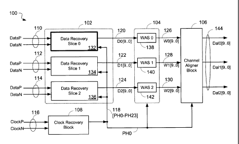
Figure 1 shows a block diagram of a HDMI receive interface 100 of the
embodiment of the present
invention. The HDMI receive interface 100 comprises a Data Recovery Block 102;
a Word Aligner
Block 104; a Channel Aligner Block 106; and a Clock Recovery Block 108. The
overall function of
the HDMI receive interface 100 is to recover the digital information sent to
it from an HDMI source
over a cable that includes 4 differential signal pairs.
The inputs to the HDMI receive interface 100 include three differential TMDS
(Transition
Minimized Differential Signaling) coded data channels 110, 112, and 114,
connected to the Data
Recovery Block 102, and a TMDS clock channel 116 connected to the Clock
Recovery Block 108.
The TMDS coding is described in the HDMI specification. As is conventional,
each differential
channel includes two signals: a positive and a negative signal, labeled DataP
and DataN respectively
for the data channels, and ClockP and ClockN for the clock channel.
A multiphase clock signal 118 (clock phases PHO to PH23 of the recovered
clock) is connected from
the Clock Recovery Block 108 to the Data Recovery Block 102. The clock phase
PHO is also
connected to the Word and Channel Aligners 104 and 106.
The Data Recovery Block 102 recovers the bit streams of the three TMDS coded
data channels 110,
112, and 114, and generates from them three 10-bit parallel digital signals
120, 122, and 124, labeled
DO[9..0], D1[9..0], and D2[9..0] respectively, for inputting to the Word
Aligner Block 104. The
function of the Word Aligner Block 104 is to align the three 10-bit parallel
digital signals (120, 122,
124) into three aligned data words 126, 128, and 130, labeled W0[9..0],
W1[9..0], and W2[9..01
respectively, for inputting to the Channel Aligner Block 106.
8
CA 02847649 2014-08-27
CA 2,847,649 Replacement Page RED-001-CA-DIV3
The Data Recovery Block 102 and the Word Aligner Block 104 are each comprised
of three
processing slices (Data Recovery Slices 0-2, reference numerals 132, 134, 136,
and Word Aligner
Slices [WAS] 0-2 reference numerals 138, 140, 142 respectively). Processing of
each of the three
TMDS coded data channels 110, 112, and 114 into the corresponding three 10-bit
parallel digital
signals 120, 122, and 124 is performed independently by the respective Data
Recovery Slices 132,
134, and 136, each of which also receives the multiphase clock signal 118.
Similarly, the processing of the three 10-bit parallel signals (120, 122, 124)
into the three aligned
data words 126, 128, and 130 is performed independently by the three
respective Word Aligner
Slices 138, 140, 142. Because of possibly different propagation delays (in the
cable from the signal
source, not shown) and processing delays in the Data Recovery Slices 132, 134,
136, and Word
Aligner Slices 138, 140, 142, the resulting three aligned data words 126, 128,
and 130 may arrive
skewed in time with respect to each other. The function of the Channel Aligner
Block 106 includes
aligning the three received digital channels (the aligned data words 126, 128
and 130) with each
other and provide a synchronized stream 144 of three 10-bit digital words to
subsequent processing
stages (not shown).
The Clock Recovery Block 108 converts the received TMDS clock channel 116 into
at least one
phase of the recovered clock 118; in the present invention, up to 24 recovered
clock phases (PHO to
PH23) are generated for use by the Data Recovery Block 102. The generation of
the multiphase
clock signal 118 from the TMDS clock channel 116 may be accomplished with a
phase locked loop
using any of a number of known techniques to generate multiple phases of a
clock, and is not
described in detail here.
The Word Aligner Block 104, and the Channel Aligner Block 106 are digital
processing circuits and
may be connected to only one of the recovered clock phases (e.g. PHO). These
digital processing
circuits are not further described.
The Clock Recovery Block 108 may be implemented as a common phase locked loop
(PLL) the
details of which are familiar to persons skilled in the art.
9
CA 02847649 2014-08-27
CA 2,847,649 Replacement Page RED-001-CA-DIV3
The HDMI receive interface 100 shown in Fig. 1 provides an exemplary context
within which the
present invention of a novel Data Recovery system is embodied. The Data
Recovery Slice 132 is
representative of the three Data Recovery Slices within the Data Recovery
Block 102. The following
descriptions provide more detailed information of the Data Recovery Slice 132.
Figure 2 shows an overview of the Data Recovery Slice 132 of the HDMI receive
interface 100,
including:
- an Analog Front End (AFE) 200 that comprises the following 5 blocks:
- a Level Shift block 202;
- a Differential Deskew block 204;
- an Equalization Block 206;
- a Differential-to-Single-Ended block 208;
- a Linear Phase Compensator 210;
and
- an Oversampling and Reclocking block 212;
- a Bit Extractor 214;
- a Word Assembler 216; and
- a Training Function block 218.
The TMDS coded data channel 110 comprising the differential signal (denoted
"DataP" and
"DataN") is an input to the Data Recovery Slice 132, and is connected to the
input of the Level Shift
block 202. The differential TMDS coded signal was (presumably) generated as a
digital signal by a
HDMI transmitter but may have suffered various forms of distortion, including
inter symbol
interference (ISI), delay and frequency distortion before it arrives as
effectively an analog signal at
the HDMI receiver 100. The first group of blocks (202 to 210), the so-called
Analog Front End
circuitry or AFE 200, are preprocessing stages that use analog techniques to
process the received
data signal in order to largely remove ISI and other distortions, and phase
align the data signal with
the clock before it (a preprocessed data signal) is oversampled in the
Oversampling and Reclocking
block 212 to be further processed as a digital signal using digital techniques
in the subsequent
CA 02847649 2014-08-27
CA 2,847,649 Replacement Page RED-001-CA-DIV3
blocks (214 to 218).
The Linear Phase Compensator 210 (having an analog delay line) is also
considered to be part of the
AFE 200. The single ended signal 226 is "analog" in the sense of timing, not
yet having been
retimed, even though it is full rail-to-rail, i.e. it has a "digital"
amplitude with sharp rise and fall
times.
It is worth noting for clarification, that although 24 clock phases are
provided, the spacing of the 24
clock phases is 1/12th of a data bit period. The 24 clock phases thus
effectively cover a period of
two data bits without however any presumption of clock/data alignment which
will be a function of
the Linear Phase Compensator 210 to be described below.
As also shown in Fig. 1, the multiphase clock signal 118 (comprising phases
PHO to PH23) provides
clocks for the Data Recovery Slice 132, specifically a clock reference (PHO)
to the Linear Phase
Compensator 210, a clocking signal (PHO) to the Word Assembler 216. All 24
phases of the
multiphase clock signal 118 (PHO to PH23) are connected to the Oversampling
and Reclocking
block 212.
The Level Shift block 202 generates a level shifted differential signal 220
that is input to the
Differential Deskew block 204 whose output is a differential deskewed signal
222. The differential
deskewed signal 222 is then processed by the Equalization Block 206 whose
output (an equalized
signal 224) is connected to the Differential-to-Single-Ended block 208 which
converts the equalized
signal 224 that is differential into a single-ended signal 226.
Both the Differential Deskew block 204 and the Equalization Block 206 receive
control signals
(deskew parameters 228 and equalization parameters 230 respectively) from the
Training Function
218.
The Linear Phase Compensator 210 receives as inputs the single-ended signal
226 and the PHO
phase of the multiphase clock signal 118, and produces as output a phase
aligned signal 232 (the
11
CA 02847649 2014-08-27
CA 2,847,649 Replacement Page RED-001-CA-DIV3
preprocessed data signal).
The Oversampling and Reclocking block 212 receives the phase aligned signal
232 as well as all 24
phases of the multiphase clock signal 118, to generate a 24-sample digital
samples signal 234 which
is then connected to both the Bit Extractor 214 and the Training Function
block 218. The output of
the Bit Extractor 214 is a single-bit signal 236 representing the processed
and recovered TMDS
coded digital bit stream, to be assembled into 10-bit words in accordance with
the HDMI
specification in the Word Assembler 216 that generates the 10-bit parallel
digital signal 120
(D0[9..0]) which is the output of the Data Recovery Slice 132.
The Training Function block 218 also receives the 24-sample digital samples
signal 234 which, as
will be described below, is used by this block to determine the deskew
parameters 228 and the
equalization parameters 230, that are then fed back to the Differential Deskew
and Equalization
Blocks (204 and 206) respectively.
Both the Word Assembler 216 and the Training Function block 218 also use one
of the clock phases
(PHO) of the multiphase clock signal 118.
The differential data (DataP and DataN) coming from the cable are immediately
passed through an
analog preprocessing section (the blocks 202 to 210, i.e. the analog front end
or AFE 200). One
purpose of the AFE 200 is to remove a large amount of the Inter-Symbol
Interference (ISI) and other
distortion in the data stream. The Differential Deskew block 204 and the
Equalization Block 206
will be described in more detail below. The data emerging from this section
(the preprocessed data
signal 232) is a single ended rail to rail signal with some residual ISI, and
whose phase has been
aligned to a clean on-board clock (the phase PHO of the multiphase clock
signal 118, derived from
the clock which is transmitted with the data, i.e. the TMDS clock channel 116,
Fig. 1). The phase
alignment is done by the Linear Phase Compensator 210, which does not use over-
sampling of the
data for phase detection (oversampling of the already aligned signal only
occurs in the next stage,
for a different purpose, see below). Rather, the Linear Phase Compensator 210
detects transitions in
the data signal (the single-ended signal 226) and uses an analog phase
detector and a delay circuit to
12
CA 02847649 2014-08-27
CA 2,847,649 Replacement Page RED-001-CA-DIV3
align the data with the clock (the phase PHO of the multi phase clock signal
118), as will be
described in more detail below. This block outputs the preprocessed data
signal (the phase aligned
signal 232) that is aligned to the onboard clock (PHO), and is followed by the
Oversampling and
Reclocking block 212 that uses multiple phases of the clock (PHO to PH23 of
the multiphase clock
signal 118) to create a digital representation of the preprocessed data signal
in the form of multiple
samples of the received wave form. The sampled data (24-sample digital samples
signal 234) is
then fed to the Bit Extractor 214 and the Word Assembler 216 to extract the
data bits and to combine
words of data (the 10-bit parallel digital signal 120) that are synchronized
with a slower word clock
(CLKWord, not shown).
Analog Front End (AFE) circuitry 200
The differential signal (the TMDS coded data channel 110) coming from the
cable may contain
significant Inter symbol interference (ISI) and other distortion. The
differential signal may also be
warped, that is the two signal components (DataP and DataN) are skewed in time
with respect to
each other (differential skew), further distorting the received signal. The
Differential Deskew block
204 and the Equalization block 206 process the differential signal, treating
it as an analog signal, in
order to compensate the differential skew and the ISI. The Linear Phase
Compensator 210 aligns the
data signal with the on-board clock PHO, to provide the preprocessed data
signal 232 to the next
stage (the Oversampling and Reclocking block 212).
The impact of differential skew is depicted in timing diagrams in Figures 3
and 4.
Figure 3a shows a timing diagram of the two single ended signal components
(V+, V-) of the
differential data on a HDMI channel, as it would be transmitted by an HDMI
source into the cable. A
timing diagram of the corresponding differential signal (Vdiff) is shown in
Figure 3b. The
differential signal is clean and easily interpreted.
Figure 4a shows an example timing diagram of the two single ended signal
components (V+ and
V-) of the differential data on a HDMI channel, as it might be received by an
HDMI receiver from
the cable. Figure 4b shows a timing diagram of the corresponding differential
signal (Vdiff). The
13
CA 02847649 2014-08-27
CA 2,847,649 Replacement Page RED-001-CA-DIV3
signals V+ and V- are skewed in time with respect to each other. The negative
signal component V-
is delayed with respect to the signal component V+ by a differential skew
delay of Td. As a
consequence, the differential signal (Vdiff in Fig. 4b) is significantly
distorted with clearly visible
plateaus in the signal where the differential signal is zero (0). These
plateaus regions can only be
interpreted as noise by the receiver, the result of which is to reduce the
width of the window of valid
data. This reduction is seen as closure of the receive data eye and directly
compromises the channel
quality. The amount of differential skew delay (Td) primarily depends on the
cable characteristics
and may include a small amount of differential circuit delays, but is
basically constant or varies only
slightly, slowly with time.
The differential skew delay may be compensated by inserting a delay element
having a delay of Td
in the path of V+ (in the case of the example of Fig. 4), or in the path of V-
in the opposite case
(where the input V+ signal was delayed with respect to V-), or neither if
there was no skew present.
Differential Deskewing 204
In the embodiments of the present invention, the differential skew is removed
(compensated) by the
Differential Deskew block 204 (Fig. 2), a simplified block diagram of which is
shown in Figure 5,
using the same reference numerals to indicate the differential inputs (220 and
222 respectively, each
with a positive [V+] and a negative [V-] terminal), and the control input for
the deskew parameters
(228).
The Differential Deskew block 204 shown in Fig. 5 includes a variable
(adjustable) delay 300 with a
(single ended) input 302 and an output 304, and six ON/OFF switches S1 to S6.
The variable delay
300 includes a number of delay stages 306. The switch S1 is connected between
the positive
terminal of the differential input (220 V+) and the positive terminal of the
differential output (222
V+). Similarly, the switch S6 is connected between the negative terminal of
the differential input
(220 V-) and the negative terminal of the differential output (222 V-). The
switches S2 and S4 are
connected between the input 302 of the adjustable delay 300 and the positive
(V+) and negative (V-)
terminals respectively of the input 220. Similarly, the switches S3 and S5 are
connected between the
output 304 of the adjustable delay 300 and the positive (V+) and negative (V-)
terminals
14
CA 02847649 2014-08-27
CA 2,847,649 Replacement Page RED-001-CA-DIV3
respectively of the output 222.
The scheme allows the single variable delay 300 to correct for both positive
and negative differential
skew. In effect, the single variable delay 300 is sufficient to compensate
positive or negative
differential skew (where either the positive signal or the negative signal is
delayed with respect to
the other), by switching it (the adjustable delay 300) into either the
negative or the positive signal
path respectively. For example, to pass the positive signal V+ through the
adjustable delay 300
(which is made of a cascade of delay units, to be described in detail below)
the switch states are as
follows: S1=OFF, S2=0N, S3=0N, S4=OFF, S5=OFF, and S6=0N. To pass V- through
the
adjustable delay 300 the switch states are as follows: S1=0N, S2=OFF, S3=OFF,
S4=0N, S5=0N,
S6=OFF. To switch the variable delay 300 out of both the V- and the V+ paths,
thus providing no
adjustment of the differential delay, the switch states are as follows: S1=0N,
S2=OFF, S3=OFF,
S4=OFF, S5=OFF, S6=0N.
It is contemplated that instead of inserting the composite delay into one the
other polarities of the
differential signal, it is possible to insert the composite delay into the two
polarities of the
differential signal.
There are two challenges to solve the deskew problem. The first is to make a
suitable delay, the
second is to tune the delay. Making the delay is a challenge, because the unit
should have a wide
enough bandwidth to pass the signals, but at the same time the block has to
produce a useful delay.
The wide bandwidth of a single delay stage naturally results in little delay,
so a cascade of stages is
required to achieve a sufficient delay.
A cascade of digital delay stages, including digital switches and a decoder to
provide binary
addressable selection of the overall delay, are described in United States
Patent 6,268,753. However,
the present invention requires an adjustable delay circuit to delay a high
speed analog signal.
Issues to be solved with a cascade of analog delay stages in the proposed
configuration of Fig. 5 for
differential skew compensation, include the need to provide unity gain, as
well as preserve the high
CA 02847649 2014-08-27
CA 2,847,649 Replacement Page RED-001-CA-DIV3
bandwidth required.
Among the prior art, several digital delay compensation schemes are disclosed,
but only few circuits
provide an adjustable delay for analog signals. For example, the use of a
follower circuit in parallel
with a gain stage to boost the high frequency response of a digital circuit is
taught in United States
Patent 5,739,713. United States Patent 6,525,568 teaches a phase shifting
(delay) stage that includes
an RC (resistor-capacitor) element followed by parallel gain stages of
nominally -1 and +2 gain,
their outputs added together to provide overall unity gain with a particular
complex frequency
transfer function. In the United States Patent Application 20050083130 a high
performance
amplifier is proposed which includes a delay element to compensate for signal
propagation delay
that may exist in alternative signal paths.
The preferred embodiment of the variable delay block 300 of Fig. 5, is shown
in Figure 6, as a
cascade of eight analog delay stages ("Delay Units") 306 in combination with
an analog selector
stage 308 is used to implement the adjustable delay 300. The eight delay units
306 are connected in
series (cascaded), the output of each delay unit 306 being input to the analog
selector stage 308. The
first delay unit 306 of the cascade provides the input of the variable delay
300 (IN 302).
The deskew parameters control signal (228) includes a 3-bit binary signal
connected to the analog
selector stage 308 for selecting one of its inputs to be switched through to
the output of the
adjustable delay 300 (OUT 304).
An exemplary complete circuit of the single delay unit 306 which may be
cascaded to provide a unit
of delay each, for the adjustable delay 300 is shown in Fig. 16 below.
To help in understanding the circuitry of the single delay unit 306, a step by
step description of the
issues to be solved, and possible solutions, is presented first.
To introduce the delay (Td) a simple RC delay circuit as shown in Figure 7 may
be used. The circuit
of Fig. 7 is a single ended circuit comprising a resistor R1, a capacitor C1,
and input and output
16
CA 02847649 2014-08-27
CA 2,847,649 Replacement Page RED-001-CA-DIV3
terminals (signals Vin and Vout), as well as a ground (0). The capacitor C1 is
connected between
Vout and ground, and the resistor is connected between Vin and Vout. Making a
circuit with an RC
delay as shown in Fig. 7 will succeed in delaying the signal but it will also
filter the signal. The
impact of the RC circuit of Fig. 7 on a pulse is seen from simulation results
shown in Figure 8. Fig.
8 shows two simulated wave forms, a trapezoid input pulse Vin, and an output
pulse (Vout), that
results from passing the trapezoid input pulse through the simple RC delay
circuit of Fig. 7. The
trapezoid input pulse (the signal Vin) is delayed and filtered (distorted)
into the output signal Vout.
The delay and the filtering action are clearly seen. While the delay is
desirable, the filtering action
causes dispersion and distortion of the pulse.
To reduce the filtering action of the circuit the RC time constant may be
reduced. The simulated
result is shown in Figure 9. The simulation shown in Fig. 9 is analogous to
the simulation shown in
Fig. 8, but with a reduced time constant in the simulated delay circuit.
Reducing the time constant
helps to increase or maintain the bandwidth (note the slopes of both the input
and output pulses) but
as shown in Fig. 9 the signal delay introduced is lower.
In the simulation of Fig. 9 the pulse width is 0.7 second and the RC time
constant in the circuit is
79ms. The long pulse duration and the long RC time constant were chosen merely
for convenience
in the simulations to study the effects of circuit choices, and are not
representative of the time scales
of the embodiment.
One method of attempting to regain the delay (as shown in Fig. 8 with respect
to the circuit of Fig. 7
with the original time constant) is to cascade a number of RC stages as shown
in Figure 10. Shown
in Fig. 10 is a delay circuit made from a cascade of three RC stages,
comprising the components R2,
C2, R3, C3, R4, and C4, preferably, each RC stage having individually the same
time constant of
79ms. The signals after the first and second stages are labeled V1 and V2
respectively. The input and
output of the circuit as a whole are labeled Vin and Vout.
The result of simulating the circuit of Fig. 10 with a trapezoidal input pulse
is shown in Figure 11
which shows the waveforms of the trapezoidal input pulse (Vin) and the
waveforms of the delayed
17
CA 02847649 2014-08-27
CA 2,847,649 Replacement Page RED-001-CA-DIV3
pulses after each stage of the circuit of Fig. 10 (V1, V2, and Vout). The
resulting final waveform
Vout is delayed but it is considerably reduced in amplitude and dispersed.
In order to remove the loading effect of subsequent stages, each stage may be
buffered as shown in
Figure 12. Shown in Fig. 12 is the same cascaded delay circuit as in Fig. 10,
but two buffers
(amplifiers) are inserted, a buffer "Bufl" between R1 and R2, and a buffer
"Buf2" between R2 and
R3. As a result, the intermediate signals V1 and V2 are not attenuated by the
loads of the
subsequent stages.
The simulation results for the circuit of Fig. 12 are shown in Figure 13. They
show that the circuit
arrangement of Fig. 12 achieves the desired goal of introducing significant
delay while the distortion
in the pulse is kept to a minimum. In this simulation the 0.7 second
trapezoidal input pulse is
delayed by approximately 77ms per stage.
In a mathematical sense, the pulse has been transformed by a cascade of single
pole unity gain
stages, the transfer function of each stage being;
H(s) 1/(1+s/p) where p[Rad = 1/(RC)
or p[HZ] is 1/(27cRC)
The goal of the circuitry is to delay the pulse by up to about half the pulse
width (bit width). In the
case illustrated in the simulation of Fig. 13, the required delay would be
approximately 0.35
seconds. To achieve this delay with the scheme shown in Fig. 12, this would
require approximately
five stages. In the simulation shown in Fig. 13 the RC time constant is set to
79ms which sets the
pole frequency at 1/(27E79ms) = 2Hz. Thus, with a pulse width of 0.7 seconds
(the input pulse Vin) a
stage with a pole frequency of 2Hz will produce suitable delays with
acceptable filtering on the
pulse. A simple approximation to calculate the position of the pole for a
system with a bit rate of N
bits per second (Nbps) is to set the pole in each stage at 3*N Hz. For
example, with a data rate of
1Gbps, a stage with a pole at approximately 3GHz would be needed.
18
CA 02847649 2014-08-27
CA 2,847,649 Replacement Page RED-001-CA-DIV3
Having shown how an appropriate delay per stage has been achieved using simple
RC stages, it
remains to be shown how a suitable buffer amplifier (Bufl, Buf2 in Fig. 12)
are constructed. To
make a unity gain buffer with unity gain up to 3GHz is a challenge even on an
advanced CMOS
processes. A starting point would be to use a simple follower circuit as shown
in Figure 14. The
simple follower circuit of Fig. 14 includes an N-channel MOS field-effect
transistor (MOSFET) M1
connected in series with a current source It The drain of the transistor M1 is
connected to ground
(0), while the positive terminal of the current source 11 connects to the
supply voltage VDD. The
circuit input (IN) is connected to the gate of the transistor M1, and its
source provides the circuit
output (OUT).
In this well known circuit, the output OUT follows the input IN with a gain of
approximately one.
The first limitation with this circuit is that the output is typically level
shifted by 0.3 volts or so. This
level shifting is a problem if a number of stages are to be cascaded, because
the successive level
shifts will cause the output to rise to the supply voltage and thus the signal
is clipped. To solve this
limitation, AC-coupling is added to the simple follower as shown in Fig. 15.
The circuit shown in
Figure 15 is an AC-coupled follower circuit, derived from the simple follower
circuit of Fig. 14 by
the addition of a capacitor C5 between the circuit input (IN) and the source
of the transistor M1, and
a resistor R5 between the source of the transistor M1 and a bias supply "BIAS"
that provides a bias
voltage.
With AC-coupling, the fact that the output of the stage is level shifted up
from the bias level set by
"BIAS" in Fig. 15 becomes unimportant when stages are cascaded, because this
level shift is stored
as a constant drop across the input capacitor of the next stage. This
essentially resets the average
input voltage at each stage to be the bias voltage set by the bias supply
(BIAS) shown in Fig. 15.
A further limitation of this circuit comes from the non-zero output
conductance of the transistor M1.
The gain of the follower is given by gml/(gml+gds1). Here "gml" is the small
signal
transconductance and "gdsl" is the small signal output conductance of M1.
Clearly, for all values of
"gdsl" greater than zero the gain of the stage is less than one. When fast
wideband circuits are
required, the length of the MOSFET M1 is reduced to close to minimum. This
causes "gdsl" to
19
CA 02847649 2014-08-27
CA 2,847,649 Replacement Page RED-001-CA-DIV3
increase to a point where the gain is now tending to 0.9 or so. A cascade of
these stages would
dramatically reduce the magnitude of the incoming signal.
One possible architecture, which corrects for this reduced stage gain is shown
in Figure 16
illustrating a simplified block diagram of a buffered delay stage 400, which
is an implementation of
the delay unit 306 of the adjustable delay 300 (Fig. 6).
The buffered delay stage 400 comprises a unit gain amplifier (buffer) 404. A
separate RC delay
element is not required in the high speed application as the delay is implicit
in the poles (limited
bandwidth) of the amplifier, and so indicated in the figure. The buffer 404,
having an input 410 and
an output 412, provides for isolating the delay element 402 from the next
delay element in the
cascade, as described earlier (Fig. 10).
The input 410 of the buffer 404 receives the input signal VIN of the buffered
delay stage 400 and the
output 412 of the buffer 404 generates the output signal VOUT of the buffered
delay stage 400.
The buffer 404 includes two amplifiers in parallel, a follower stage 414,
having a gain of
approximately 0.9 and a supplementary stage 416 with a gain of approximately
0.1, both amplifiers
having the same frequency response (expressed mathematically by the pole 1/(1-
f-s/p). Both
amplifiers (414 and 416) share the input 410 of the buffer 404, and their
outputs are summed into
the output 412.
The preferred embodiment of the buffer 404 including its component amplifiers
(the follower stage
414 and the supplementary stage 416), is shown in detail in Figure 17, as a
circuit based on an
N-well CMOS process.
The follower stage 414 is an AC-coupled circuit, similar to the AC-coupled
follower circuit of Fig.
15. It comprises a P-channel follower transistor M2, a biasing resistor R6, a
coupling capacitor C6,
and a bias supply "BIAS1".
20
CA 02847649 2014-08-27
CA 2,847,649 Replacement Page RED-001-CA-DIV3
The supplementary stage 416 includes a N-channel amplifying transistor M3, and
two P-channel
transistors M4 (functioning as a diode) and M5 (functioning as a current
source); a biasing resistor
R7; a coupling capacitor C7; a shunt capacitor C8; and a bias supply "BIAS2".
The bias voltages of "BIAS1" and "BIAS2" are adapted to the circuit functions
and the technology
as required.
The input 410 of the buffer 404 is connected through the coupling capacitor C6
to the gate of the
transistor M2, and through the coupling capacitor C7 to the gate of the
transistor M3. The positive
terminal of the bias supply "BIAS1" is fed to the gate of the transistor M2
through the biasing
resistor R6. Similarly, the positive terminal of the bias supply "BIAS2" is
fed to the gate of the
transistor M3 through the biasing resistor R7. The negative terminals of
"BIAS1" and "BIAS2", the
drain of the transistor M2, the source of the transistor M3, and one terminal
of the shunt capacitor
C8 are connected to ground. The other terminal of the shunt capacitor C8 is
connected to the gate of
the transistor M3. The source of the follower transistor M2 is connected to
the drain of the current
source transistor M5 and the output 412 of the buffer 404. The drains of the
transistors M3 and M4
are connected together, and also to the gate of the transistor M4. The sources
of the transistors M4
and M5 are connected to the supply voltage VDD.
Functionally, the signal of the input 410 of the buffer 404 is amplified by
the follower stage 414
with a gain of about 0.9, the transistor M5 (in the supplementary stage 416)
providing a current
source load to the transistor M2 of the follower stage 414. The function of
the supplementary stage
416 is to amplify a portion of the same input signal (the portion being
defined by the ratio of the
coupling capacitor C7 to the shunt capacitor C7) in the transistor M3 into a
varying current that is
mirrored through the transistors M4 and M5, and so providing a varying current
source load to the
follower transistor M2. Thus, both the follower stage 414 and the
supplementary stage 416
contribute to the signal at the output 412 of the buffer 404, their individual
contributions effectively
being added as indicated in Fig. 16 above.
The gain of the P-channel follower (414) is essentially unity except for the
output conductance (gds)
21
CA 02847649 2014-08-27
CA 2,847,649 Replacement Page RED-001-CA-DIV3
of the P-channel device (M2). Because of the requirement for speed a short P-
channel device is
required and thus the device has a large output conductance and the gain falls
toward 0.9. With a
cascade of 5 stages the signal would have fallen to 60% of its original value.
To boost the gain of the
simple follower at channel data rates, the parallel signal path is provided in
the form of the
supplementary stage 416.
As described above, the buffer 404 includes a second path (the supplementary
stage 416) for the
input signal (410) to arrive at the output 412. This extra path is through C7,
M3, M4, and M5. In this
path, the high frequency input signal is passed though C7 and a fraction of
the signal is presented at
the gate of M3. This fraction is changed by changing the size of the shunt
capacitor C8. The current
in M3 is set to a nominal value with a bias circuit ("BIAS2"). When the input
signal arrives at the
gate of M3 it varies the current in M3. This current variation is sourced by
the diode connected
device (M4) which then mirrors the current change to M5. Finally M5 changes
the current in M2 so
the end result is that changing the input signal changes the current in M2.
Changing the current level
in M2 changes the overdrive in the device and thus changes the output voltage.
In summary, a
positive change at the input 410 causes a positive change at the output 412
due to current steering in
the parallel path. At the same time there is a positive change at the output
due to the simple follower
action through M2. The overall change in the output is calculated by summing
the contributions
from the Parallel (supplementary stage 416) and Main (follower stage 414)
paths. If the main path is
producing a gain of 0.9 the parallel path may be tuned to provide a gain of
0.1 by changing the value
of C8. Once adjusted to unity, the gain of the stage remains stable over
Process, Supply Voltage, and
Temperature to within about two percent of its nominal value.
The buffer circuit 404 of Fig. 17 meets the following requirements.
= An overall gain of unity, and thus cascading does not amplify or reduce the
signal;
= Capable of very wideband operation (pole at 2GHz to lOGHz) for minimal
distortion; and
= Input and Output levels of a cascade of stages stay within a suitable
range.
Some typical values for the implementation of the buffer 404 are:
R6=200k, R7=200k, C6=200f, C7=200f, C8 in the range of about 400f tuned to
adjust the overall
22
CA 02847649 2014-08-27
CA 2,847,649 Replacement Page RED-001-CA-DIV3
gain of the circuit to unity.
An implementation of the buffer, equivalent to the buffer circuit 404 shown in
Fig. 17, is created by
starting with a simple N-channel follower (instead of the P-channel follower
of Fig.14, that has led
to the complete buffer implementation shown in Fig. 16). The simple N-channel
follower is shown
in Figure 18.
For a CMOS process with a P-Well technology the configuration shown in Fig. 18
would be the
preferred implementation in that the bulk of the N-channel MOSFET would be
free to be tied to the
source as shown in Fig. 18. For the more standard CMOS processes with N-Well
technology the
circuit of the buffer of Fig. 18 would cause additional challenges because the
bulk connection on the
N-channel MOSFET is tied to ground. This grounded bulk causes a varying source-
to-bulk potential
in the transistor and further degrades the gain of the stage from 0.9 and this
reduced gain makes it
more difficult to maintain the overall gain of the stage at unity.
Another implementation of the buffer stage for the delay stage 306 is shown in
Figure 19, which
shows a modified buffer 404B. The modified buffer 404B is similar to the
buffer 404 and also uses
two parallel paths for the input (410) to output (412) signal, i.e. the
follower stage 414 and a
modified supplementary stage 416B. The modified supplementary stage 416B
performs the same
function as the supplementary stage 416, but is implemented somewhat
differently.
The supplementary stage 416B comprises five N-channel transistors (M6, M7, M8,
M9, and M10)
and two P-channel transistors (M11, M12), a biasing resistor R8, a coupling
capacitor C9, a shunt
capacitor C10, and a current sink 12.
The components of the supplementary stage 416B are variously connected to each
other, ground,
and VDD as listed in the following:
- the sources of the N-channel transistors (M6 to M10) and one lead of the
shunt capacitor C10 are
connected to VDD;
- the sources of the P-channel transistors (M11 and M12) as well as the
negative terminal of the
23
CA 02847649 2014-08-27
CA 2,847,649 Replacement Page RED-001-CA-DIV3
current sink 12 are connected to ground;
- the transistors M6, M9, and M11 are each connected in diode mode, i.e. their
gates are shorted to
their drains;
- the drain/gate of the transistor M6 is connected to the positive terminal of
the current source 12, the
gate of the transistor M7, and through the biasing resistor R8 to the gate of
the transistor M8;
- the drain of the transistor M7 is connected to the drain/gate of the
transistor M11 and to the gate of
the transistor M12;
- the gate of the transistor M8 is further connected to the shunt capacitor
C10, and through the
coupling capacitor C9 to the input signal (410);
- the drain of the transistor M8 is connected to the drain/gate of the
transistor M9, to the gate of the
transistor M10, and the drain of the transistor M12; and lastly
- the drain of the transistor M10 is connected to the drain of the transistor
M2 of the follower stage
414 as well as the output 412.
In this configuration (the supplementary stage 416B), the circuitry formed by
the current sink 12 and
the transistor M6 provides a bias voltage (from which, through the resistor
R8, the operating point of
the transistor M8 is set; and further, through the current mirror formed by
M11 and M12, the current
drawn by the transistors M8 and M9 is set.
The input signal (410) fed through the coupling capacitor C9 to the gate of
the transistor M8
modifies the current in the transistor M8 and thus modifies the current in the
transistor M9 (the
current in M9 is the difference between the constant current set in M12 and
the signal dependent
current in M8), and consequently the current in the transistor M10 due to the
mirroring of M9 and
M10. The variation of current in the transistor M10 which is in series with
the transistor M2 in the
follower stage 414, has the same effect as that described earlier for the
variation in the equivalent
transistor M5 of the original supplementary stage 416.
Again, a configuration similar to the circuitry of the buffer 404B may be
produced if one starts with
an N-channel follower as shown in Fig. 18 above.
24
CA 02847649 2014-08-27
CA 2,847,649 Replacement Page RED-001-CA-DIV3
Equalization 206
The output of the cable shows a low pass filtered response and thus there is
significant distortion to
the incoming signal. The challenging features of the distorted signal are
reduced rise times and the
fact that a single data bit change does not cause the signal to traverse the
signal range.
Figure 20 shows typical waveforms at the input and the output of a cable, for
illustration of this
common problem. The limited bandwidth of the cable suppresses the high
frequency components of
the data signal. A simplified transfer function of a cable illustrated in
Figure 21 shows the reduction
in gain at high frequencies.
The high frequency suppression is conventionally solved by placing an
equalizer in the receiver. The
equalizer provides an increased gain at the higher frequencies so the
cascading of the transfer
functions results in a flat unity gain transfer function over the frequencies
of interest as shown below
in Figure 22.
This existing approach to solving the problem is described, e.g. in a US
patent number 6,819,166.
This existing implementation describes an equalizer with a variable transfer
function, and a method
of detecting the level of high frequency suppression in the cable such that
the equalizer can be tuned
to accurately offset the impact of this.
In the embodiment of the present invention, a tunable equalizer is provided in
the Equalization block
206 (Fig. 2). Instead of providing infinitely variable equalization, only
three discrete settings (low,
medium, and high) are implemented, which may be selected under control of the
equalization
parameters 230. In combination with the ability to provide differential
deskewing of the signal (see
Differential Deskew block 204, Fig. 5 above), this amount of equalization
control has been found
sufficient for the intended first application in an HDMI receiver. Other
applications may require
finer control.
Analog Phase Recovery (Linear Phase Compensator 210)
After being converted to the single-ended signal 226 in the Differential-to-
Single-Ended block 208
CA 02847649 2016-03-10
CA 2,847,649 Replacement Page RED-001-CA-DIV3
(see Fig. 2), the data is now ready to be sampled to extract the data. The
problem, however, is that
the phase of the data relative to the sampling clock is unknown. When this
phase relationship is
unknown, there is a danger of sampling during data transitions and
misinterpreting the data in the
data stream. To define the phase relationship between the on-board clock (PHO
of the recovered
multi-phase clock 118) and the data (the single ended signal 226), an Analog
Phase detector (within
the Linear Phase Compensator 210) is used. The frequency of the data and the
onboard clock are
equivalent because the timings in both are derived from the same source, that
is, the transmitted
clock, so there is no need for frequency adjustment. The Linear Phase
Compensator 210 employs a
scheme similar to that described in the paper entitled "A 10-Gb/s Clock
Recovery Circuit with
Linear Phase Detector and Coupled Two-stage Ring Oscillator" by Afshin Rezayee
and Ken Martin.
This paper was published at the European Solid State Circuits Conference
(SSCIRC) in Florence,
Italy in the year 2002, pp. 419-422.
In this phase detection scheme of Rezayee and Martin, a window in time is
generated around rising
edges in the data stream. The phase detector is only enabled within this
window. The window is of
such a length that one clock edge is guaranteed to be present, but only one.
In the Rezayee & Martin
implementation, the clock and data are locked such that clock edges occur in
the middle of the data
bits. This allows the aligned clock to sample in a region where the data is
stable.
In the implementation of the phase detector circuit described herein, the
Linear Phase Compensator
210 aligns the clock and data edges. The resulting phase aligned data signal
(the phase aligned
signal 232) is subsequently over-sampled in a separate circuit block (The
Oversampling and
Reclocking block 212) before determining the bit value (in the Bit Extractor
block 214).
A block diagram of an exemplary implementation 500 of the Linear Phase
Compensator 210 is
shown in Figure 23.
The Linear Phase Compensator 210 (the implementation 500) comprises:
- a Programmable Analogue Delay 502 having a data input (Din) and a control
input (Cin);
and an Analog Phase Detector (APD) 503, which includes:
26
CA 02847649 2014-08-27
CA 2,847,649 Replacement Page RED-001-CA-DIV3
- a Window Generator 504;
- a Phase Detector 506 having a clock input "Ck", a data input "Data", and
an enable input EN;
- and a Charge Pump 508 with inputs "Up" and "Down", and including a
capacitor C11.
The inputs to the Linear Phase Compensator 210 are the data signal (the single
ended signal 226),
and the clock signal (the PHO of the recovered multi-phase clock 118). The
data signal is connected
to the data input (Din1) of the Programmable Analogue Delay 502, the output of
which is the phase
aligned signal 232 (the preprocessed data signal). This signal (232) is
further connected to the input
of the Window Generator 504 and to the enable input "EN" of the Phase Detector
506. The clock
input "Ck" of the Phase Detector 506 receives the on-board clock, that is the
phase 0 (PHO) of the
multi phase clock signal 118 (see Fig. 2). The outputs of the Phase Detector
506 drive the "Up" and
"Down" inputs of the Charge Pump 508. The output of the Charge Pump 508 is an
analog control
signal, connected to the control input Cin of the Programmable Analogue Delay
502.
The Window Generator 504 detects positive edges on the input data and
generates the enable (EN)
signal for the Phase Detector 506, of duration guaranteed to contain an edge
of the clock to which
the data is to be locked.
The Phase Detector 506, uses the enable signal (EN), supplied by the Window
Generator 504, to
compare the phases of the "Data" and "Ck" signals during the length of the
enable signal (EN). The
outputs of the phase detector control the Programmable Analogue Delay 502, by
means of the
Charge Pump 508 which is a control voltage generator, generating a control
voltage by charging the
capacitor C11 or by other suitable means.
The Programmable Analogue Delay 502 takes the control signal from the phase
detector (the control
input "Cin") and delays the data signal by a programmable amount to align it
with the clock signal.
The output of the Programmable Analogue Delay 502 is thus the phase aligned
signal 232.
This Linear Phase Compensator 210 (implemetation 500) works robustly in the
presence of ISI
(Inter-Symbol Interference) and jitter and aligns the on-board clock edges
with the substantially
27
CA 02847649 2014-08-27
CA 2,847,649 Replacement Page RED-001-CA-DIV3
"ideal" data transition points in the data channels.
Bit Extraction 214 and Word Assembly 216
The phase aligned (data) signal 232 is a rail-to-rail analog signal that may
still contain ISI,
distortion, noise, and other impairments. In the Oversampling and Reclocking
block 212 (Fig. 2),
this signal is effectively sampled at a rate 12 times the clock rate of the
signal, i.e. during each bit
period the data signal is sampled at 12 evenly spaced intervals, to generate
12 digital samples.
Because of the high speed of the signal (1.65 Gbs) it is not practical to
actually sample the signal
with a 12-times higher clock signal. Instead, the same effect is achieved by
sampling the signal with
12 evenly spaced phases of the clock signal, each clock phase generating a
digital sample, thus 12
samples representing one data bit. In the present embodiment, 24 clock phases
(PHO to PH23 of the
multiphase clock signal 118) are used to capture not only one data bit in 12
sampling phases, but
also the trailing half of the previous data bit in 6 sampling phases and the
leading half of the next
data bit in another 6 sampling phases (conventional digital register logic and
pipelining is used to
thus look into the "future").
Because of the oversampling, the term "bit" might become ambiguous. The terms
"bit", "primary
data bit", and "bit-clock period" will be used to denote the nominal 1.6 Gbs
data bits and their
period; "sample" and "sample bit" to denote one of the 12 samples per bit-
clock period; and
"24-sample word" to denote the ensemble of 24 samples, as described.
Thus the Oversampling and Reclocking block 212 generates 24 samples (a "24-
sample word") at the
bit-clock rate, by outputting the 24-sample digital samples signal 234.
Figure 24 illustrates data phase shifting in the Programmable Analogue Delay
502 of Fig. 23, and
oversampling in the Oversampling and Reclocking block 212 of Fig. 2. The
diagram 600 in Fig. 24
that shows an exemplary waveform 602, a delayed waveform 604, a set of
sampling clocks 606, a
24-sample word 608, and a scale indicating a bit-period and previous and next
bits.
The exemplary waveform 602 represents an example of the single ended signal
226 (Fig. 2) before
28
CA 02847649 2014-08-27
CA 2,847,649 Replacement Page RED-001-CA-DIV3
phase alignment. Note that the signal appears to be a "1" bit with some
distortion (noise or ISI) near
the one-zero transition, and it is not aligned with the indicated bit-period.
The delayed waveform
604 represents the corresponding phase aligned signal 232 after delay through
the Programmable
Analogue Delay 502. Note that the signal is now approximately aligned with the
indicated
bit-period, but still includes the distortion. This signal is sampled with the
24 phases of the
multiphase clock 118 (PHO to PH23) as indicated by the set of sampling clocks
606 in the
Oversampling and Reclocking block 212, resulting in the 24-sample word 608.
The 24-sample word
608 includes six samples (000000) from the previous bit period, twelve samples
(111111111100)
from the Bit-period and another six samples (000000) from the next bit period.
The 24-sample word 608 is output by the Oversampling and Reclocking block 212
as the 24-sample
digital samples signal 234 to the Bit Extractor block 214 (Fig. 2) as well as
to the Training Function
218.
In the Bit Extractor block 214 the 24-sample digital samples signal 234 is
analyzed to determine
probabilistically if the present data bit (represented in the phase aligned
signal 232 and sampled at
24 points) is a logic "0" or a logic "1". While this could be achieved with a
simple majority voting
circuit, the following more elaborate algorithm is used in the preferred
embodiment of the invention.
The method searches for the bit in the middle twelve samples, but also in
samples either side of this
midsection (hence the requirement for six "previous bit" samples and six "next
bit" samples).
Sample-to-sample jitter can move the bit forward and back relative to the
clock, even when on
average it is correctly aligned. The approach taken to declaring that the bit
is a logic "1" or logic "0"
is to accept short bits ¨ down to 5 samples long in the present implementation
¨ if they are located
centred on the expected bit centre. Longer runs of samples are accepted even
if they are further from
the expected centre ¨ this is where the samples from the previous bit and next
bit are used.
More precisely, in the present implementation we accept a run of 5 contiguous
"1" or "0" samples
located within a window of 6 centred on the expected bit centre as a "1" or
"0"; for runs of length 6
samples, the window is 10 wide; for runs of 7 samples, the window is 12 wide;
for runs of 8
29
CA 02847649 2014-08-27
CA 2,847,649 Replacement Page RED-001-CA-DIV3
samples, the window is 14 wide; for runs of 9 samples, the window is 16 wide;
and for 10 or more
samples it is 18 wide.
Eye quality tuning (Training Function 218)
The Training Function 218 (Fig. 2) provides feedback from the 24-sample
digital samples signal
234, which is a stream of 24-sample words such as illustrated in the 24-sample
word 608 of Fig. 24,
to the analog front end (AFE 200) in order to tune the adjustable parameters
of the AFE.
The approach taken in the preferred embodiment of the invention is to once at
startup (or upon any
other trigger) systematically go through each of the possible permutations of
settings of these
parameters; observe and measure the quality of the preprocessed signal 232
oversampled as the
24-sample digital samples signal 234 point (obtain a quality measure in the
form of a "Quality
Number"); and retain the setting which results in the best Quality Number
obtained.
The AFE settings may include (actual values in the example embodiment are
shown in brackets,
based on the bit oversampling factor of 12):
- settings of differential delay compensation (7 values, ranging from about
0 to approximately 360
psec);
- insertion of the differential delay in the positive or negative polarity
signal (positive or negative);
- frequency response (cable) equalization settings (low, medium, high);
for a total of number of permutations of (7 x 2) x 3 = 42.
Note that the bit-clock to data-bit phase offset setting is not of interest
here, being independently
adjusted by the Linear Phase Compensator 210. The phase aligned data signal
232 will be fairly
accurate in phase, that is centering the nominal bit-period on the middle
twelve samples of the
24-sample word, provided the AFE settings are within the vicinity of the
optimal settings. If they
are not, it does not matter if the data/clock phase alignment is suboptimal.
Implementation of the Training Function 218
A simplified block diagram of the preferred embodiment 700 of the Training
Function 218 is shown
CA 02847649 2014-08-27
CA 2,847,649 Replacement Page RED-001-CA-DIV3
in Figure 25.
The Training Function 700 includes the following blocks:
- a Bit Length Detection block 702;
- a set of Length-i counters (i = 5 to 12), designated by reference numerals
704 to 718;
- a Bit Quality Calculator 720 including a Best Quality Number register
722;
- a Best Settings Memory 724 having inputs D and W, and an output Q;
- a write-enable gate EN 726;
- a Current Settings Memory 728;
- an Evaluation Run Control block 730; and
- a selector MUX 732.
The inputs to the Training Function 700 are the 24-sample digital samples
signal 234 that is
connected to the Bit Length Detection block 702, and the board clock (PHO of
the multiphase clock
signal 218). The output of the Bit Length Detection block 702 is a set 734 of
count-enable signals,
one count-enable signal connected to each of the Length-i counters 704 to 718.
The outputs of each
of the Length-i counters 704 to 718 provide inputs to the Bit Quality
Calculator 720. The Bit Quality
Calculator 720 in turn is connected with a "save best settings enable" control
signal 736 to the
write-enable gate EN 726. The other input of the write-enable gate EN 726
receives an
"end-of-calculation" signal 738 from the Evaluation Run Control block 730. The
output of the
write-enable gate EN 726 is connected to the write control input "W" of the
Best Settings Memory
724. The output Q of the Best Settings Memory 724 sends a multi-bit "best
settings" signal 740
which is a digital control word indicative of AFE settings values. The "best
settings" signal 740 is
connected to one of the two data inputs of the selector MUX 732 whose other
data input receives a
similar data word, i.e. a "current settings" signal 742 from the Current
Settings Memory 728. The
"current settings" signal 742 is also applied to the data input D of the Best
Settings Memory 724.
The outputs of the Evaluation Run Control block 730 include the "end-of-
calculation" signal 738
connected the write-enable gate EN 726 (already mentioned above), and an "end-
of-search" signal
744 connected to the select input of the selector MUX 732. The output of the
selector MUX 732
(outputting either the "current settings" 742 or the "best settings" 740
depending on the state of the
31
CA 02847649 2014-08-27
CA 2,847,649 Replacement Page RED-001-CA-DIV3
"end-of-search" signal 744) is split into the deskew parameters 228 and the
equalization parameters
230 that are fed back to the Differential Deskew (204) and Equalization (206)
blocks respectively,
see Fig. 2.
The overall operation of the Training Function 700 is controlled by the
Evaluation Run Control
block 730 which, briefly noted, allows the analog front end (AFE) to run (an
"evaluation run") for a
specific period of time (corresponding to a large number N of received data
bits) at each of the
predefined sets of AFE parameter settings ("current settings"). Each
"evaluation run" of the Training
Function 700 runs for a duration equivalent to the N primary data bits (an
observation period of "N"
bits). A "training run" is the sequence of "evaluation runs", each with a
different set of "current
settings". The purpose of the "Training Function" is to select the permutation
of AFE settings that
gives the "best" (highest) Quality Number, and retain these settings for the
subsequent operation of
the HDMI receiver. The Training Function may be invoked (started) once after
power-up. It may
also be invoked periodically to allow for drift, equipment connect/disconnect,
and other factors.
While the Training Function 218 is the primary means to set the AFE parameters
based on the
Quality Number obtained with the "Bit Quality Calculator" 720, the AFE
parameters may not be
updated regardless of the Quality Number if the word alignment logic fails to
synchronize. The
operation of the "training run" is further described with the help of a flow
chart (Fig. 26 below). The
functions of the individual blocks of the Training Function 700 shown in the
Fig. 25 are briefly
explained first.
The Bit Length Detection block 702 receives the 24-sample digital samples
signal 234 indicating an
oversampled received bit (nominally in the middle 12 samples) and samples of
adjacent bits, as
described above (Fig. 24), and treating it as a digital word of 24 bits
(samples); and detects within
each such digital word clusters (runs) of adjacent "ls", bracketed by at least
one "0" sample at each
end. For example the 24-sample word 608 of Fig. 24 "000000111111111100000000"
contains a run
of ten "1s" samples. The function of the Bit Length Detection block 702 is to
classify each arriving
24-sample word 608 by the lengths of the "ls" run (if any) contained in it and
increment the
corresponding Length-i counter (704 to 718) accordingly. In the example above
the Length-10
counter 714 would be incremented.
32
CA 02847649 2014-08-27
CA 2,847,649 Replacement Page RED-001-CA-DIV3
Note that there are no counters for lengths below 5 or above 12; these lengths
are ignored.
The Length-i counters 704 to 718 thus, record and accumulate the number of
occurrences of the
corresponding run lengths of "ls" in the stream of 24-sample words in the
digital samples signal
234, for each evaluation run.
At the end of each evaluation run, the outputs of the Length-i counters 704 to
718 are fed into the
Bit Quality Calculator 720 which computes a Quality Number from the ensemble
of accumulated
length counts according to a heuristic algorithm. Recall that the purpose of
"training" the analog
front end is to find the "best settings", that is the settings which results
in the most appropriate
equalization setting (see the Equalization block 206, Figs. 2 and 22) and
which "optimally" removes
any differential skew that might exist by adjusting the Differential Deskew
204. An ideal data signal
of alternating "1s" and "Os", that was perfectly phase aligned (see Linear
Phase Compensator 210,
Fig. 23) would after oversampling result in successive 24-sample words of:
000000111111111111000000
111111000000000000111111
and result in high counts for the run length 12. The runs of length 6 would
not be counted, as only
contiguous runs of "1" samples with "0" samples on either side of the run are
counted. Thus, the six
samples located at the end of the window are not counted ¨ they're part of a
bit that was or will be
counted in the previous or subsequent bit period respectively.
If the signal shape was perfect (twelve "1" samples per bit) but phase
alignment was skewed by one
or a few samples, the result would be that the same high counts for the run
length 12 would be
recorded. If the signal was distorted (imperfect differential deskewing, high
ISI, or non-optimal
equalization setting), other lengths may be recorded.
33
CA 02847649 2014-08-27
CA 2,847,649 Replacement Page RED-001-CA-DIV3
At the end of an evaluation run the Quality Number is computed by the Bit
Quality Calculator 720,
by multiplying the contents of each Length-i counter 704 to 718, with a length
specific weight, and
summing the products:
for i=5 to 12,
Bit Quality Number = SUM(Lengthi count x Weighti)
The following set of weights have been used in the embodiment of the
invention, but other weights
may also give good results:
Weight5 = -2
Weight6 = -2
Weight7 = -1
Weight8 = 1
Weight9 = 1
Weight10 = 2
Weight11 = 4
Weight12 = 8
The selected weight numbers suggest, as may be expected, that a run length of
12 being indicative of
a perfect pulse has the highest weight, while run lengths below 8 may be
indicative of severe
distortion, resulting in a negative contribution to the Bit Quality Number.
The Bit Quality Number from each evaluation run with a particular set of AFE
settings (the current
settings) is compared with the currently stored Best Quality Number (in the
register 722). If it
exceeds the previous Best Quality Number, the Best Quality Number 722 is
updated with the higher
number, and the current settings is saved in the Best Settings Memory 724.
This functionality is
indicated in Fig. 25 where the output of the Bit Quality Calculator 720 (the
"save best settings
enable" control signal 736) is ANDed with the "end-of-calculation" signal 738
from the Evaluation
Run Control block 730 in the write-enable gate EN 726 to generate a write
signal ("W" input) for the
34
CA 02847649 2014-08-27
CA 2,847,649 Replacement Page RED-001-CA-DIV3
Best Settings Memory 724 while at the same time, the current settings (the
"current settings" signal
742 from the Current Settings Memory 728) is presented at the data input "D"
of the Best Settings
Memory 724, causing it to store the current settings.
If on the other hand with a given current settings, a Bit Quality Number is
obtained that is not higher
than the Best Quality Number already stored in the register 722, the write-
enable gate EN 726 is not
enabled, and the current settings is not stored in the Best Settings Memory
724.
The Evaluation Run Control block 730, for each evaluation run, chooses a
current settings
permutation and stores it in the Current Settings Memory 728 for the duration
of the each evaluation
run. During each evaluation run, the "current settings" 742 are fed through
the selector MUX 732 to
provide the deskew and equalization parameters (228 and 230).
After all permutations are exhausted, that is at the end of the "training
run", the "end-of-search"
signal 744 is asserted by the Evaluation Run Control block 730 which then
causes the selector MUX
732 to send the "best settings" into the deskew and equalization parameter
signals (228 and 230).
In the present embodiment of the invention, the number of received data bits N
for which each
evaluation run is held, is 65536. Due to present technology limitations, the
blocks 702 to 718 of the
Training Function circuit 700 are duplicated (duplication not shown in Fig.
25). Each of these
blocks operates at half speed, processing the 24-sample digital samples signal
234 for alternate
received data bits with the Bit Quality Number simply computed at the end of
each evaluation run
from the contents of the Length-i counters of both sets of counters. Thus in
effect, a total of 2N =
131072 bits are processed for each evaluation run, and with the chosen set of
AFE parameters (42
permutations, see above) 42 evaluation runs are made for one training run. At
a data rate of 1.6Gbs,
the complete training run thus occupies a period of approximately 4 msec,
which is short enough to
justify the approach taken here, that is to systematically try all
permutations and retain the best. If
substantially more parameters were to be included and many more permutations
were possible, then
more complex search strategies could be applied to shorten the training
period.
35
CA 02847649 2014-08-27
CA 2,847,649 Replacement Page RED-001-CA-DIV3
Alternative implementations of the Training Function 218 are also envisaged
which may differ in the
details from the embodiment 700. For example, the number of clock phases for
oversampling the
received data signal may be less or more than 24, and the window of
oversampling may include at
least one bit period (the middle samples), but be narrower or wider with
respect to adjacent bits.
Instead of counting run lengths of "1" samples, run lengths of "0" samples may
be accumulated, and
different weightings may be applied to the run length counts. These and other
variations that may
occur to skilled persons are included in the scope of the invention.
In Figure 26 is shown a high level flow chart of a training run 800, depicting
the operation of the
Training Function 218 (corresponding to the embodiment 700 of Fig. 25). The
training run 800 is a
finite process that may be invoked to run from "Start" to "Finish" through a
number of steps that are
either actions or logic decisions:
802: "Reset the best Quality Number (bestQN)";
804: "Get the first current Settings";
806: "Do an Evaluation run";
808: "Compute a Quality Number (QN)";
810: "Is the computed Quality Number greater than the best Quality
Number (QN > bestQN)?", Yes or No;
812: "Set the best Settings to the current Settings, and
set the best Quality Number to the computed Quality Number
(bestSettings := currentSettings; bestQN := QN);
814: "Is Training Finished ?", Yes or No;
816: "Get the next current Settings"; and
818: "Send the best Settings to the Analog Front End (AFE)".
The current Settings refers to the parameters that may be controlled in the
analog front end (AFE
200). At the start of the training run, a stored variable "best Quality
Number" (bestQN) is initialized
("reset bestQN" 802) and a first set of the AFE parameters is created ("Get
first currentSettings"
804). This is followed by a loop over the steps 806 ("Do an Evaluation run")
to 816 ("Get the next
36
CA 02847649 2014-08-27
CA 2,847,649 Replacement Page RED-001-CA-DIV3
current Settings") which is executed until all settings (permutations of the
AFE parameters) have
been exhausted and training is finished, as indicated by the step 814 ("Is
Training Finished ?"). The
training run 800 ends with the step 816 ("Send the best Settings to the Analog
Front End").
Within the loop (steps 806 to 816), the step 806 ("Do Evaluation run") is
followed by the step 808
("Compute a Quality Number") which computes the Quality Number from the
results of the
evaluation run. This step 808 may be performed by the Bit Quality Calculator
720 of Fig. 25, for
example. In the next step 810 "Is the computed Quality Number greater than the
best Quality", a
comparison is made between the last computed quality number (QN) and the
stored "best Quality
Number" (bestQN). If QN is greater than bestQN then the current settings is
assigned and stored in a
variable "best Settings", and also the stored variable "bestQN" is updated
with the last computed QN
(the step 812). In the step 814 "Is Training finished?", it is determined if
all valid permutations of
the AFE parameters have been evaluated. If training is NOT finished, the next
permutation is
created in the step 816 "Get next current settings", and the loop continues
with the evaluation run
(step 806). If there are no more permutations to evaluate, training is
finished ("Yes" in the step 814
"Is Training finished ?"), the current settings are abandoned, and the best
Settings are sent to the
analog front end in the step 818, before the training run 800 exits.
The Evaluation run of the step 806 is further detailed in a subroutine flow
chart of an exemplary
evaluation run method 900 that is shown in Figure 27.
The evaluation run 900 runs from "Enter" to "Return" through a number of steps
that are either
actions or logic decisions:
902: "Send the current Settings to the analog front end (AFE)";
904: "Reset the Length[i] counters";
906: "Get the next oversampled bit";
908: "Compute the run lengths (RL)";
910: "for each i for which RL[i] is not 0, increment the Length[i] counter";
and
37
CA 02847649 2014-08-27
CA 2,847,649 Replacement Page RED-001-CA-DIV3
912: Is Evaluation run finished ?".
The current settings (see the flow chart of the "Training run" 800) are sent
to the analog front end
(AFE) in the step 902, and remain constant for the duration of the evaluation
run 900. The run is
initialized by resetting all Length counters to 0 in the step 904. These
counters correspond to the
Length counters 704 to 718 of the embodiment 700 (Fig. 25). Only counters for
i = 5 to 12 (selected
run length 5 to 12) are provided in the present embodiment of the invention,
but other ranges may be
used, especially if oversampling of the data bits is by a factor different
than the factor 12 as in the
present embodiment.
The next oversampled data bit and adjacent samples is obtained in the step
906. This "Oversample"
corresponds to the 24-sample digital samples signal 234 of the earlier
description (Figs. 2 and 24).
In the next step 908 ("Compute run lengths"), the received oversample is
analyzed to determine run
lengths of "1s" as described earlier (the Bit Length Detection 702, Fig. 25).
This step produces an
indication for each run length (only run lengths of 5 to 12 are covered) that
is found in the
oversample. In the next step 910 ("for each i for which RL[i] is not 0,
increment the Length[i]
counter"), each Length[i] counter for which a run length was indicated in the
previous step is
incremented.
The end of the evaluation run is indicated in the step 912 "Is Evaluation run
finished?" if a sufficient
number of data bits (oversamples) have been processed, (in other words, a
simple loop count is
maintained, and after for example 65536 loopings), the evaluation run exits,
that is it returns to the
next step 808 in the training run 800 where the contents of the Length
counters are converted into
the Quality Number.
The quality measure of the channel, as expressed in the Quality Number, can be
used to tune any
parameter in the system, the only limitation being that adding a parameter to
be tuned adds to the set
up time of the channel.
While an embodiment of a specific training function (700) has been presented
in detail, it is
38
CA 02847649 2014-08-27
CA 2,847,649 Replacement Page RED-001-CA-DIV3
understood that other training functions are within the intended scope of the
invention, i.e.
performing a real time analysis of the preprocessed data signal in order to
find an optimal or near
optimal set of parameters for adjusting the AFE for better performance in
reducing ISI and other
analog signal impairments.
Although the embodiment of the invention has been described in detail, it will
be apparent to one
skilled in the art that variations and modifications to the embodiment may be
made within the scope
of the following claims.
39