Note: Descriptions are shown in the official language in which they were submitted.
ULTRASOUND TRANSDUCER AND METHOD FOR MAKING THE SAME
Technical Field
[0001] The present disclosure relates to the design and construction of
ultrasound transducers and arrays of multiple transducers.
Background
[0002] Ultrasound offers a fast, non-invasive, and cost-effective imaging and
treatment modality in modern medical practices. Its applications have been
rapidly
growing with the advances of phased array fabrication and electronics
technologies.
Ultrasound waves and ultrasound energy fields are projected from an ultrasound
transducer into a volume undergoing imaging or therapy. A transducer operates
on the
principle of converting input electrical driving signal energy to output
ultrasound energy
because the material of which the transducer is made undergoes mechanical
dimensional changes commensurate with the input driving electrical signal.
Also,
depending on the application, a transducer can convert incident ultrasound
energy into
electrical energy that can be measured, through a converse mechanical to
electrical
transduction process whereby dimensional compression by the incident acoustic
waves
excites or induces an electrical response in the material of the transducer.
Typical
materials used to manufacture ultrasound transducer elements are piezoelectric
crystal
materials such as lead zirconate titanate (PZT) and similar materials.
[0004] In transmission mode, the ultrasound energy is emitted from a face of a
transmitting transducer and propagates according to the known laws of acoustic
energy
propagation in the medium of choice, typically a fluid or viscoelastic or
other medium
permitting propagation of ultrasonic sound waves. The tissue of a patient
undergoing
1
CA 2849493 2018-04-20
CA 02849493 2014-03-20
WO 2013/043906 PCT/1JS2012/056393
imaging or therapy with a transducer device or array is sometimes approximated
as a
viscoelastic fluid and has acoustic parameters such as sound speed and
absorption
coefficients that can be determined and affect the way in which the ultrasound
waves
move through the body of the patient.
[0005] A plurality of ultrasound sources or transducer elements may be grouped
into arrays, which have been produced in one and two dimensions. By
controlling the
electrical drive signals to each of (or groups of) the ultrasound elements of
the array, the
resultant emitted sound fields from the array as a whole can be controlled and
directed
in space and time. Both the amplitude and the phase of the electrical driving
signal
applied to elements of an array are controlled, at the individual element
level, using a
computer controlled driving circuit.
[0006] When the size of a transducer element is sufficiently small it acts as
a
point source of ultrasound when observed from a relative distance away from
the
transducer. The so-called far-field behavior of an ultrasound array is often
approximated by considering the cumulative effect from each member transducer
of the
array. For arrays of many transducer elements the principle of superposition
generally
applies, at least as a first approximation in linear systems, whereby the
total ultrasound
field is derived by additively summing the effect of the individual elements
of the array to
obtain a net field of the total array at any instance in space and time.
Phased arrays
therefore allow an ultrasound beam to be created (having a given spatial
distribution)
and allow for electronically steering and focusing the beam in a target volume
without
the need for mechanical means to steer or reposition the transducer. One can
precisely
and rapidly control acoustic power deposition at multiple locations using
phase
aberration correction algorithms in order to steer and focus the beam through
different
tissue layers, such as fat and muscles. Taking advantage of these unique
capabilities,
fast volumetric imaging and coagulation of cancer tissue seated deeper in the
body can
be readily performed.
[0007] The construction of phased arrays that allow flexible and precise beam
formation and steering can involve complex and sophisticated design and
manufacturing steps. One design criteria that is sometimes used in ultrasound
array
design is that the center-to-center spacing (or pitch) between the array
elements should
2
CA 02849493 2014-03-20
WO 2013/043906 PCT/1JS2012/056393
be equal to or smaller than half the wavelength to avoid unwanted secondary
peaks,
such as grating lobes. However, with increased frequency (i.e., reduced
wavelength)
and a change in array configuration from one dimension to two, the phased
array will
have an increased number of small elements. A consequence of the small element
size
is not only the increased complexity of electrical connections to the
individual elements
but also increased electrical impedance of the elements.
[0008] The large electrical impedance of the small array elements can result
in an
electrical impedance mismatch between an RF driving system (source), generally
50 W,
and the array elements. In diagnostic phased arrays, this impedance mismatch
causes
low acoustic power output in the transmit mode, and consequently poor
sensitivity and
signal-to-noise ratio (SNR) on the receive mode. Similarly, for high power
therapeutic
arrays, it can result in poor electrical-to-acoustic power conversion. The
traditional
solution for the problem is to employ an electrical impedance matching circuit
for each
element. Since this is accompanied by high manufacturing cost, the traditional
method
is not generally ideal or efficient for a phased array with a large number of
elements. For
this reason, the elements are usually designed to have electrical impedances
close to
the source impedance in order to maximize power transmitted to the elements
without
using matching circuits.
[0009] Attempts have been made to reduce the electrical impedance of array
elements instead of using electrical matching circuits. Some methods seek to
stack
multiple layers (N layers) of piezoelectric material using the thick film
process of tape
casting to decrease the element's total electrical impedance by a factor of
N2. However,
the manufacturing process for this method is complicated and expensive.
Similarly,
bonded nnultilayer ceramics and composites using a dice-and-fill method may
sometimes improve the electrical power transmitted to the array elements.
Although the
complexity of the fabrication process may be improved, there arise other
problems with
alignment and delamination of the bonding layers.
[0010] An improved transducer design and method of making such transducers
and arrays of the same are needed and useful in at least the fields of
ultrasonics,
medical imaging, ultrasound therapy, and other medical and industrial
applications of
acoustic transducer technology.
3
CA 02849493 2014-03-20
WO 2013/043906 PCT/1JS2012/056393
Summary of the Invention
[0011] Aspects of the present disclosure are directed to a multilayer lateral-
mode
coupling method for phased array construction. The fabrication process is
simple and
inexpensive and the elements are robust for use over an extended period of
operation
without any structural failure. In addition we introduce an array structure
that will allow
high power output required for therapy delivery.
[0012] Further aspects of the present apparatus and method are directed to a
multilayer lateral-mode coupling method for phased array construction. In some
embodiments, the electrical impedance of a phased array constructed using this
method
is substantially reduced relative to existing methods, and readily controlled
to be close
to the source impedance so that the array can be driven without using
electrical
matching circuits. In some aspects, a multilayer transducer element is driven
in the
lateral mode of a piezoelectric ceramic plate and an array of such elements is
designed
and manufactured for use, e.g., in the field of medical ultrasound.
[0013] In some aspects the total electrical impedance of an N-layer lateral
mode
transducer is (Nt/w)2 times smaller than for a single layer transducer driven
in thickness
mode (where w is the width and t is the thickness of the array element).
[0014] Various embodiments may reduce the manufacturing cost associated with
diagnostic and therapeutic phased arrays. Some embodiments may reduce or
eliminate
the need for electrical impedance matching circuits in the array design. High
power
therapeutic arrays may become more practical or possible because the
electrodes are
constructed so as to transfer heat away from the array elements, and because
the
present method of lateral mode excitation avoids delamination of the
transducers.
[0015] In some embodiments, in the case of imaging arrays, high frequencies,
up
to and beyond 100MHz, may be obtained using the presented techniques.
[0016] An embodiment is directed to a method for fabricating an acoustic array
of
transducer elements, comprising providing a plurality of acoustic transducer
elements,
each having a respective plurality of dimensions defining its spatial extent,
including a
first dimension along a first axis along which said element radiates acoustic
energy
when excited by an electrical driving signal; mechanically arranging said
plurality of
4
CA 02849493 2014-03-20
WO 2013/043906 PCT/1JS2012/056393
transducer elements along at least a first axis substantially perpendicular to
said first
axis in an active face of said array; providing a plurality of conducting
foils acting as
electrodes to deliver electrical driving signals to the transducer elements,
said
conducting foils interspersed between said plurality of acoustic transducer
elements
such that an adjacent pair of transducer elements share a same electrode lying
between said pair of adjacent transducers; and driving said plurality of
transducer
elements with electrical driving signals through said conducting electrodes.
[0017] Another embodiment is directed to an acoustical array device, apparatus
or system comprising a plurality of acoustic transducer elements; each
transducer
element comprising an element of a multi-element array of transducers; each
transducer element being mechanically responsive, along a first axis, to a
received
electrical driving signal, so as to vibrate along said first axis upon
application of the
received electrical driving signal by a pair of electrodes electrically
coupled to
corresponding opposing faces of said transducer along a second axis, said
second axis
being substantially normal to said first axis; and wherein said plurality of
transducer
elements are arranged with respect to one another in a face of said array so
that a
common electrode disposed between two adjacent transducer elements is shared
between said two adjacent transducer elements and acts as one or said pair of
electrodes to each of said adjacent transducer elements.
Brief Description of the Drawings
[0018] For a fuller understanding of the nature and advantages of the present
concepts, reference is made to the following detailed description of preferred
embodiments in connection with the accompanying drawings, in which:
[0019] Fig. 1 illustrates exemplary schematic diagrams of piezoelectric
ceramic
PZTs driven in thickness mode and lateral coupling mode;
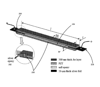
[0020] Fig. 2 illustrates an exemplary schematic diagram of a single two-layer
PZT with shared electrode construction;
[0021] Fig. 3 illustrates an exemplary embodiment in which (a) an experimental
setup for testing a 32 element imaging or a 42 element HIFU linear array, and
(b) a
Cartesian coordinate system with its origin at center of the array;
CA 02849493 2014-03-20
WO 2013/043906 PCT/1JS2012/056393
[0022] Fig. 4 illustrates an exemplary phantom and wires disposed in the
phantom;
[0023] Fig. 5 illustrates an exemplary a graph comparing- the electrical
impedance measurements between (a) a single layer transducer driven in
thickness
mode and (b) a two-layer transducer driven in lateral mode;
[0024] Fig. 6 illustrates some examples of the electrical impedance (a)
amplitude
and (b) phase measurements of the 32-element phased array elements in water;
(1):
lateral mode, (2): thickness mode corresponding to a two-layer array element,
(3):thickness mode corresponding to a single layer transducer;
[0025] Fig. 7 illustrates an exemplary pulse-echo impulse response from the
center element of the 32-element imaging array: (a-b) transmitted pulse
measured and
its corresponding normalized FFT, and (c-d) pulse-echo measurement and the
corresponding normalized FFT of the waveform;
[0026] Fig. 8 illustrates exemplary normalized radiated pressure amplitude
measurements in the XY and YZ planes when the array is focusing: (a-b) at (0,
0, 30)
mm, and (c-d) at (0, 10, 30) mm;
[0027] Fig 9 illustrates a scanned image of the four nylon wires in a phantom;
[0028] Fig. 10 illustrates an exemplary schematic diagram of a 4-layer PZT
transducer with lateral vibration mode;
[0029] Fig. 11 illustrates a frequency spectrum of the 4-layer PZT transducer
with
lateral vibration mode;
[0030] Fig. 12 illustrates an example of a dual-frequency 2-layer PZT
transducer
with lateral vibration mode. (a) construction of an individual element in the
dual
frequency transducer, and (b) fully assembled dual frequency transducer.
[0031] Fig. 13 illustrates an exemplary schematic of the construction of a six
layer
transducer element for a 2-dimensional array, and shows an actual 6 layer
element; and
[0032] Fig. 14 illustrates (a) a sketch of a 8x8 2D array made using six layer
elements; (b) a bottom view of the array showing electrical connectors using
low
temperature solder balls; and (c) a photograph of a 8x8 2D array.
6
Detailed Description
[0033] As discussed above, it is useful to reduce the electrical impedance of
a
phased array and control said electrical impedance to be close to the source
impedance so that said array can be driven without using electrical matching
circuits.
It is also desired to facilitate heat removal from a region of a transducer or
transducer array to keep the same within acceptable operating temperature
limits
during operation, especially at relatively high powers or for relatively long
operating
times. This is especially helpful in situations where the physical
characteristics of the
transducer or array or other components may be adversely affected or altered
or
detuned by an unwanted or unaccounted rise in temperature during operation.
[0034] Some or all of the present inventors and/or applicants have presented
applications for improved transducer device designs and manufacture of the
same.
For example, see, US Pat. Pub. No. 2007/0167764 A1, from US Pat. Appl. No.
11/600,301 and Provisional Appl. No. 60/736,713.
[0035] The present disclosure provides concepts for a design, fabrication and
method of use and driving of a multilayer lateral mode transducer element
(and/or
array) which can be used in diagnostic and HIFU phased array construction. The
present systems and method provide a highly efficient and easy way to reduce
the
large electrical impedance of an array element with small width-to-thickness
ratio
along with temperature reduction for high-power applications.
[0036] As exemplary embodiments, and to validate the lateral coupling
method, we describe below by way of illustration, extension of which will be
apparent
to those skilled in the art, the fabrication and performance of a one-
dimensional
linear 32-element (770 kHz) imaging and a 42-element (1.45 MHz) high intensity
focused ultrasound (HIFU) phased array. The present discussion and examples
showing the benefit of the present lateral mode coupling technique. Both the
arrays
in the present example have been tested by the present inventors and were
driven
without electrical matching circuits. This reduced the amount of time to
fabricate the
arrays as well as the fabrication cost and complexity. Further reduction of
the
electrical impedance can be easily achieved by adding more layers in the
design.
7
CA 2849493 2018-04-20
CA 02849493 2014-03-20
WO 2013/043906 PCT/1JS2012/056393
[0037] In a preferred embodiment, the present multilayer transducer element is
driven in lateral mode of a piezoelectric ceramic plate. To maximize its
performance, we
constructed the arrays from a soft PZT-5 ceramic plate, and took advantage of
its higher
dielectric constant (ET), coupling factor (k31), and electromechanical
constant (d31) than
for the hard PZT ceramic plates (e.g. PZT-4). Table 1 shows the material
properties of a
hard PZT-4 and soft PZT-5 ceramics. Of course, these properties are merely
exemplary
and intended to illustrate the present example, and are not intended to be
limiting or
exhaustive of the possible range of properties that may be employed within the
present
scope.
Parameter
Relative- -dielectric constant 3900
Dielectric. dissipation factor,. tan (.5 0,004 0,018
Curie Temperature .C.C) 250 210
Chew constant, dB (pCIN) 2.5:0 .690
Charge constant, (pCiN) -125 -340
Coupling factor, km 03 0_80
Coupling factor, km 035 -0.46
Density (g/in3) nia 7..95
QukIlity factor, ,..qn -400 46
Table 1.
[0038] Since the PZT-5 has higher k31 and d31 than the PZT-4, it offers higher
transmitting acoustic power output and receiving sensitivity in the lateral
direction. Its
high dielectric constant offers lower electrical impedance so that it requires
less effort to
reduce the electrical impedance than fabricating the transducers with a hard
PZT. The
present results demonstrated that adequate power outputs even for HIFU
purposes
were achieved with the softer material although it is not commonly used for
high power
applications.
[0039] In some aspects, the present lateral mode coupling technique
facilitates
ease of fabrication and reduction of the electrical impedance of the present
devices.
Since we started with large ceramic plates and bonded them under microscope in
the
beginning of the fabrication, we did not experience any misalignment problems.
In some
8
CA 02849493 2014-03-20
WO 2013/043906 PCT/1JS2012/056393
embodiments, we controlled the bonding layer thickness to be equal or less
than about
25 [,tm using 20 ,trri thick silver foils thus decreasing the mechanical
compliance and
coupling losses caused by thick bonding layers. The bonding layer thickness
can be
further reduced using a thinner intermediate conductive foil. Additionally,
since the two
transducer layers always were vibrating in the same manner, either compressing
or
expanding, no delamination problem was observed for two-layer lateral mode
transducers.
[0040] For a multilayer, piezoelectric ceramic array element driven in lateral
mode, it is possible to minimize the electrical impedance of the element by
electrically
connecting multiple transducer layers in parallel and driving them in
unconventional
mechanical vibration mode, the lateral mode.
[0041] Fig. 1 shows an example of three different array element
configurations;
(a) a single layer transducer, (b) a two-layer transducer, and (c) a two-layer
lateral mode
transducer. Specifically, Fig. 1(a) shows a single layer PZT 100 driven in
thickness
mode (indicated by the vibration direction arrows 102). Fig. 1(b) shows a two-
layer PZT
110 driven in thickness mode. Fig. 1(c) shows a two-layer lateral mode PZT
120. The
overall dimensions are the same for the three PZTs. The polarity of the PZT
crystals is
indicated by the poling direction arrows drawn on the faces of the PZT
elements The
transducers shown in Figs. 1 (a-b) will be driven in thickness mode while the
two-layer
lateral mode transducer (Fig. 1(c)) will be used to vibrate in lateral mode.
The elements
of the array, including transducer layers, are poled in the thickness
direction indicated
by the small arrows. For the simplicity of analysis, it is assumed that there
are no
mechanical and electrical losses on the cable and piezoelectric transducer.
The single
layer transducer (Fig. 1(a)) with thickness t, width W, and length / has the
clamped
capacitance Co , given by
[0042]
Co =E0ET Ao /t,
9
CA 02849493 2014-03-20
WO 2013/043906 PCT/1JS2012/056393
where Ao (= I x w) is the electrode area, so is the permittivity of free space
(8.854 x 10⁻¹²
F/m), and ET is the relative clamped dielectric constant of the piezoelectric
ceramic
transducer. The electrical impedance, Zo, is inversely proportional to the
capacitance.
The resonant frequency of the single layer transducer is governed by the
thickness t.
The width w is less than or equal to half the wavelength.
[0043] Fig. 1(b) shows a two-layer transducer driven in thickness mode with a
layer thickness of t/2. The overall dimensions are the same as the single
layer
transducer. With the same transducer thickness t, the resonant frequency would
be
substantially the same as that of the single layer transducer. The inner
electrode
between the transducer layers is connected to ground and the outer electrode
is
connected to the signal line. The total clamped capacitance, CT, and
electrical
impedance, ZT , of the two-layer transducer are
[0044]
Cr = 5051 AT I tr = 2 Eosr (/ x w) / (t/2)
= EOET (2 Ao) / (t/2)
= 4 Co
ZT=1/4 Zo
where the total surface area of the electrodes, AT, doubles and the element
thickness, tT,
decreases by half compared to the single layer transducer. As a result, the
overall
electrical impedance decreases by a factor of four.
[0045] In a two-layer lateral mode transducer (Fig. 1 (c)), the transducer is
driven
at a resonant frequency of the lateral mode instead of the thickness mode.
When an
electric field is applied to the transducer, the two layers simultaneously
vibrate in the
lateral direction with the same phase, both expanding and contracting.
Similarly to the
two-layer transducer shown in Fig. 1(b), the inner electrodes of the layers
are connected
to ground, and the outer electrodes are connected to the signal so the
electrical
connection of the layers is made in parallel. Compared to the single array
element
driven in thickness mode, the fundamental difference in the construction of
the two-layer
lateral mode element is that the thickness of each layer is half the width of
the single
layer element while the width of the layer is the same as the thickness of the
single
CA 02849493 2014-03-20
WO 2013/043906 PCT/1JS2012/056393
element. Therefore, the total electrode area, AL, and layer thickness, tL, of
the two-layer
lateral mode transducer are
[0046]
[0047] The total clamped capacitance, CL, and electrical impedance, a, are
Ct.= toeT 04) = 2 coir (i = 0 / (w12)
4 Co (thvi2,
i W (
e
W
=
[0048] t ,
[0049] where the width-to-thickness ratio, w/t, is always smaller than 1 when
the
V2 center-to-center spacing design rule is used in the phased array
fabrication.
Therefore, the electrical impedance of the two-layer lateral mode transducer
will be
lower than both the single layer and the two-layer transducer driven in
thickness mode.
The resonant frequency of the transducer will be the same or close to that of
the single
layer transducer since they have the same transducer thickness t.
[0050] The present illustrative examples are provided as guides to those
skilled in
the art and are not limiting in their express or implied description of the
embodiments
covered by this disclosure or invention. Other geometries, dimensions and
material
properties and driving signals may also be used in the present context without
loss of
generality or understanding.
11
CA 02849493 2014-03-20
WO 2013/043906 PCT/1JS2012/056393
[0051] Table 2 shows overall comparisons of the electrical impedance between
n-layer transducers driven in thickness and lateral modes in an exemplary
embodiment.
Overall Overall
element tve laver
element element- Cana6tance
coupling mode thicknesi
afen thicknes5
tingle layer I--w
¨ Zot V Co
thickness mode
n-layer n(1 = w)
= 4 Z0
thickne&i mode
n-layer 2 t w
n -71
lateral mode n t :
Table 2.
[0052] The direct comparison shows that the total electrical impedance of an n-
layer lateral mode transducer is (ntlw)2 times smaller than for a single layer
transducer
driven in thickness mode.
[0053] In order to compare the performance thickness and lateral mode
transducers one element with identical dimensions was manufactured with each
method.
The overall dimensions were the same for both the transducers: the thickness t
is 2.4
mm, width w was 0.83 mm, and length /was 20 mm. A single layer thickness of
the two-
layer PZT-5 transducer was 0.4 mm so the resulting width-to-thickness ratio
was 0.33.
The bonding layer with the conductive epoxy and silver foil was approximately
0.05 mm
thick
[0054] We also constructed two one-dimensional linear phased array prototypes
for imaging and therapeutic applications from piezoelectric ceramic plates.
Table 3
shows the design parameters of the two phased arrays.
12
CA 02849493 2014-03-20
WO 2013/043906 PCT/1JS2012/056393
Imaging phased array pbas:ed ainy
Tranaducer material PZT-5 PZT-5
Frequency 750 50 kHz 1.5 ix 0, MHz
Coupling mode Lateral mode Lateiml mode
# of array dementa 32 42
of layers 2 2
Single layer' ilaszlness (mat) 0,4 0.2
Bonding layer (imal) 0,0.25 0.025
.Assembied. atray diluent :4ze Cum 20 0 x 013 (149 x 2.4 (t) 14 0 x 0.43
(*) x
Wiiith-to-rbickosna :ratio (Iwit) 0.33 033
(exchMing the bonding layer)
Table 3.
[0055] Both arrays were fabricated with two-layer lateral mode transducer
elements. The imaging phased array consists of 32 elements with a center
frequency of
750 kHz. It is designed for transcranial imaging applications. Each element is
2.4 mm
thick, 20 mm long and 0.83 mm wide. The 42-element high-intensity focused
ultrasound
(HIFU) phased array was constructed for endocavitary applications, such as for
prostrate tumor ablation. The elements have a center frequency of 1.5 MHz and
dimensions of 14 mm (/) x 0.43 mm (w) x 1.2 mm (t).
[0056] Fig. 2 illustrates placement of a plurality of layers (two shown) of
PZT
elements 200 having conducting (e.g., silver) epoxy termination points 202 and
separated by a soft epoxy medium 204. A pair of conducting (e.g., silver)
electrodes
206, 208 are disposed at opposing ends of the assembly to provide driving
signals
thereto. The PZT elements 200 are arranged in a pair of substantially planar
parallel
plates as shown, sandwiched between thin sheets of highly conducting (e.g.,
gold, Au)
foils 210. The PZTs 200 driven in their lateral mode. The overall thickness of
the two-
layer PZT 200, w, is less than half the wavelength at a given operating
(center) driving
frequency according to some embodiments.
[0057] Stacked (rows) assemblies of such elements adjacent to one another or
packed assemblies (rows and columns, grids, randomly placed elements, radially
placed elements, etc) can be formed to make an overall two or three
dimensional
transducer array assembly. Some embodiments employ electrically driven sets of
transducer elements as described herein so as to form a controllable
ultrasonic field for
use in hyperthermia or focused ultrasound or high-intensity ultrasound therapy
systems.
13
CA 02849493 2014-03-20
WO 2013/043906 PCT/1JS2012/056393
An array of such driven elements is used together, which presents a sound
field in the
ultrasonic range capable of affecting a desired thermal treatment of a patient
suffering
from a disease.
[0058] Diagnostic applications of the present PZT systems also exist. For
example, a system can include an array of 32-elements or more for use as an
imaging
array. Yet other applications include a plurality (e.g., dozens or hundreds)
of driven
elements for use in an endocavitary high intensity focused ultrasound (HIFU)
array,
constructed using the lateral mode coupling method described above shows a
schematic diagram of a single two-layer lateral mode transducer element
according to
an embodiment.
[0059] The basic fabrication process is the same for the imaging and HIFU
phased arrays. For example, in the first step of the imaging phased array
fabrication,
two 70 mm x 20 mm PZT-5 plates (e.g., TRS610HD, TRS Ceramics, State College,
PA,
USA) with a thickness of 0.2 mm were bonded with soft epoxy (301, Epoxy
Technology , Billerica, MA, USA). Before bonding the two PZT-5 transducers,
small
pieces of 20 mm thick silver foils (e.g., GoodFellow, Oakdale, PA, USA) are
sandwiched
between the two transducers on each side and electrically connected to the
inner
electrodes of the two transducers using silver epoxy (e.g., GPC 251,
CreativeMaterials,
Tyngsboro, MA, USA). In the present example, relatively small sections of the
foils
between the transducers were used to make the electrical connection to reduce
or
eliminate problems caused by adding the silver foils, such as mechanical
compliance
changes. The foils are also used to bridge the electrical connection between
the
elements and connector. In the bonding processes, a mechanical clamp was used
to
compress the two transducers to minimize excessive bonding material and to
control
the overall bonding layer thickness to be the same as that of the silver foil.
In one
embodiment, approximately 2 mm of silver foil is sandwiched between the
transducers
with an additional 1 mm left exposed for wire connection.
[0060] The inner electrode may be connected to the signal line (+), and
another
set of electrodes on the top and bottom to ground (-). The conductive epoxy
(e.g. silver
epoxy) may be applied to only one of the silver foils and connected to the top
and
bottom electrodes for the ground connection. Then, as shown in the figure, the
silver foil
14
CA 02849493 2014-03-20
WO 2013/043906 PCT/1JS2012/056393
connected to the ground is disconnected from the inner electrodes by dicing
through the
bonded transducers deep enough to cut the sandwiched silver foil at 1 mm from
the
transducer edge. The kerf may be filled with the soft epoxy and 300 nm thick
gold was
evaporated onto the surface of the transducer. Individual elements are diced
to 2.4 mm
long from the fabricated 70 mm long, 20 mm wide, two-layer PZT-5 plates.
Custom-
designed, 1 m long coaxial cables (e.g., Precision Interconnect, Berwyn, PA,
USA) may
be used to make electrical connection between the element and a ZIF connector
(e.g.,
ITT Cannon, Shakopee, MN, USA).
[0061] Before the final assembly process, the silver foils are coated with
approximately 20 mm thick Parylene and thin layer of the soft epoxy to prevent
from
short circuits between adjacent array elements. Then, the individual elements
may be
bonded using silicone to minimize mechanical coupling between the elements.
After
finishing the assembly, the overall center-to-center spacing was measured
under a
microscope to be equal to or smaller than half the wavelength in water. A 5 cm
thick
backing material (e.g., PZT-4 powder/soft epoxy = 2:1) is applied on the
backside of the
phased array. A 10 mm thick Parylene layer may be coated on the array surface
to
protect the elements from corrosion and mechanical damage.
[0062] Similarly, transducer elements of a HIFU array can be fabricated to be,
e.g., 14 mm (I) x 1.2 mm (t) x 0.43 mm (w) using two 0.20 mm thick PZT-5
ceramics
(e.g., TRS610HD, TRS Ceramics, State College, PA, USA). The overall
fabrication
process can be the same as for the imaging array. Instead of using long
coaxial cables,
the elements are mounted on a printed circuit board (PCB) and individual
electrical
connection from the silver foils to the PCB board are made using 50 mm thick
copper
wires (e.g., California Fine Wire, Grover Beach, CA, USA). No backing material
is
required for the array in some embodiments. These arrays and others can be
constructed using the present lateral mode coupling method.
[0063] To validate the performance of the present lateral mode coupling
method,
the electrical impedance of the two-layer lateral mode elements can be
measured using
a network analyzer. A simple electrical impedance comparison between a single
thickness mode and two-layer lateral mode transducers can be conducted by
evaluating
CA 02849493 2014-03-20
WO 2013/043906 PCT/1JS2012/056393
the measurement in air. Overall electrical impedance measurements for the
imaging
and HIFU arrays can be performed in degassed and deionized water.
[0064] Fig. 3(a) shows the overall experimental setup 300 for the measurement
of the pressure field radiated from the arrays 310. A tank holds the
experiment and is
lined with 1 cm thick rubber to minimize any acoustic reflections from the
tank walls, and
filled with degassed, deionized water (Resistivity > 16 MQ-cm), with dissolved
oxygen
level maintained below 1 ppm. The Cartesian coordinate system 320 used in the
study
is shown in Fig. 3(b). The origin of the coordinate system 320 is located at
the center of
the array 310 as shown, and the acoustic axis is parallel to the z axis. The
ultrasound
pressure fields radiating from the imaging and HIFU arrays are measured with a
40 mm
long, 125 mm diameter planar fiber-optic hydrophone (e.g., Precision
Acoustics,
Dorchester, UK). A hydrophone 312 is moved with a 3-D scanning system 314
(e.g.,
Velmax Inc, Broomfield, NY, USA). A 42- element HIFU array 310 is then driven
by an
amplifier system 340 with a plurality (e.g., hundreds, dozens) of channels as
needed. Of
course, the present description is only exemplary, and those skilled in the
art appreciate
other ways of doing the same or substantially same or equivalent steps using
various
devices suited for the purpose.
[0065] A tone burst signal (e.g., PRF = 330 kHz, duty cycle = 1%) is used to
drive
each element of array 310. An electrical power of a 1 W/channel can be used to
measure the radiated fields from the array in an example. The electrical-to-
acoustic
power conversion efficiency and maximum surface acoustic power of a single
element
of the HIFU phased array are measured using a scanning laser vibronneter
(e.g., PSV-
400-M2-20 20MHz, Polytec, Tustin, CA, USA).
[0066] For single element experiments of the imaging array a pulser/receiver
(e.g., Panametric 5072PR, Olympus, Waltham, MA) is used to transmit and
receive the
RF-signal. In these cases the received waveform is recorded using a digital
oscilloscope.
A commercial 32-channel imaging scanner (e.g., OPEN system, Lecoeur
Electronique,
Cheulles, France) is used in the experiments with the whole array. It is
controlled via
USB with custom-built C++ software running on a desktop computer. The OPEN
pulser/receiver system excites the array with a 50 Vpeak and 12.5 ns long
pulse, and
received echo signals. The received echo signals is filtered using a zero-
phase
16
CA 02849493 2014-03-20
WO 2013/043906 PCT/1JS2012/056393
bandpass digital filter in MATLAB (e.g., Mathworks, Natick, MA, USA). Then, a
Hilbert
transform is performed to obtain the envelope of the signals. The images are
acquired
with a 300 serial scanning of the transmit and receive focus at half-degree
increments
in elevation angle. The beam is focused 60 mm from the transducer surface.
Each scan
line has a delay of 50 ps and 65 dB gain applied on all channels. The
feasibility of
imaging can be for example determined using a water phantom 420 with four 300
pm
thick Nylon wires, as shown in Fig. 4. The first three wires are separated
from each
other by approximately 5 mm axially, 7 mm in elevation (8.6 mm on the
diagonal). The
fourth wire 420 is 10 mm axially, 13 mm elevation away from the third wire.
[0067] Again, none of the present detailed examples shall be considered
limiting
of the present invention, but rather as a particular example to aid the
understanding of
those skilled in the art.
[0068] Fig. 5 illustrates a comparison of the electrical impedance
measurements
of a single layer transducer driven in thickness mode in an exemplary
embodiment (Fig.
5(a)) and a two-layer lateral mode transducer (Fig. 5(b)). The impedance
amplitude 500
in air at the maximum phase for the single layer thickness mode transducer was
approximately 3000 Q at 840 kHz. The two-layer lateral mode transducer had an
impedance amplitude of 73.3 1.2 Q at 770 kHz in air, which is 41 times
smaller than
that of the single layer with the same dimensions. This demonstrates the
electrical
impedance reduction without using a traditional method, such as employing an
electrical
matching circuit. In addition, the large electrical impedance of the small
array element
can be made to be close to the source impedance by controlling the number of
layers
and their thickness.
[0069] Fig. 6 shows an example of the electrical impedance plots of a fully
assembled 32-element two-layer lateral phased array, measured in deionized
water.
The plots show the resonant frequencies at 770 kHz, 1.5 MHz and 3.4 MHz,
respectively. The strong modes are shown at 770 kHz for the lateral mode of
the
element (600) and at 3.4 MHz for the thickness mode of the single layer
transducer
(610). Here, the thickness mode of the two-layer element at 1.5 MHz, was not
as strong
as the other two modes. The electrical impedance amplitude at 770 kHz is 58 3
Q at
the maximum phase angle of -1.2 .
17
CA 02849493 2014-03-20
WO 2013/043906 PCT/1JS2012/056393
[0070] Fig. 7 shows a typical pulse-echo impulse response from the center
element of the 32- element imaging phased array, reflected off a 5 cm thick
acrylic plate
from the array. Fig. 7(a) and (b) show a transmitted pulse measurement and its
corresponding normalized FFT. In the present embodiment, there was no matching
circuit used to compensate electrical impedance mismatch. The -6 dB and -40 dB
pulse
lengths of the waveform are 1.6 ps and 3 ps, respectively, which correspond to
approximately 1.2 and 2.3 cycles at 770 kHz. The corresponding normalized FFT
(Fig.
7(d)) shows that the array has a center frequency of 770 kHz with -6 dB
bandwidth of
approximately 52%, measured at lower and upper frequencies of 612 kHz and 1.02
MHz. It should be appreciated that an electrical matching circuit may be
employed in
some applications, as deemed appropriate, but that the present designs and
techniques
can alleviate or eliminate the need for such circuits in some or many or all
cases.
[0071] Fig. 8 illustrates radiated pressure amplitude field measurements in
the
XY and YZ planes when the array was focusing at (0, 0, 30) mm and (0, 10, 30)
mm.
The field measurement shows a good steering capability of the 1D linear array.
[0072] Fig. 9 shows a scanned image of a bath containing four 300 mm thick
Nylon wires as described earlier. The first three wires were shown to be
approximately 5
mm axially, 7 mm in elevation apart each other, and the fourth wire 900 was
seen at 10
mm axially, 13 mm elevation away from the third wire 910.
[0073] Similar laterally coupled transducers can be used to increase the
bandwidth of the elements by making the transducer plates of different lengths
such that
they resonate at different frequencies such that a combined wideband operation
is
achieved.
[0074] An example of such a 4-layer PZT transducer with lateral vibration mode
element is shown in Fig. 10, with its associated frequency spectrum in Fig.
11. In some
aspects, 1-, 1.5- or 2-dimensional arrays can be formed from such elements
according
to the present teachings.
[0075] Dual-frequency or multi-frequency arrays 1200 can be formed by making
the transducer elements from plates of two different lengths (e.g., 1202,
1204) so that
they resonate at the desired frequencies corresponding to the lengths (or in
the context
18
CA 02849493 2014-03-20
WO 2013/043906 PCT/1JS2012/056393
of an array to the respective thicknesses of the transducer array elements).
This is
depicted for a pair of different sized elements in Fig. 12(a).
[0076] Fig. 12(b) shows a fully assembled dual frequency transducer array
1210.
In other embodiments, this can be extended to any number of frequencies and
all
transducer and array configurations and geometries. Stacking, packing and
distributing
the array elements in the face or body of the transducer array is also
possible.
[0077] The same method for making the above systems can, again, be extended
to 1.5 or 2 dimensional arrays as shown in Figs. 13 and 14, respectively.
[0078] Fig. 14(a) illustrates a perspective view of an exemplary 2D array
showing
its front (transducer/emission side) face having a plurality of rows and
columns arranged
thereon. Acoustic energy radiates outwardly from each driven element of the
transducer generally normally away from the active face of the transducer.
Fig. 14(b)
illustrates the 20 array from its front (transducer/emitter) side. For 2D
arrays 1400 the
transducer element widths can be selected such that the complete multilayer
element
will be more or less square. Therefore thinner and a larger number of plates
can be
used to reach the desired impedance.
[0079] For an imaging array, its narrow bandwidth could be improved by adding
acoustic impedance matching layers on the array's front surface or using a
different
backing material. The electrical-to-acoustic power conversion efficiency of
the HIFU
array can be easily increased using more transducer layers in the element
design. This
transducer structure is fully scalable and therefore it is expected that even
high
frequency imaging arrays up to and beyond 100MHz can be constructed.
[0080] What is claimed is:
19