Note: Descriptions are shown in the official language in which they were submitted.
CA 02849533 2015-10-08
4
,
UNIVERSAL PHASE DIMMING MODULE
FIELD OF THE INVENTION
The present invention is directed to a lighting control system that provides
dimming and
that operates over a wide input voltage range.
BACKGROUND
Dimmer circuits and dimmer cabinet assemblies currently offered in the market
are
typically specific to the voltage of the power circuit since many of the main
components of the
dimmer circuit are designed to operate at a specific voltage or a very narrow
voltage range. As a
result manufacturers, distributors, and retailers need to produce and stock
multiple versions of
dimmer circuits and dimmer cabinet assemblies. They also need to make sure
that the correct
dimmer circuit or dimmer cabinet assembly is provided to their customer. It
would be simpler if
a single dimmer circuit or a single dimmer cabinet assembly could operate over
a wider voltage
range because it would minimize the number of different dimmer circuits and
dimmer cabinet
assemblies required and would reduce the possibility of filling an order with
the incorrect
product.
1
CA 02849533 2014-04-22
SUMMARY
The present invention is directed to a lighting control system and its
components
configured to operate across a wide range of input voltages or across multiple
ranges of input
voltages.
One aspect of the invention is directed to a dimmer circuit that provides
reverse phase cut
mode dimming, forward phase cut mode dimming, and hybrid phase cut mode
dimming. The
dimmer circuit may include transition time control, over current protection,
and inductive load
sensing. Thermal protection for the module may be provided through a
combination of physical
components and firmware.
Another aspect of the invention is a universal load control module. The
universal load
control module may combine functional control blocks, such as a dimmer
circuit, a control
interface and/or a communications interface, along with a microcontroller and
a power supply
that can operate across a wide voltage range.
In yet another aspect of the invention, a cabinet houses multiple universal
load control
modules. The cabinet may include a cabinet control module, which configures
and controls the
modules, as well as provides an external interface. The cabinet may also
include features to
assist with thermal protection, such as a thermal shelf, spaced apart branch
circuit breakers and
an optional cooling device.
2
CA 02849533 2014-04-22
BRIEF DESCRIPTION OF THE DRAWINGS
These and other features, aspects, and advantages of the present disclosure
are better
understood when the following Detailed Description is read with reference to
the accompanying
drawings, where:
Fig. 1 is a block diagram of an exemplary universal phase dimming module.
Fig. 2 is a block diagram of an exemplary universal power supply.
Fig. 3 is a circuit diagram of an exemplary zero cross detection circuit.
Fig. 4 illustrates an output of the exemplary zero cross detection circuit of
Fig. 3.
Fig. 5 is a circuit diagram of an exemplary dimmer circuit.
Fig. 6 illustrates reverse phase cut mode dimming for an exemplary dimmer.
Fig. 7 illustrates forward phase cut mode dimming for an exemplary dimmer.
Fig. 8 is a circuit diagram of an exemplary dimmer with temperature-based slew
rate
control.
Fig. 9 is a circuit diagram of an exemplary dimmer circuit with multistage
transitional
control.
Fig. 10 is a block diagram of an exemplary current sense device.
Fig. 11 is a circuit diagram of an exemplary dimmer circuit with inductive
load sensing.
Fig. 12 illustrates an output of the exemplary inductive load sensing circuit
of Fig. 11.
Fig. 13 illustrates hybrid phase cut mode dimming for an exemplary dimmer.
Fig. 14 is a block diagram of an exemplary universal load control module.
Fig. 15 is a front view of an exemplary load control cabinet without its front
panel.
Fig. 16 is a front view of a front panel of an exemplary load control cabinet.
3
CA 02849533 2014-04-22
Fig. 17 illustrates the arrangement of branch circuit breakers in an exemplary
load control
cabinet.
Fig. 18 illustrates the placement of a main circuit breaker in an exemplary
load control
cabinet.
Fig. 19 illustrates a thermal shelf in an exemplary load control cabinet.
DETAILED DESCRIPTION
The present invention is directed to a lighting control system and its
components, and in
particular to a dimmer circuit, a load control module that may include the
dimmer circuit, and a
load control cabinet that may include the module. The system and its
components are configured
to operate across a wide range of input voltages or across multiple ranges of
input voltages. The
system may provide multiple dimmers and include thermal protection. A load
control module
may include one or more dimmers and/or a control or communication interface. A
cabinet
assembly may include multiple load control modules controlled by a cabinet
control module.
Alternatively, a single load control module may be configured to operate in a
stand-alone mode.
The system and/or its components may be referred to as "universal" or "multi-
volt" since
they can operate over a wide range of input voltages or over multiple ranges
of input voltages.
Typically, the system does not require user intervention to configure the
system or its
components to any particular input voltage. Instead, the components of the
system automatically
adjust to the input voltage. In an exemplary lighting control system, the
input voltage may be
120/230/277Vac, 50/60 Hz. Other systems may operate with different input
voltages, including
voltages up to at least 347Vac.
4
CA 02849533 2014-04-22
One aspect of the invention is a dimmer circuit. The dimmer circuit may
include
circuitry to support reverse phase cut mode dimming, forward phase cut mode
dimming, and
hybrid phase cut mode dimming. The dimmer module may also include ON/OFF and
slew rate
control, wave shaping, transition time control, over current protection, and
inductive load
sensing. Thermal protection for the module may be provided through a
combination of physical
components and firmware.
Another aspect of the invention is a universal load control module. The
universal load
control module may combine functional control blocks, such as a dimmer, 0-10V
control, a
DALI interface, etc. in a single module. The universal load control module may
operate
independently or may be controlled with other universal load control modules
by a cabinet
control module.
In yet another aspect of the invention, a cabinet houses multiple universal
load control
modules. The cabinet may include a cabinet control module, which configures
and controls the
modules, as well as provides an external interface.
Universal Phase Dimming Module
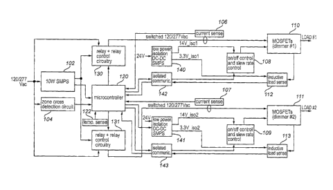
Fig. 1 is a block diagram illustrating an exemplary universal phase dimming
module that
operates over multiple voltage ranges. The universal phase dimming module
includes a power
supply 102, a zero cross detection circuit 104, a microcontroller 120,
optional relay and relay
control circuitry 130, 131, power switching devices 110, 111, ON/OFF and slew
rate control
circuitry 108, 109, inductive load sense circuitry 112, 113, current sense
circuitry 106, 107, and
temperature sense circuitry 122. Although Fig. 1 illustrates an embodiment
that supports two
dimmers (dimmer #1, dimmer #2) connected to two loads (LOAD #1, LOAD #2),
other
CA 02849533 2014-04-22
embodiments may support a different number of dimmers and loads. The dimmer
circuit may be
configured for forward phase cut (FPC), reverse phase cut (RPC) and hybrid
phase cut (HPC)
operating modes.
A relay and relay control circuitry 130, 131 may be used in a dimming system
that uses a
three-wire ballast. An electro-mechanical relay may be placed in series with
the dimmer output
to provide air gap isolation when the dimmer is in the OFF state. In this
implementation, the
inputs to the three-wire ballast include the output of the relay, the phase
control signal output by
the dimmer, and neutral. In other applications, the relay and relay control
circuitry may not be
needed.
Fig. 1 illustrates a signal from the microcontroller to the low power
isolation DC-DC
switched mode power supply 141. This signal may be an enable signal or it may
be a PWM
(pulse width modulation) control signal output by the microprocessor. The
signal controls the
low power isolation DC-DC switched mode power supply 141 so that it powers
down the
dimmer circuitry when the dimmer is OFF. A similar signal may be provided to
the low power
isolation block 140 (not shown). In applications that are not efficiency
sensitive in the OFF
state, the signal from the microcontroller may not be needed.
The microcontroller 120 outputs the PWM control signal to the isolated
communication
block 142, 143. The isolated communication block includes an isolated coupler,
such as an
optocoupler, digital isolator, or a magnetic coupler. The microcontroller
varies the duty cycle of
the PWM control signal to control the phase control signal output by the
dimmer.
The microcontroller may include computer-readable memory or it may access
external
computer-readable memory that includes computer-executable instructions for
lighting control,
including dimming. The instructions may be related to lighting control, such
as dimmer curves,
6
CA 02849533 2014-04-22
rooms and zones, time scheduling, or may be related to thermal control. The
microcontroller
may also receive one or more inputs that direct the microcontroller to control
the dimmer based
on the received input. The inputs may come directly from a user or through an
intervening
interface, such as that provided by a cabinet control module.
Power Supply
The dimmer circuit includes a switched mode power supply (SMPS) which is
compatible
with a wide input voltage range, e.g., 120/277 Vac, 50/60 Hz. Fig. 2
illustrates one
implementation of a power supply 102 that provides 24V and 3.3V DC outputs to
the remainder
of the control and dimmer circuit. The power supply automatically detects the
input voltage and
adjusts its operations as needed to provide a regulated output voltage without
requiring user
intervention. Other power supplies may be used so long as they have the
ability to work across
multiple voltage ranges or a wide voltage range, preferably without requiring
user intervention.
Zero Cross Detection Circuit
The zero cross detection circuit 104 is compatible with a wide input voltage
operating
range. An exemplary zero cross detection circuit is shown in Fig. 3 and
utilizes high value input
resistors, an efficient R-C trigger circuit, and a transistor to drive an
isolating optocoupler, which
provides isolation for an input to the microcontroller. The output of the zero
cross detection
circuit ("out" in Fig. 2) is provided to the input of the microcontroller.
The exemplary zero cross detection circuit differs from conventional designs
which use
simple current limiting resistors to drop the input voltage into the isolating
optocoupler.
Conventional designs balance power loss and heat in the resistors with the
input current
requirements for the optocoupler, and this balancing exercise precludes its
use over a wide input
voltage range, since the resistors which provide enough current at lower
voltages dissipate too
7
=
CA 02849533 2014-04-22
much power for long-term reliability at the higher voltages. Other
conventional designs may
include comparators, op amps, 555 timers or inexpensive microcontrollers that
all require a low
power universal input power supply to provide a regulated low voltage
signal/power to digital
and/or analog electronics.
In the exemplary zero cross detection circuit of Fig. 3, the universal input
waveform is
sampled with the voltage divider network (R1, R2, R3), energy is stored in
capacitor (C1) and
the stored energy is released through the optocoupler and current limiting
resistor (R4) when the
sampled signal is less than approximately 14.3 V on the base of the transistor
(Q1). The output
pulse on the isolated side of the optocoupler corresponds to the zero crossing
of the sampled AC
input voltage. This simplified comparator functionality doesn't require a
constant or regulated
power supply. Therefore, the reliability and expected lifetime of the circuit
is significantly
improved while still providing a low cost solution. The component values
illustrated in Fig. 3
are exemplary. Other values, as well as other zero cross detection circuits
may be used.
Fig. 4 shows the output pulses corresponding to the zero cross points on the
input power-
line AC voltage (hot to neutral). The signals would be similar for other
inputs (e.g., 120 Vac -
277Vac) received on the universal input. The microcontroller uses the zero-
crossing information
from the zero cross detection circuit to synchronize its internal timer with
the 60/50 Hz input
power. This allows the microcontroller to provide a PWM control signal
synchronized with the
input power, which results in smooth and flicker¨free dimming performance.
Although a zero cross detection circuited is needed for a phase dimmer,
circuit designs
other than that illustrated in Fig. 2 may be used.
8
CA 02849533 2014-04-22
Power Switching Devices
Conventional dimmers may use power switching devices, thyristors such as
Silicon
Controlled Rectifiers (SCRs), and/or Triacs. These devices require a "latching
current"
(typically greater than several milliamps) to allow the devices to continue
conducting once
triggered. The requirement for a latching current makes these devices
inappropriate for use with
modern efficient lighting loads, such as LEDs, which not only draw less
current, but also may
not draw it consistently enough to keep a thyristor latched.
Additionally, thyristor-based dimmer designs require series inductive
filtering to reduce
the EMI emitted from the dimmer, as well as the acoustic noise that the
powerline switching can
induce in the lamps (commonly referred to as "filament sing"). These types of
filters are both
load and voltage dependent, and a filter which is designed for a 277 V circuit
will not have
acceptable performance for smaller loads at 120 V.
The dimmer circuit uses power switching devices (110, 111 of Fig. 1; Ul, U2 of
Fig. 5),
such as IGBTs or MOSFETs, which do not require either a minimum latching
current or a series
inductive filter, to allow the dimmer circuit to operate over a wide range of
input voltages.
Transition Control, Including ON/OFF and Slew Rate Control
The dimmer circuit also includes circuitry to control the ON/OFF time and the
slew rate.
By controlling the slew rate, the dimmer circuit provides a constant fall rate
di/dt for reverse
phase cut dimming (See Fig. 6) and constant rise rate di/dt for forward phase
cut dimming (See
Fig. 7). By controlling the slew rate, the voltages across the dimmer load
exhibit a similar rate of
voltage change (dv/dt). Slew rate control is important for compliance with the
FCC standard for
radiated/emitted and conductive noise. A dimmer with slew rate control emits
significantly
9
CA 02849533 2014-04-22
fewer harmonics than a dimmer without slew rate control. Slew rate control
also eliminates the
buzzing noise associated with dimming incandescent bulbs with forward phase
cut dimmers.
Conventional forward phase cut dimmers that use Triacs and SCRs require a
relatively
large inductor to provide series inductive filtering to control the slew rate
of the dimmer. In
these designs the slew rate is variable based on the load current, so the
published slew rate is
only applicable for specific load test conditions. In the present dimmer
circuit, the slew rate is
independent of the load current. The negative feedback components (C1, R7, C2,
R8) provide
feedback to gates of the MOSFETs (U1, U2) in order to regulate the transition
time from an ON
to OFF state and vice versa. The negative feedback components are not needed
in
implementations that use IGBT power switches since negative feedback is
inherent in IGBT
power switches. However, the external current limiting programming resistors
on the gates of
the IGBTs are necessary to control the rise/fall rates.
The dimmer circuit may include circuitry for ON/OFF and slew rate control. The
ON/OFF and slew rate control may be combined into a single functional block,
as shown by 108
and 109 of Fig. 1.
Fig. 5 illustrates an exemplary ON/OFF and slew rate control circuit 504, an
exemplary
wave shaping circuit 502, and an exemplary dimmer output circuit 501. The
ON/OFF and slew
rate control circuit 504 may include transistors (Q1, Ml, M2), as well as
other components. The
microcontroller controls the transistors by providing a PWM control signal to
the circuit. In one
implementation, the PWM control signal is fed to the circuit through an
optocoupler or a digital
coupler.
The power switching devices, such as the MOSFETs (U1, U2), operate in the
linear mode
(or resistive or active region) during the transition from the OFF to ON
states and the ON to OFF
CA 02849533 2014-04-22
states. The ON/OFF and slew rate control circuit is one option for decreasing
the heat
dissipation on the power switching devices during the transition from the OFF
to ON states and
the ON to OFF states. The ON/OFF and slew rate control circuit reduces heat
dissipation by
reducing the transition time, or slew rate, between the ON/OFF states. For
example, the power
switching devices dissipate more heat when the transition time is 350us, than
when the transition
time is 165us. Additional options may also be used to dissipate heat,
including a heat sink.
When the dimmer provides reverse phase cut mode dimming, the ON/OFF and slew
rate
control circuitry controls the transition time (slew rate) at the falling edge
of the phase control
signal, as shown in Fig. 6. When the dimmer provides forward phase cut mode
dimming, the
ON/OFF and slew rate control circuitry controls the transition time (slew
rate) at the rising edge
of the phase control signal, as shown in Fig. 7. The phase control signal
corresponds to the
PWM control signal from the microcontroller in that the on time of the
waveform corresponds to
the pulse width of the PWM control signal.
The wave shaping circuit 502 of Fig. 5 is used in reverse phase cut and hybrid
phase cut
modes to prevent possible oscillations or stability issues with the power
switching devices. The
wave shaping circuit provides a hard turn-off after a predetermined time based
on the time
constant of the circuit. In one implementation, the circuit is tuned so that
the predetermined time
is 165 us at 50% duty cycle.
During the ON/OFF or OFF/ON transition the power switching devices operate in
the
active/linear region and dissipate significant amounts of power resulting in
higher operating
temperatures. Due to the negative temperature coefficients of D2 and Q2
(approximately -
2mV/C) in the wave shaping circuit 502, there is a variable negative time
constant that is linearly
proportional with the ambient temperature inside the dimmer. As a result,
there is nominal turn-
11
CA 02849533 2014-04-22
off control of the dimmer at 25C ambient temperature and reduced turn-off
control at higher
operating temperatures, which provides a first level of thermal protection for
the dimmer.
Thermal Protection
The dimmer circuit may monitor temperature and use the temperature to adjust
the
operation of the dimmer to provide thermal protection other than the nominal
turn-off control
described in the preceding paragraph. Fig. 8 illustrates one thermal
protection option. In Fig. 8
the resistors R2, R3 of Fig. 5 are replaced with thermistors (NTCs) so that
the slew rate is
adjusted based on ambient temperature. In reverse phase cut mode, the wave
shaping circuit 802
automatically reduces transition time (automatic fold-back) with higher
ambient temperature so
that the dimmer is turned off faster at higher temperatures. This reduces the
power dissipation
across the dimmer and provides dynamic thermal protection. The actuation time
of Q2 is
controlled by D2 which is dependent on the ambient temperature. In one
embodiment the circuit
operates as follows: at 25C the wave shaping circuit actuates at 165 us, at
50C it actuates at 125
us, at 75C at 100 us, etc. When Q2 actuates, the gate voltage is pulled to
ground and the power
switching devices (U1, U2 in Fig. 8, 110, 111 in Fig 1) turn OFF and exit the
resistive or active
or linear mode of operation.
Fig. 9 illustrates another alternative to Fig. 5. Instead of the
microcontroller controlling
the ON/OFF and slew rate circuitry shown in Fig. 5 via the PWM control signal,
the
microcontroller selects a specific transition circuit 902, 904 or 906 by
providing dual PWM
control signals to the selected circuit. The different transition circuits
provide different transition
times. One advantage of the multistage transition control shown in Fig. 9 is
that it provides
multiple transition time options, instead of a single transition time (e.g.,
165us at 50% duty
cycle), as provided by the single stage of Fig. 5. Fig. 9 illustrates three
transition circuits, 902,
12
= CA 02849533 2014-04-22
904, 906. One of the transition circuits 902 provides a long transition time,
e.g., 350 us, a second
transition circuit 904 provides a medium transition time, e.g., 165 us, and a
third transition circuit
906 provides a short transition time, e.g., <10 us. The programming resistors
(R1, R2, R3)
determine the transition timing for each transition circuit. A larger value
will set a longer or
slower transition rate, whereas a smaller resistor value will provide a faster
or shorter transition
rate. The microcontroller selects transition circuit 902 using Trans LON and
Trans l_OFF,
selects transition circuit 904 using Trans2 ON and Trans2_OFF, and selects
transition circuit
906 using Trans3_0N and Trans3_OFF. For example, when transition circuit 902
is selected,
the on time of the phase control signal is based on the pulse width of the PWM
control signal
applied to Trans 1_0N and the off time of the phase control signal is based on
the pulse width of
the PWM control signal applied to Trans l_OFF.
In one embodiment, the microcontroller selects the transition time based on
temperature,
such as the ambient temperature or MOSFET temperature. The microcontroller
selects the long
transition time circuit 902 when the dimmer is operating at safe/normal
temperatures, selects the
medium transition time circuit 904 when the dimmer is running hot, and selects
the short
transition time circuit 906 when the ambient temperature is near the safe
operating limits and/or
the dimmer is overloaded causing high temperatures on the power switches. The
short transition
time circuit 906 provides a minimum transition time so that the power
switching devices operate
in the linear region for a shorter time and thus dissipate less power.
In one implementation the microcontroller compares the temperature to stored
values or
thresholds. If the temperature is below a first threshold, then the
microcontroller selects the long
transition time. If the temperature is between the first threshold and a
second threshold, then the
13
CA 02849533 2014-04-22
microcontroller selects the medium transition time and if the temperature is
above the second
threshold, then it selects the short transition time.
In an alternative implementation, only one transition circuit with an
adjustable resistor.
In this implementation, the programming resistor (e.g,. RI) is replaced by an
adjustable resistor
and the different values provide different transition times. For example, the
adjustable resistor
could be a programmable digital potentiometer with for example 64 or 128 taps.
Each tap selects
a different internal resistor that provides a different transition rates
(64/128/256/etc.).
Alternatively, this could also be accomplished in the analog domain with J-
FET, MOSFET or
BJT operating in the active/resistive/linear region to have an infinite number
of programmable
resistor values. An op amp/comparator circuit configuration may be used for
setting the
programmable resistor values.
Although not shown in Fig. 9, a wave shaping circuit such as that shown in
Fig. 5, may
also be included to support reverse phase cut mode or hybrid phase cut mode
dimming.
Additional or alternative thermal protection may be provided by the
microcontroller 120
by controlling the phase angle or duty cycle of the PWM control signal based
on temperature.
The microcontroller may obtain temperature information from a temperature
sensor 122 of Fig.
1. The temperature sensor may be a thermistor, temperature sensor, diode, an
internal
temperature sensor on the microcontroller, or any other suitable sensor. In
one example, the
ADC value of the measured temperature is an input to P/PI/PID
(proportional/proportional-
integral/proportional-integral-derivative) microcontroller, which may be
implemented in
firmware on the microcontroller.
If the ambient temperature in the proximity of power switching devices (or
direct
temperature measurement on the power devices' packaging) exceeds a temperature
threshold for
14
CA 02849533 2014-04-22
the power switching devices and the phase angle exceeds a phase angle
threshold, e.g., greater
than 55%, then the microcontroller increases the duty cycle of the PWM control
signal to
decrease the power dissipation on the power switching devices and therefore
slow the
temperature rise of the die junction inside the silicon power switching
devices
(MOSFETs/IGBTs/etc). If the temperature is still above the temperature
threshold when power
switching devices are at 100% duty cycle, then the microcontroller will
control the PWM control
signal to provide a 0% duty cycle to turn off the dimmer to protect it from an
over-temperature
condition. If the temperature exceeds the temperature threshold and the phase
angle is less than
the phase angle threshold, e.g. less than 55%, then the microcontroller
decreases the duty cycle
of the PWM control signal to decrease the power dissipation on the MOSFETs and
therefore
lowers the die junction temperature within the Safe Operating Area (SOA as
specified in the
datasheet from power switching device manufacturer). The P/PI/PID control
algorithm stabilizes
the dimmer response and eliminates rapid dimming control fluctuations.
Over Current Protection
The dimmer module of Fig. 1 may include current sense devices 106, 107, such
as a
current sense transformer, Hall affect sensor, current sense resistor, etc.
Fig. 10 illustrates an
exemplary Hall affect sensor.
The microcontroller receives an output signal from the current sense device
via an ADC
input, calculates the rms value and measures the peak value, and ensures that
the maximum rms
and peak ratings of the dimmer are not exceeded. The microcontroller
determines if the duty
cycle of the PWM control signal needs to be reduced, or if the dimmer needs to
be turned off in
order to protect the power switching devices from failure.
CA 02849533 2014-04-22
Another purpose of the current sense device is to detect if any of the power
switching
devices 110, 111 of Fig. 1 failed open or in a shorted condition. The
microcontroller sets the
PWM control signal output to maximum if one device fails short. This prevents
possible large
loading unbalance in a single or three phase system. It also disables dimming,
which provides an
indication to the user of the failure.
Inductive Load Protection
In one implementation, the default dimmer operating mode is reverse phase cut
dimming.
This operating mode avoids the inrush current and resulting buzzing noise when
incandescent
lamps are dimmed with a standard forward phase cut dimmer. One disadvantage of
reverse
phase cut dimming is that the current through the load is disrupted abruptly.
This is not an issue
for resistive (current in phase with voltage, e. g., incandescent/tungsten
bulbs) and capacitive
(current leading voltage) loads. However, for inductive loads (current lagging
voltage) this
condition could damage the dimmer. Disrupted current flow though the inductive
load could
create a large flyback voltage and the dimmer circuit will fail if the peak
flyback voltage exceeds
the maximum voltage withstand rating of the power switching devices.
The dimmer circuit may also include an inductive sense circuit, as shown in
Fig. 1, 112,
113, to detect the flyback voltage. An exemplary inductive sense circuit 1102
is further
illustrated by Fig. 11. The circuit includes a comparator, sampling circuit,
and reference voltage
and generates an output signal that is transmitted through an isolated
coupling device to the
microcontroller, which notifies the microcontroller that the flyback voltage
is present with a peak
dangerously close to the maximum voltage rating of the MOSFET. The
microcontroller
determines whether the phase angle needs to be reduced, or the operating mode
needs to change
16
CA 02849533 2014-04-22
from reverse to forward phase cut mode or hybrid phase cut mode where the
dimmer is switched
off at the current zero cross point.
In one implementation, when the inductive sense circuit 1101 detects a
dangerously large
flyback peak voltage, it sends a pulse or flyback voltage warning information
to the
microcontroller. Fig. 12 shows a typical response of the comparator circuit
with flyback voltage
from the inductive load that exceeds 570 Vpk. The pulse may be sent through an
isolated
coupling device, such as an optocoupler or magnetic coupler. Once the
microcontroller detects
the pulse, it stops increasing the duty cycle of the PWM control signal and
waits for multiple
periodic pulses (50/60Hz) to validate the input. If the input is validated,
then the microcontroller
modifies the PWM control signal to switch from RPC to FPC mode. If the pulses
continue while
in FPC mode, then the microcontroller switches from FPC to HPC mode. The
microcontroller
increases the duty cycle in HPC mode until the pulses stop.
Switching the dimmer off at or near the current zero cross point eliminates
the presence
of flyback voltage that could damage the dimmer. The current sense circuit
(106, 107 of Fig. 1)
enables the HPC mode of operation in which the microcontroller turns off the
dimmer near the
current zero cross point. Fig. 13 illustrates the hybrid mode of operation.
Universal Load Control Module
A dimmer, such as the universal dimmer circuit described above, may be
combined with
other circuits or functional blocks in a universal load control module, also
referred to herein as a
load control module. In one implementation, a universal load control module
may include
multiple universal phase dimmers. In another implementation, a universal load
control module
may include a universal phase dimmer and a lighting control module that
provides ON/OFF
17
CA 02849533 2014-04-22
switching/relay lighting control. In yet another implementation, a universal
load control module
may include a universal phase dimmer and a functional control block that
provides a control
interface such as a 0-10V control interface, or a communication interface such
as a DALI,
RS242, DMX, DMX/RDM, CAN, USB, I2C, or SPI interface or a wireless interface
such as a
WIFI (IEEE 802.11), Bluetooth (IEEE 802.15.1), or ZIGBEE (IEEE 802.15.4)
interface. Other
implementations may include other combinations of functional blocks. The
inputs and outputs of
the universal load control module depend upon the requirements of the
functional control blocks.
For example, if a functional control block provides ON/OFF switching load
control, then the
functional control block may include outputs that control relays, solenoids or
SSR (Solid State
Relays) to control the load, where the load may include lighting fixtures,
fans, HVAC, motors,
etc. The relays/solenoids/SSR are turned off when power to the load is are not
needed, for
example, during the night or weekends when the building or workspace is not
occupied.
The architecture of the universal load control module is illustrated by Fig.
14. The
universal load control module 1400 includes a power supply 1406, a
microcontroller 1408, and
one or more functional control blocks 1402, 1404. Each functional control
block may include its
own isolated power supply block 1410, 1412 and each functional control block
operates
independently of any other functional control block in the universal load
control module.
The power supply blocks 1410, 1412 may include a low power flyback converter.
The
flyback converters may be powered from a 24V, 3.3V or any other low voltage
output available
from the power supply 1406 or directly from the line voltage
(120/230/277/347Vac 50/60Hz).
The power supply blocks provide isolation between high voltage and low
voltage. The function
provided by the power supply blocks is similar to the function provided by the
low power
isolation DC-DC SMPS block in Fig. 1. Some functional control blocks may not
require a power
18
CA 02849533 2014-04-22
supply block, so the blocks are shown in dashed lines in Fig. 14. For example,
if a functional
control block includes a communication or control interface, then the power
supply block may
not be needed. However, it is included whenever there is a need to isolate
high and low voltages.
One benefit of the isolated functional control blocks is that a fault or mis-
wire on one
input/output terminal does not propagate to other functional control blocks
within the control
module or to the rest of the system. Another advantage of the modular design
of the universal
load control module is that it allows mixing and matching of functional blocks
to support a wide
range of applications.
A universal load control module may also include an optional zero cross
detection circuit
1407. The zero cross detection circuit may be included when at least one of
the functional
control blocks includes a phase dimmer or a switching ON/OFF control.
If a universal phase dimmer circuit is included as a functional control block
in a universal
load control module, then a dimmer circuit similar to that illustrated in Fig.
1 may be included in
one of the functional control blocks. Since the universal load control module
may include a
power supply 1406, a zero cross detection circuit 1407, and a microcontroller
1408, the dimmer
circuit can use these components, i.e., the functions for microcontroller 120
described above may
be performed by microcontroller 1408, etc.
Another functional control block in the universal load control module may
provide a
lighting communication interface, such as a DALI interface. A universal load
control module
configured in this manner may operate independently or may be part of a larger
system. If the
universal load control module operates independently, it may use its own
microcontroller, such
as microcontroller 1408, for configuring the dimmer and for providing an
external interface or it
19
CA 02849533 2014-04-22
may rely on an external microcontroller. In the example with a DALI interface,
the load control
module may interact with a remote DALI controller via its DALI interface.
Other implementations of the universal load control module may not include a
phase
dimmer or may provide a different type of control or communication interface.
For example, a
functional control block may provide a communication interface to a cabinet
control module or
an external controller. If a universal control module only includes control
and/or communication
interfaces, then it may also be referred to as a universal control module. In
addition, the
universal load control module is not limited to two functional control blocks.
A functional
control block may be configured for wired or wireless communication and may
support
communication standards including, but not limited to ZIGBEE, WIFI, or
Bluetooth standards.
Universal Load Control Cabinet
Multiple universal load control modules may be mounted in a single cabinet.
Fig. 15
illustrates one implementation of a cabinet 1500 that can accommodate up to
six universal load
control modules 1502-1512. Each control module is connected to a terminal
block, such as
terminal block 1522 (for simplicity only one of the six terminal blocks is
labeled in Fig. 15). The
terminal blocks connect the modules to the power wire harness 1530 that
carries a set of
conductors that provides power to the modules. The cabinet also includes a
ground distribution
bar 1526, an optional neutral distribution bar 1524, an optional 3-phase
distribution block 1518,
branch circuit breakers 1520, a communication wire harness 1514, and a cabinet
control module
1516. The communication wire harness 1514 carries a set of conductors that
connects the
cabinet control module 1516 to the universal load control modules 1502-1512.
CA 02849533 2014-04-22
Alternative designs of the cabinet may support different numbers of universal
load
control modules. For example, a small cabinet may support up to 3 universal
load control
modules, a medium cabinet may support up to 6 modules, and a large cabinet may
support up to
9 modules.
Fig. 16 illustrates the front panel of 1600 of the cabinet and illustrates
venting 1602 in the
area of the universal load control modules and an access panel 1604 to access
the branch circuit
breakers 1520 and an optional cabinet control module.
Since multiple universal load control modules may be mounted in the same
cabinet, the
cabinet may provide multiple branch circuit breakers. In one implementation,
the branch circuit
breakers are universal input (i.e., multi-volt) thermal magnetic circuit
breakers, such as those
offered by EATON, part number: FAZ-D20/1-NA-SP. The branch circuit breakers
are mounted
in the cabinet so that there is an air-gap between the breakers. This spacing
allows the breakers
to operate over their full input current range without de-rating. Fig. 17
shows an exemplary
arrangement of the breakers. As shown in Fig. 15, the breakers may be mounted
below the
universal load control modules, typically towards the bottom of the panel, so
that the
performance and ratings of breakers is not affected by the heat generated in
the modules. In a
feed through implementation, the branch circuit breakers are external to the
cabinet.
In addition to the branch circuit breakers, there is a main circuit breaker.
The main
circuit breaker is a multi-volt breaker and may be located in the cabinet or
may be external to the
cabinet. Fig. 15 illustrates a cabinet configuration where the main circuit
breaker is mounted
outside the cabinet and Fig. 18 illustrates a cabinet configuration where the
main circuit breaker
1802 is mounted inside the cabinet. If the main circuit breaker is mounted
inside the cabinet,
21
CA 02849533 2014-04-22
then the 3-phase distribution block shown in Fig. 15 is not required. The
cabinet may be
powered with single, dual or 3 phase (120/230/277/347Vac, 50/60Hz).
The cabinet may include an optional thermal shelf Fig. 19 illustrates a
thermal shelf
1902 located between two adjacent universal load control modules. The thermal
shelf disrupts
the heat flow from the lower modules to the upper modules and forces the heat
to flow away
from the modules. The cabinet may further include an active cooling device,
such as a fan or
synjet (membrane) device(s). In one implementation, the cooling device is
mounted near the top
of the cabinet above the universal load control modules.
Universal Cabinet Control Module
The universal cabinet control module communicates with the universal load
control
modules, including the functional control blocks within the universal load
control modules in the
cabinet and communicates with external devices or control equipment. In a
stand-alone mode,
the universal cabinet control module provides a user interface that allows a
user to configure and
control the universal load control modules in the cabinet. In an external
control mode, the
universal cabinet control module interfaces with an external controller and a
user configures and
controls the universal load control modules in the cabinet using a user
interface provided by the
external controller. Configuration and control of the cabinet includes
configuring the operation
of the universal load control modules, such as selecting the dimmer curves,
setting the rooms and
zones, programming the time scheduling, setting the module addresses, etc. The
universal
cabinet control module may support one or more communication protocols, such
as RS485,
DMX/RDM, etc.
In one implementation of the stand-alone mode, the user interface includes
input devices,
such as toggle buttons, and a display, such as a 7-segment display or LCD
screen. In one
22
CA 02849533 2015-10-08
implementation of the external control mode, the universal cabinet control
module includes a
USB port and an external computing device is connected to the cabinet control
module via the
USB port.
The universal cabinet control module may include two communication interfaces.
The
cabinet control module uses one interface to communicate with the universal
load control
modules in the cabinet and uses the other interface to communicate with
external devices,
including external controllers and programmable external control equipment.
The universal
cabinet control module may communicate with a variety of external devices,
such as computers,
tablets, controllers, mobile phones, etc.
The universal cabinet control module may provide cabinet level thermal
protection by
monitoring the temperature within the cabinet at one or more locations or
receiving temperature
information from each of the universal load control modules, and based on the
temperature
information received, instructing one or more of the universal load control
modules to take
action, such as adjusting a phase angle or slew rate or turning off a dimmer.
The cabinet control module may collect error or failure information from the
individual
universal load control modules and report it to a user. Alternatively, if the
universal load control
module is operating in a stand-alone mode or otherwise configured for
communication with a
user, the universal load control module may report error or failure
information directly to the
user.
The foregoing is provided for purposes of illustrating, explaining, and
describing aspects of the
present invention. The scope of the claims should not be limited by the
preferred embodiments
set forth in the examples, but should be given the broadest interpretation
consistent with the
23
CA 02849533 2015-10-08
description as a whole. Different arrangements of the components depicted in
the drawings or
described above, as well as components not shown or described are possible.
For example, the
component values, dimensions, and timings provided are exemplary and other
values may be
used. In addition, loads other than lighting loads may controlled. Similarly,
some features and
subcombinations are useful and may be employed without reference to other
features and
subcombinations. Embodiments of the invention have been described for
illustrative and not
restrictive purposes, and alternative embodiments will become apparent to
readers of this patent.
24