Note: Descriptions are shown in the official language in which they were submitted.
CA 02849789 2014-04-17
w
,
AN ACTIVE TRIAC TRIGGERING CIRCUIT
Background
The present disclosure pertains to thermostats and particularly to various
kinds
of power supplies for thermostats.
Summary
The disclosure reveals a power supply unit for use with thermostats or other
like devices requiring power. A power supply unit may be designed to keep
electromagnetic interference emissions at a minimum, particularly at a level
that does
not violate governmental regulations. A unit may be designed so that there is
enough
power for triggering a switch at about a cross over point of a waveform of
input
power to the unit. Power for triggering may come from a storage source rather
than
line power to reduce emissions on the power line. Power for the storage source
may
be provided with power stealing. Power stealing may require switching
transistors
which can generate emissions. Gate signals to the transistors may be
especially
shaped to keep emissions from transistor switching at a minimum.
Brief Description of the Drawing
Figures 1 and 2 are diagrams of a thermostat power supply unit for low and
high power, respectively;
Figures 3 and 4 are diagrams of a thermostat power supply having a gate
driving circuit for low and high power, respectively;
Figures 5 and 6 are diagrams of a thermostat power supply having an active
trigger circuit for low and high power, respectively;
Figure 7 is a diagram of various waveforms applicable to the active trigger
circuit;
Figures 8 and 9 are more detailed diagrams of the thermostat power supply for
low and high power, respectively;
Figure 10 is a diagram of a power steal switching transistors circuit;
Figure 11 is a diagram of an energy storage module and a linear regulator;
Figure 12 is a diagram of a triac and an RC network;
Figure 13 is a diagram of a half wave zero crossing detect circuit;
Figure 14 is a diagram of a gate signal shaping circuit;
Page 1
CA 02849789 2014-04-17
Figure 15 is a diagram of a transistor reverse wave protection circuit;
Figure 16 is a diagram of a negative current source;
Figure 17 is a diagram of triac gate triggering signal source;
Figure 18 is a diagram of triac and AC-DC converter;
Figure 19 is a diagram of an energy storage module and a DC-DC converter;
and
Figure 20 is diagram of another half wave zero crossing detect circuit; and
Figure 21 is a diagram of another gate signal shaping circuit.
Description
The present system and approach may incorporate one or more processors,
computers, controllers, user interfaces, wireless and/or wire connections,
and/or the
like, in an implementation described and/or shown herein.
This description may provide one or more illustrative and specific examples or
ways of implementing the present system and approach. There may be numerous
other examples or ways of implementing the system and approach.
A triac 12 or bypass circuit 18 and a MOSFET power steal 14 combination
may be noted (Figure 1). Two-wire devices may need power stealing
functionality to
supply their electronics, and conditioned triac triggering functionality to
comply with
FCC title 47 part 15 sub B, EMI conducted emissions regulations.
The triggering functionality need may involve using active triggering which in
turn requires high power in order to deliver consistent and reliable
performance at a
triac gate. Active triggering may be defined as the ability to store energy
and supply
it to trigger the triac 12 near zero-crossing when a power line's energy is
not
sufficient.
One way of supplying high power to the electronics may be a use of a serial
MOSFETs power stealing approach. Another approach may be to delay the triac
trigger, but this approach might not comply with FCC regulations.
Current transformers may also be used but they might not be able, in the load
range and size available, to supply the high power requirement for the active
triac
triggering and thus not comply with FCC regulations.
A thermostat device may have two states. First, the ON state 22 (Figure 1) is
when a heating demand is ON while the entire device is operating with triac 12
ON.
Page 2
CA 02849789 2014-04-17
Second, the OFF state 23 may be when the heating demand is OFF while the
device
remains in operation with triac 12 OFF.
A triac 12 and MOSFET 14 combination for the ON state 22 does not appear
to have been done or been used in a thermostat.
For the OFF state 23, a triac bypass circuit 18 may be needed to supply power
to thermostat electronics. Depending on power requirements, bypass circuit 18
may
be an AC-DC converter for high power such as for RF applications, an RC
(resistor-
capacitor) network for moderate or low power, or an R (resistor) only network
for
rather low power.
Virtually any kind of a bypass supply approach may be used because the triac
triggering approach can be independent of the bypass supply approach which is
not
necessarily the case in a related art OFF state supply approach of an R
network with a
current transformer or triac trigger being delayed.
The present thermostat topology may be a key combination for FCC
compliance. It may provide a solution for in-line line-volt thermostats.
Bypass circuit 18 may be scaled to accommodate a full range of thermostats'
energy requirements such as RF energy hungry applications (e.g., wifi, zigbee,
RF
host modules, and so forth), RF moderate or low energy applications (e.g., RF
client
modules, and so forth), and the usual programmable or non-programmable
thermostats. Also, the triac switch component 12 may be changed to an SCR
(thyristor) or a relay with minor adjustments to circuitry.
A MOSFET gate driving circuit 28 for transition softening may be noted in
Figures 3 and 4. Two-wire devices may need power stealing functionality to
supply
their electronics. When this power stealing is done with serial MOSFETs 14,
they
may need to be triggered in such a way that turning MOSFETs ON/OFF complies
with FCC regulations.
By having a circuit 28 that may control the rate of charge and discharge of
the
MOSFET gates, the gate switching behaviors may be controlled, and thus control
the
current and voltage transition generated by the power steal module 14. Such
control
may enable one to reduce EMI conducted emissions.
A circuit 28 may do a positive zero crossing power steal and use two current
limiting devices to control the rate of charge and discharge of the MOSFET
gates,
respectively. The circuit may also use latching circuitry enabled by a voltage
level
detector, to keep the MOSFETs state until the next power steal.
Page 3
CA 02849789 2014-04-17
.,
,
Some approaches may use a current transformer or the triac itself to do the
power steal. In both cases, the triac transition cannot necessarily be
controlled in such
a way that will comply with FCC regulations. The MOSFET transition may need to
be smoothed. The present circuit may soften a MOSFET transition. In this case,
one
may use the circuit to reduce EMI conducted emissions produced by a current
zero
crossing power stealing circuit using MOSFETs.
An active triac 12 may be noted. In order to comply with FCC emission
regulations, triac triggering may need to be controlled in such a way that EMI
noise
emitted on the AC main lines is kept low. This functionality may be
accomplished by
an active triggering.
Active triac triggering may be done with the present approach in thermostats.
The approach may result in reduced EMI conducted emissions generated by triac
12.
Active triggering may be defined as the ability to store energy and supply the
energy
to trigger triac 12 near zero-crossing when power line's energy is not
sufficient.
Previously, passive triggering may have been used, which meant triggering
triac 12
with energy directly from a power line 13.
Active triac triggering may be done from a continuous or pulsed DC source.
Triac 12 may work in quadrants II and III. The triggering may also be done
from an
alternating continuous or pulsed DC source. Triac 12 may work in quadrants I
and
III.
To activate the circuit, a command signal or drive 34 may be applied at an
input of an active trigger circuit 33 as illustrated in Figures 5-7. Command
signal 34
may be synchronized with the current zero crossing from AC line 13. The shape
of an
active triggering signal 36 may depend on the shape of the input command
signal 34
and on the logic of active trigger circuit 33.
For triac quadrants I and III, the practice may be to alternate the trig 36
between positive and negative signals as shown by the signal profiles 42 and
43.
Command signal 34 may be continuous or pulsed as shown by signal profiles 44
and
45, respectively.
For triac quadrants II and III, the practice may be to provide a negative trig
signal 36 as shown by signal profiles 46 and 47. The command signal 34 to
active
trigger circuit 33 may be continuous or pulsed as shown by signal profiles 44
and 45,
respectively.
Page 4
CA 02849789 2014-04-17
A choice of active triggering circuits may depend on the thermostat
complexity combined with the energy consumption needed. An alternating DC
source may be more complex. Pulse triggering may consume less power. The noted
active triggering approaches may reduce EMI conducted emissions produced by
the
triac.
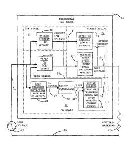
Figure 1 is a diagram of a power supply unit 11 for a thermostat needing low
power. Unit 11 may have a triac or SCR module 12 having an input connected to
a
line voltage 13. Module 12 may have a relay or some triggerable switch. A
MOSFET power steal module 14 may have an input connected to an output of
module
12 via line 21. An output of module 14 may be connected to a load voltage line
15.
A source 10 may provide AC power on line voltage 13 and line 16. Line 16 may
be
connected to one end of an electric baseboard 17. Another end of baseboard 17
may
be connected to line 15.
A bypass circuit 18 may have an input connected to line voltage 13. An
output of circuit 18 may be a circuit low voltage line 21 connected to an
input of
stealing circuit 19. Unit 11 layout may be divided into three areas including
an on
state area 22, an off state area 23, and an always active area 24. Modules 12
may be
in area 22. Circuit 18 may be in area 23, and circuit 19 and 14 may be in area
24. A
component of the triac or SCR module 12 may be a triac. Components of the
MOSFET power steal module 14 may incorporate power steal switching MOSFETs.
A component of bypass circuit 18 may be an RC network. A component of stealing
circuit 19 may be for energy storage.
Figure 2 is a diagram of a power supply unit 31 for a thermostat needing more
power like RF applications. Unit 31 may be similar to unit 11 of Figure 1
except that
the component of circuit 18 may instead be an AC-DC converter and the MOSFET
power steal module is in the area 22.
Figure 3 is a diagram of a power supply unit 41 for a thermostat needing low
power. Unit 41 may be similar to unit 11 of Figure 1 except that unit 41 may
incorporate a zero crossing (ZC) detection module 26 in area 22. An input of
module
26 may be connected to line voltage 13. An output from module 26 may be a ZC
signal on a line 27 to an input of a gate driving circuit 28. Also to an input
of circuit
28 may be the circuit low voltage on line 21. An output from circuit 28 may go
to an
input of module 14 via a line 29. Module 26 may incorporate a half wave ZC
detect
component. Circuit 28 may incorporate a MOSFET gate signal shaping component.
Page 5
CA 02849789 2014-04-17
=
Figure 4 is a diagram of a power supply unit 51 for a thermostat needing high
power for RF applications. Unit 51 may be similar to unit 41 of Figure 3
except that
the component of circuit 18 may instead be an AC-DC converter and the MOSFET
power steal module is in the area 22.
Figure 5 is a diagram of a power supply unit 61 for a thermostat using low
power. Unit 61 may be similar to unit 41 of Figure 3 except that unit 61 does
not
necessarily incorporate the gate driving circuit 28 and may incorporate a
microcontroller 32 and an active trigger module 33 in area 22. ZC signal may
go on
line 27 to an input of microcontroller 32. A drive signal on a line 34 may go
to an
input of active trigger module 33. Stored energy may proceed from an output of
circuit 19 to an input of module 33 via a line 35. A trig signal from an
output of
module 33 may proceed along a line 36 to an input of module 12.
Figure 6 is a diagram of a power supply unit 71 for a thermostat needing high
power. Unit 71 may be similar to unit 61 of Figure 5 except that the component
of
circuit 18 may be an AC-DC converter and the MOSFET power steal module is in
the
area 22. Units 61 and 71 may be expanded to incorporate the gate driving
circuit 28
arrangement of units 41 and 51.
Figure 8 is a diagram of a low power version of a power supply unit 81 having
resemblances to units 11, 31, 41, 51, 61 and 71 of Figures 1-6, respectively.
An RC
network of a bypass circuit 18 may output current along connection 21 to power
stealing switching MOSFETs. Power steal module 14 along connection 52 may
provide stolen energy (Vrect) to energy storage module or stealing circuit 19.
A
connection 53 may provide energy at a level (Vrect) 10 or 15 Vdc to a linear
regulator
and super cap circuit 54, the gate driving circuit of MOSFET signal shaping
circuit
28, a DC-DC negative current source 55 of active trigger module 33, and a
backlight
circuit 56.
Regulator and super cap circuit 54 may provide 3 Vdc power along connection
57 to a processor and other circuits 58. Zero crossing detector 26 having an
input
along connection 66 from bypass circuit 18 and a half wave ZC detect of
detector 26
may provide a zero crossing signal along a connection 27 to a CPU 32. A drive
signal
from CPU 32 along a connection 34 may go to a triac gate triggering signal
circuit 59
of active trigger module 33. The DC-DC negative current source 55 may provide
energy at Vo with a current of a negative 300mA along a connection 61 to the
triac
gate triggering signal circuit 59.
Page 6
CA 02849789 2014-04-17
A zero crossing signal may go on connection 62 from detector 26 to the gate
signal shaping circuit 28. A MOSFET reverse wave protection circuit 63 may
have
an input from line 13 and a protect signal output on connection 64 to circuit
28.
Figure 9 is a diagram of a high power version of a power supply unit 91 which
appears similar to unit 81 of Figure 8. Line power 13 of other units may be
presented
as two lines 1 and 2 at unit 91. Power 71 of line 1 may be provided to power
steal
module 14 and MOSFET reverse wave protection circuit 63. Power 72 of line 2
may
be provided to bypass circuit 18 and half wave ZC detector of circuit 26.
In contrast to unit 81, bypass circuit 18 of unit 91 may have an AC-DC
converter in lieu of an RC network. AC-DC converter may supply energy (Vrect)
on
connection 21 to energy storage module 19. In lieu of linear regulator and
super cap
circuit 54, unit 91 may have a DC-DC converter 67. An output of converter 67
may
be 3 Vdc to processor and circuits 58 and RF RedlinkTM module 68. RF RedlinkTM
module 68 may also be a Wifi module or any other RF protocol. Another
distinction
between units 81 and 91 may be connection 36 being extended as an input to
gate
signal shaping circuit 28.
Figures 10-17 are diagrams for circuitry of various parts of unit 81. Figure
10
is a diagram of power steal switching MOSFETs 14 showing a line 1, which may
be
of power 13 and be designated as line 71. Also, there may be connections 29
and 52,
and ground terminal 75. Figure 11 is a diagram of energy storage module 19 and
linear regulator 54. Also shown are connections 52, 53 and 57, and ground
terminal
75.
Figure 12 is a diagram of a triac circuit 12 and an RC network of bypass
circuit 18 along with line 2, which may be of power 13 and designated as line
72.
Also there may be connections 66 and 36, and ground terminal 75. Figure 13 is
a
diagram of a half wave ZC detect circuit 26 along with connections Vrect 53, a
connection 66, crossing connection 62, CPU ZC connection 27, and ground
terminal
75.
Figure 14 is a diagram of the gate signal shaping circuit 28. Also shown are
connections 53, 62, 64 and 29, and ground terminal 75. Figure 15 is a diagram
of a
MOSFET reverse wave protection circuit 63 showing connection 53, line 71,
connection 64 for the protect signal, and a ground terminal 75.
Figure 16 is a diagram of the DC-DC negative current source 55 having an
output on connection 61, a voltage connection 53 and a ground connection 75.
Figure
Page 7
CA 02849789 2014-04-17
17 is a diagram of triac gate triggering signal circuit 59 showing a
connection 61, a
drive connection 34, a triac gate signal connection 36 and a ground connection
75.
Power supply unit 91 of the high power version may be essentially the same as
power supply unit 81 of the low power version. The following noted Figures may
reveal some differences between the units. Figure 18 is a diagram of a high
power
version of bypass circuit 18 having an AC-DC converter in lieu of an RC
network as
shown in Figure 12. The AC-DC converter may be connected to a crossing signal
on
connection 62, a voltage connection 53, a line 72 connection from an output of
triac
12, an energy output on connection 21 and a ground connection 75. Figure 19 is
a
diagram of a DC-DC converter 67 in lieu of the linear regulator of Figure 11.
Converter 67 may have a connection 53 from the energy storage module 19, an
output
on connection 57 and a ground connection 75.
Figure 20 is a diagram of a half wave ZC detect circuit 26 for the unit 91
high
power version in lieu of circuit 26 of Figure 13. The design of circuit 26 in
Figure 20
may be different from circuit 26 in Figure 13 in that circuit 26 of Figure 20
is
designed to accommodate a line 72 connection. Circuit 26 may have output lines
on
connection 62 and 27. Circuit 26 may have a voltage connection 53 and a ground
connection 75.
Figure 21 is a diagram of gate shaping signal circuit 28 for the unit 91 high
power version in lieu of circuit 28 of Figure 14. The design of circuit 28 in
Figure 21
may be different from circuit 28 in Figure 14 in that circuit 28 of Figure 21
is
designed to accommodate a drive signal on connection 36. Circuit 28 may also
have
input lines on connections 53, 62 and 64. There may also be a gate signal
output on
connection 29. Circuit 28 may have a ground connection 75.
A thermostat power supply may incorporate a first terminal for connection to a
first line of a power source, a triac having a first input connected to the
first terminal,
a bypass circuit having a first input connected to the first terminal, a
stealing circuit
having an input connected to an output of the bypass circuit, a power steal
module
having an input connected to an output of the triac and an output connected to
an
output of the stealing circuit, a second terminal for connection to a load, a
zero
crossing detection module having an input connected to the first terminal, and
a gate
driving circuit having an input connected to an output of the zero crossing
detection
module, and an output connected to a second input of the power steal module.
Page 8
CA 02849789 2014-04-17
The power steal module may be for stealing energy from the first terminal.
The stealing circuit may be for storing stolen energy from the power steal
module.
The power steal module may incorporate one or more MOSFETs that switch on and
off for stealing energy. The gate driving circuit may provide gate signals to
the one or
more MOSFETs for switching the one or more MOSFETs on and off.
The gate driving circuit may shape the gate signals to reduce EMI emissions
from the one or more MOSFETs due to switching the one or more MOSFETs on and
off. The zero crossing detection module may provide a signal to the gate
driving
circuit for determining times that the gate signals are to switch the one or
more
MOSFETs on and off relative to a zero crossing point of a waveform on the
first line
of the power source.
A power unit may incorporate a first terminal for connection to a power
source, a triggerable switch having an input connected to the first terminal,
a bypass
circuit having an input connected to the first terminal, a storage having an
input
connected to an output of the bypass circuit, a power steal module having an
input
connected to an output of the triggerable switch and having an output
connectable to a
second terminal, a second terminal for connection to a load connected to the
power
source, a zero crossing detector having an input connected to the first
terminal, and a
gate driving circuit having an input connected to the zero crossing detector,
and
having an output connected to the power steal module.
The power steal module may incorporate one or more transistors that switch
on and off to let current flow as deemed to the second terminal. The gate
driving
circuit may provide signals to the one or more transistors that switch on and
off
according to the signals which are adjusted in shape to result in the switch
on and off
of current to obtain minimized EMI emissions from switched current. The
minimized
EMI emissions are to comply with applicable government regulations. The one or
more transistors may be MOSFETs.
The power steal module and/or gate driving circuit may further incorporate
MOSFETs as the one or more transistors, one or more current limiting devices
to
control a rate of charge and discharge of one or more gates of the MOSFETs,
and
latching circuitry enabled by a voltage level detector to keep a state of the
MOSFETs
from a previous power steal to a subsequent power steal.
The unit may further incorporate a MOSFET wave protection module having
an input connected to the first terminal and an output connected to an input
of the gate
Page 9
CA 02849789 2014-04-17
signal generator. The gate signal generator may provide the signals to the one
or
more transistors according to timing derived from the zero crossing detector.
A thermostat power system may incorporate a first terminal for connection to
a power supply and load arrangement, a second terminal for connection to the
power
supply and load arrangement, a triggerable switch, having an input, connected
to the
first terminal, a bypass circuit having an input connected to the first
terminal, an
energy storage module having an input connected to an output of the bypass
circuit, a
power steal module having an input connected to an output of the triggerable
switch,
and a driving circuit for a control signal having an output connected to a
second input
of the power steal module. The control signal may minimize EMI emissions from
the
power steal module.
The system may further incorporate a wave zero crossing detector having an
input connected to the first terminal and an output connected to an input of
the driving
circuit.
The control signal from the driving circuit may goes to a gate of one or more
transistors to turn on or off the one or more transistors to steal power. The
turn on or
off of the transistors may cause EMI emissions. The driving circuit adjusts a
shape of
the control signal to turn on or off the transistors in a manner to minimize
EMI
emissions. The one or more transistors may be MOSFETs.
The driving circuit may provide a control signal that is timed according to a
signal from the wave zero crossing detector to turn on or off the transistors
in a
manner to minimize EMI emissions.
The triggerable switch may be selected from a group consisting of a triac, an
SCR and a relay.
The system may further incorporate a reverse wave protection module having
an input connected to the first terminal and an output connected to a second
input of
the driving circuit.
A power supply unit for a heating, ventilation and air conditioning
thermostat,
may incorporate a first terminal for connection to a line of a power source, a
second
terminal for connection to a load, a bypass circuit having an input connected
to the
first terminal, a triac having an input connected to the first terminal, a
stealing circuit
having an input connected to an output of the bypass circuit and having an
output
connected to the second terminal, a power steal module having an input
connected to
Page 10
CA 02849789 2014-04-17
an output of the triac, and a trigger circuit having an output connected to a
second
input of the triac.
The unit may further incorporate a zero crossing detection circuit having an
input connected to the first terminal and an output connected to an input of
the trigger
The unit may further incorporate a zero crossing detection circuit having an
input connected to the first terminal, and an interface circuit having an
input
connected to an output of the zero crossing detection circuit and having an
output
connected to an input of the trigger circuit.
A second output of the stealing circuit may be connected to a second input of
the trigger circuit. An output of the trigger circuit may be connected to a
second input
of the triac. The stealing circuit may incorporate energy storage. Stored
energy may
go from the second output of the stealing circuit to the second input of the
triac.
A zero crossing signal may go from the zero crossing detection circuit to the
The zero crossing detection circuit may incorporate a half wave zero crossing
detector. The trigger circuit may incorporate a DC-DC negative current source
having an input connected to the second output of the stealing circuit, and a
triac gate
The unit may further incorporate a DC-DC converter connected to the second
output of the stealing circuit. The bypass circuit may incorporate an AC-DC
converter.
25 The unit may further incorporate a linear regulator connected to the
second
output of the stealing circuit. The bypass circuit may incorporate an RC
network.
A power system for thermostats, may incorporate a first terminal connected to
a line of a power supply, a bypass circuit having an input connected to the
first
terminal, a triggerable switch having an input connected to the first
terminal, a power
Page 11
CA 02849789 2014-04-17
crossover detector and having an output connected to a second input of the
triggerable
switch.
The trigger circuit may incorporate a processor. The processor may have an
input connected to the output of the zero crossover detector and an output
connected
to the second input of the triggerable switch. The processor may determine a
drive
signal for the triggerable switch from a zero crossing signal of the output of
the zero
crossover detector and from a set of instructions.
Power may be taken from the energy storage module and used to trigger the
triggerable switch near a zero crossing of energy on the line of the power
supply as
effected by the processor and a line pattern according to a working quadrant
of the
triggerable switch.
The system may further incorporate a gate signal shaper having an input
connected to an output of the zero crossover detector and having an output
connected
to the power steal module. The power steal module may incorporate one or more
MOSFETs.
An output of the gate signal shaper may be a gate signal having a shape that
switches the one or more MOSFETs on or off in a manner to minimize EMI
emissions from switching stolen power by the one or more MOSFETs.
The system may further incorporate a MOSFET reverse wave protection
circuit having an input connected to the first terminal and an output
connected to a
second input of the gate signal shaper.
The power steal module may steal power from the first terminal or an output
of the bypass circuit. The power steal module may provide stolen power to the
energy
storage module.
A thermostat power system may incorporate a triggerable switch having an
input connected to a first terminal, a bypass circuit having an input
connected to the
first terminal, an energy storage module having an input connected to an
output of the
bypass circuit and an output connected to a second terminal, a power steal
circuit
having an input connected to an output of the triggerable switch, and an
active trigger
module having an input connected to an output of a wave position detector,
having an
output connected to the triggerable switch, and having an input connected to a
second
output of the energy storage module. The first terminal and second terminal
may be
for connection to an AC power line and load arrangement.
Page 12
CA 02849789 2014-04-17
The power steal circuit may incorporate transistors. A trig signal may be sent
at certain times, according to information at the output of the wave position
detector,
from the output of the active trigger module to a second input of the
triggerable
switch. A signal from the output of the triggerable switch to the input of the
power
steal circuit may turn the transistors on or off. The active trigger module
may take
energy at the second input from the second output of the energy storage to
trigger the
triggerable switch near a zero crossing of the power line when energy directly
from
the power line is insufficient to trigger the triggerable switch.
A power supply unit for a heat, ventilation and air conditioning thermostat,
may incorporate a triac having an input, a gate and an output, a bypass
circuit having
an input connected to the input of the triac, a stealing circuit having an
input
connected to an output of the bypass circuit, and a MOSFET power steal module
having an input connected to the output of the triac. The input of the triac
and an
output of the MOSFET power steal module may be primary terminals for
connection
in a power circuit.
The power circuit may incorporate a power source connected in series with an
electrical load. The electrical load may be an electric heating mechanism.
The stealing circuit may incorporate an energy storage module. The MOSFET
power steal module may steal energy and the energy may go to the energy
storage
module. The energy may be used to trigger the triac at a zero crossing of line
voltage
from the power source.
The unit may further incorporate a gate signal shaper connected to the
MOSFET power steal module. The gate signal shaper may provide a gate signal
that
results in a soft transition of turning on and off of the MOSFETs.
The unit may further incorporate a half wave zero cross detect module
connected to the line voltage, to a gate signal shaper, and to a triac gate
triggering
module.
Power supply electronics for a thermostat, may incorporate a first terminal
for
connection to a first line of a power source, a bypass circuit having an input
connected
to the first terminal, a triac having an input connected to the first
terminal, a second
terminal for connection to a load, a stealing circuit having an input
connected to an
output of the bypass circuit and an output connected to the second terminal,
and a
power steal module having an input connected to the output of the triac and an
output
connected to the second terminal.
Page 13
CA 02849789 2014-04-17
The power steal module may incorporate one or more MOSFETs that are
switched on to steal power. The stealing circuit may incorporate an energy
storage
unit. Stolen power goes to the energy storage unit.
The bypass circuit may incorporate an RC network, or an AC-DC converter.
The electronics may further incorporate a linear regulator and a super
capacitor connected to an output of the energy storage unit.
The electronics may further incorporate a DC-DC converter connected to an
output of the energy storage unit.
If the power steal module incorporates two or more MOSFETs, then a serial
A thermostatic power supply may incorporate a bypass circuit, a first terminal
for connection to a power source, a second terminal for connection to a load,
a bypass
circuit having an input connected to the first terminal, an energy storage
module
having an input connected to the bypass circuit and an output connected to the
second
The supply may further incorporate a DC-DC converter having an input
connected to the output of the energy storage module. The bypass circuit may
The supply may further incorporate a linear regulator having an input
connected to the output of the energy storage module. The bypass circuit may
incorporate an RC network.
The supply may further incorporate a super capacitor connected to the linear
In the present specification, some of the matter may be of a hypothetical or
prophetic nature although stated in another manner or tense.
30 Although the present system and/or approach has been described with
respect
to at least one illustrative example, many variations and modifications will
become
apparent to those skilled in the art upon reading the specification. It is
therefore the
intention that the appended claims be interpreted as broadly as possible in
view of the
related art to include all such variations and modifications.
Page 14