Note: Descriptions are shown in the official language in which they were submitted.
CA 02849807 2014-03-24
WO 2013/155670 PCT/CN2012/074136
1
STANDBY POWER SUPPLY CIRCUIT FOR 2-WIRE BUS INTERCOM SYSTEM AND
APPARATUS THEREOF
FIELD OF THE INVENTION
The invention relates to the intercom system technical field, and more
particularly to a standby power supply circuit for a 2-wire bus intercom
system
and an apparatus thereof.
BACKGROUND OF THE INVENTION
In order to implement a 2-wire video intercom system, the direct current
power, the video carrier signal, the audio signal and the command data signal
have to be transmitted on a common 2-wire bus simultaneously. Therefore, the
power supply circuits of the system power supply and devices thereof have to
comprise an inductance component connected to the common bus in series,
which allows the direct current passing whilst also suppresses the alternating
current signal. However, it is common sense to the skilled person in art that
the
audio signal frequency is low to 300Hz if a coil inductor is used as the
inductance component. In order to achieve the sufficient impedance and power
supply capacity as well, the size of such inductor shall become very large.
Fig.1
illustrates a circuit diagram of a power supply circuit for a 2-wire bus
intercom
system according to the prior art. As shown in Fig.1, an electronic inductance
circuit can be usually used to replace the coil inductor to reduce its size.
In
detail, Figs.2a-2d individually illustrate a circuit diagram of 4 conventional
power
supply circuits for a 2-wire bus intercom system according to the prior art.
However, there is only one system power supply for a 2-wire intercom system in
a building; hence, even for a large 2-wire intercom system with large numbers
of device loads, it only allows a very small number of devices at operating
status whilst the absolute majority of the device loads have to be at standby
status.
As above described, the conventional power supply circuits for a 2-wire
intercom system are consisted of an electronic inductance circuit and a
voltage
CA 02849807 2014-03-24
WO 2013/155670
PCT/CN2012/074136
2
regulator circuit, which offer power to both standby circuits and operation
circuits. While the alternating current impedance of an electronic inductance
circuit is limited, especially a large current power supply with an electronic
inductance circuit for an operation circuit. However, all the device loads of
a
2-wire intercom system are connected to the common bus in series, which
means the alternating current impedance of n device loads is 1/n of one device
load. When the quantity of device loads is large, the alternating current
impedance will become insufficient, the size of 2-wire intercom system will be
limited and the audio quality of such 2-wire intercom system will become much
worse.
Consequently, existing solutions including the prior art mentioned above
can't achieve a higher alternating current impedance at the standby status
when the 2-wire bus intercom system is connected with large amount of device
loads. Due to the above mentioned problems, the present invention is to
propose a standby power supply circuit for a 2-wire bus intercom system and an
apparatus thereof.
SUMMARY OF THE INVENTION
The main object of the present invention is to provide a power supply circuit
with sufficiently large alternating current impedance for 2-wire bus intercom
system even at standby status. Hence, the present invention provides a
standby power supply circuit for a 2-wire bus intercom system and an apparatus
thereof.
According to an aspect of the present invention, it provides a standby
power supply circuit for a 2-wire bus intercom system. The standby power
supply circuit is separated into two power supply modules; in which the first
power supply module is a power supply to standby circuit and the second power
supply module is a power supply to operation circuit; the power supply to
operation circuit is switched off by a constant current switch when the device
load is at the standby status; and the power supply to standby circuit
comprises
a constant current circuit whose alternating current impedance is very large.
CA 02849807 2014-03-24
WO 2013/155670
PCT/CN2012/074136
3
According to another preferred embodiment of the present invention, the
power supply to standby circuit further comprises a constant current circuit
connected between the input terminal and a standby regulator circuit.
According to another preferred embodiment of the present invention, the
constant current circuit further comprises a main constant current circuit and
an
auxiliary constant current circuit, in which the main constant current circuit
is
configured to make the current through the main constant current path stable;
and the auxiliary constant current circuit is configured to offer an enough
bias
current for the main constant current circuit under a rather lower bias
voltage
and maintain an rather larger AC.
According to another preferred embodiment of the present invention, main
constant current circuit further comprises a main constant current path and a
voltage regulator unit, in which the voltage regulator unit is configured to
make
the voltage stable whatever the temperature or current fluctuates and make the
alternating current impedance of the main current path very high.
According to another preferred embodiment of the present invention, main
constant current path is along a first transistor and a first resistor; in
which the
collector of the first transistor is connected to the input terminal and the
emitter
of the first transistor is connected with the first resistor in series.
According to another preferred embodiment of the present invention,
voltage regulator unit further comprises: a diode and a first Zener diode
conversely connected in series, a second resistor and a first capacitor
connected in series; and the diode and the first Zener diode connected with
the
second resistor and the first capacitor in parallel.
According to another preferred embodiment of the present invention, the
standby regulator circuit further comprises a set of resistors consisted of a
third
resistor and a forth resistor connected in series, a second Zener diode and a
second capacitor; and the set of resistors, the second Zener diode and the
second capacitor are connected in parallel and grounded.
According to another preferred embodiment of the present invention, the
voltage regulator unit further comprises a first capacitor and a first Zener
diode
connected in parallel.
According to another preferred embodiment of the present invention, the
standby regulator circuit further comprises a second Zener diode and a second
CA 02849807 2014-03-24
WO 2013/155670
PCT/CN2012/074136
4
capacitor connected in parallel and grounded.
According to another preferred embodiment of the present invention, the
auxiliary constant current circuit comprises a control current path and a
second
control current path, in which the control current path is along a second
transistor and a fifth resistor; the second control current path is along a
third
resistor and a sixth transistor; the fifth resistor is connected to the base
and the
emitter of the third transistor in parallel; and the sixth resistor is
connected to
the collector and the base of the second transistor in parallel.
According to another preferred embodiment of the present invention, the
auxiliary constant current circuit further comprises a third capacitor
connected
to the collector and the emitter of the third transistor in parallel.
According to another preferred embodiment of the present invention, the
standby power supply circuit further comprises a MCU, configured to control
the
constant current switch to be switched on/off.
According to another preferred embodiment of the present invention, the
power supply to operation circuit further comprises an electronic inductance
circuit and a second voltage regulator circuit.
According to another preferred embodiment of the present invention, the
constant current switch is connected between the power supply to standby
circuit and the power supply to operation circuit, configured to switch off by
the
power supply to operation circuit when the device load is at the standby
status.
According to another preferred embodiment of the present invention, the
constant current switch further comprises at least two transistors, three
resistor
and a forth capacitor, in which the seventh resistor is connected to the
emitter
and the base of the forth transistor in parallel; the base of the forth
transistor is
connected to the collector of the fifth transistor; the eighth resistor is
connected
between the emitter of the fifth transistor and the ground; and the forth
capacitor
is connected between the base of the fifth transistor and the ground.
According to another preferred embodiment of the present invention, the
collector of the forth transistor is connected to the electronic inductance
circuit;
and the ninth resistor is connected to the base of the fifth transistor and a
MCU.
According to another preferred embodiment of the present invention, the
electronic inductance circuit comprises: a main circuit path along an inductor
and a source terminal and a drain terminal of a FET between the input terminal
CA 02849807 2014-03-24
WO 2013/155670
PCT/CN2012/074136
and the output terminal of the electronic inductance circuit, in which the
inductor
is connected to the source terminal of the FET; a resistor and a freewheeling
diode individually connected to the inductor in parallel; and a secondary
circuit
path along a capacitor connected with a second resistor in series between the
5 input terminal and the output terminal, which is connected to the main
circuit
path in parallel.
According to another preferred embodiment of the present invention, the
inductor and the FET are connected in series, and the node between the
capacitor and the second resistor is connected with the gate terminal of the
FET.
According to another preferred embodiment of the present invention, the
FET is a P-channel FET, and the drain terminal of the P-channel FET is
connected to the output terminal; and the inductor is connected between the
input terminal and the source terminal of the P-channel FET.
According to another preferred embodiment of the present invention, the
FET is an N-channel FET, and the source terminal of the N-channel FET is
connected to the input terminal; and the inductor is connected between the
source terminal of the N-channel FET and the output terminal.
According to another aspect of the present invention, it provides an
apparatus for a 2-wire bus intercom system. The apparatus comprises any one
of the standby power supply circuits above mentioned.
Embodiments of the present invention provide a standby power supply
circuit for a 2-wire bus intercom system and an apparatus thereof, which
achieves larger alternating current impedance at standby status and high audio
quality for a 2-wire bus intercom system.
BRIEF DESCRIPTION OF THE DRAWINGS
The subject matter of the invention will be explained in more details in the
following description with reference to preferred exemplary embodiments which
are illustrated in the drawings, in which:
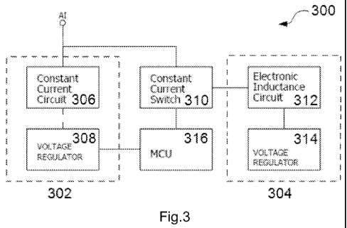
Fig.1 illustrates a circuit diagram of a power supply circuit for a 2-wire bus
intercom system according to the prior art;
CA 02849807 2014-03-24
WO 2013/155670
PCT/CN2012/074136
6
Figs.2a-2d individually illustrate a circuit diagram of 4 conventional power
supply circuits for a 2-wire bus intercom system according to the prior art;
Fig.3 illustrates a circuit diagram of a standby power supply circuit for a
2-wire bus intercom system according to a preferred embodiment of the present
invention;
Fig.4 illustrates a standby power supply circuit for a 2-wire bus intercom
system according to a preferred embodiment of the present invention;
Fig.5 illustrates a standby power supply circuit for a 2-wire bus intercom
system according to another preferred embodiment of the present invention;
Fig.6 illustrates a circuit diagram of a kind of the electronic inductance
circuit with a P-channel FET for the power supply of a 2-wire bus intercom
system according to a preferred embodiment of the present invention; and
Fig.7 illustrates a circuit diagram of a kind of the electronic inductance
circuit with an N-channel FET for the power supply of a 2-wire bus intercom
system according to another embodiment of the present invention.
DETAILED DESCRIPTION OF PREFERRED EMBODIMENTS
Exemplary embodiments of the present invention are described in
conjunction with the accompanying drawings hereinafter. For the sake of
clarity
and conciseness, not all the features of actual implementations are described
in
the specification.
Fig.3 illustrates a circuit diagram of a standby power supply circuit for a
2-wire bus intercom system according to a preferred embodiment of the present
invention.
As shown in Fig.3, the standby power supply circuit 300 for a 2-wire
intercom system of the present invention is separated into two power supply
modules: a power supply to standby circuit 302 and a power supply to operation
circuit 304, the power supply to standby circuit 302 comprises a constant
current circuit 306 connected between the input terminal Al and a standby
regulator circuit 308. The constant current switch 310 is connected between
the
power supply to standby circuit 302 and the power supply to operation circuit
304 and configured to switch off by the power supply to operation circuit 304
CA 02849807 2014-03-24
WO 2013/155670
PCT/CN2012/074136
7
when the device load is at the standby status.
As the operation power supply circuit 304 is switched off when the device
load is at standby status, the number of this circuit 304 connected to the
system
common bus simultaneously is very small. The alternating impedance of the
electronic inductance circuit 310 is not very large, but the alternating
current
impedance affection on this circuit 304 is less.
The power supply to operation circuit 304 comprises an electronic
inductance circuit 312 and a second voltage regulator circuit 314. It's
obvious to
the person skilled in art that electronic inductance circuit 312 and the
second
voltage regulator circuit 314 can be any available electronic inductance
circuits
and voltage regulator circuits according to the prior art.
According to a preferred embodiment of the present invention, the standby
power supply circuit 300 further comprises a MCU 316 which is configured to
instruct and control the constant current switch 310 to be switched on/off.
Fig.4 illustrates a standby power supply circuit for a 2-wire bus intercom
system according to a preferred embodiment of the present invention.
As shown in Fig.4, the standby power supply circuit 400 comprises a main
constant current circuit 402, an auxiliary constant current circuit 404, a
constant
current switch 406, a standby regulator circuit 408 and a power supply to
operation circuit 410. Especially the constant current circuit 306 in Fig.3
further
comprises a main constant current circuit 402 and an auxiliary constant
current
circuit 404, in which the main constant current circuit is 402 configured to
make
the main constant current 11 through said main constant current path stable;
and the auxiliary constant current circuit 404 is configured to offer an
enough
bias current for the main constant current circuit under a rather lower bias
voltage (e.g. 5-10V), furthermore, to maintain an rather larger AC impedance
(e.g. about 100kO). In an actual embodiment, the desired AC impedance of the
whole constant current circuit is about 80k0, if the auxiliary constant
current
circuit is directly replaced by a 80kO resistor, a bias voltage more than 100V
shall be utilized to offer a lmA current for constant bias circuit.
In detail, the main constant current circuit 402 further comprises a main
constant current path and a voltage regulator unit configured to make the
voltage stable whatever the temperature or current fluctuates and make the
alternating current impedance of said main current path very high; in which
the
CA 02849807 2014-03-24
WO 2013/155670
PCT/CN2012/074136
8
main constant current path is along a transistor Q3 and a resistor R3,
moreover
the collector of the transistor Q3 is connected to the input terminal Al and
the
emitter of the transistor Q3 is connected with the resistor R3 in series.
As to voltage regulator unit, it further comprises a diode D1 and a Zener
diode U1 or a similar device (e.g. a TL431) conversely connected in series, a
resistor R4 and a capacitor 02 connected in series; and the diode D1 and the
Zener diode U1 connected with the resistor R4 and the capacitor 02 in parallel
between the auxiliary constant current circuit 404 and the standby regulator
circuit 408.
The auxiliary constant current circuit 404 comprises a control current path
and a second control current path, in which the control current path is along
a
the NPN transistor Q1 and a resistor R2, the second control current path is
along a resistor R1 and a NPN transistor Q2, the resistor R2 is connected to
the
base and the emitter of the transistor Q2 in parallel, the resistor R1 is
connected
to the collector and the base of the transistor Q1 in parallel and the base of
the
transistor Q1 is connected to the collector of the transistor Q2 whilst the
base of
the transistor Q2 is connected to the emitter of the transistor Ql.
Furthermore, a
capacitor 01 is connected to the collector and the emitter of the transistor
Q2 in
parallel.
The constant current switch 406 is connected between the auxiliary
constant current circuit 404 and the power supply to operation circuit 410,
and
configured to switch off by said power supply to operation circuit when the
device load is at the standby status. In detail, the constant current switch
406
further comprises at least two transistors, three resistor and a forth
capacitor, in
which the resistor R9 is connected to the emitter and the base of the PNP
transistor Q5 in parallel; the base of the transistor Q5 is connected to the
collector of the NPN transistor Q4; the resistor R8 is connected between the
emitter of the transistor Q4 and the ground; and the capacitor 04 is connected
between the base of the transistor Q4 and the ground.
It's optimal that the constant current switch 406 is connected to MCU 412
via a resistor R7.
The standby regulator circuit 408 further comprises a set of resistors
consisted of a resistor R5 and another resistor R6 connected in series, a
Zener
diode U2 (e.g. a TL431) and a capacitor 03; and the set of resistors R5 and
R6,
CA 02849807 2014-03-24
WO 2013/155670
PCT/CN2012/074136
9
the Zener diode U2 and the capacitor 03 are connected to the main constant
current circuit 402 in parallel and grounded.
Taking the embodiment shown in Fig.3 as an example, the standby power
supply circuit of the present invention is structured by a main constant
current
circuit and an auxiliary constant current circuit; wherein the main constant
current circuit has a voltage regulator unit ZDI, whose voltage is stable even
as
the temperature or current fluctuates. Hence, the current 11 via the main
constant current path will be stable and the alternating current impedance of
main current path is very high. Because the main constant current 11 is not
very
small and the voltage regulator unit ZDI also needs a sufficient current to
ensure the voltage stability, so the control current 12 has to be sufficiently
large.
If the control current 12 is supplied by a resistor from the input terminal
Al, the
resistance of such resistor will be not very large; so the alternating current
impedance of the whole constant current will be not very large. For the
constant
current circuit of the present invention, the control current of the main
constant
current is supplied by an auxiliary constant current circuit 12. As the
current 12 is
far smaller than 11, and the auxiliary constant current circuit is structured
by two
transistors back to back, so the control current 13 can be very small and the
resistance of RI can be very large, therefore the alternating current
impedance
of the whole constant current can be kept very large.
Fig.5 illustrates a standby power supply circuit for a 2-wire bus intercom
system according to another preferred embodiment of the present invention.
As shown in Fig.5, the standby power supply circuit 500 also comprises a
main constant current circuit 502, an auxiliary constant current circuit 504,
a
constant current switch 506, a standby regulator circuit 508, a power supply
to
operation circuit 510 and a MCU 512; in which the auxiliary constant current
circuit 504, the constant current switch 506, the standby regulator circuit
508,
the power supply to operation circuit 510 and the MCU 512 can be same or
similar to the auxiliary constant current circuit 404, the constant current
switch
406, the standby regulator circuit 408, the power supply to operation circuit
410
and the MCU 412 of Fig.4. In order to keep the description brief, the same or
similar circuits or components will not be described any more.
The main constant current circuit 502 comprises a main constant current
path and a voltage regulator unit, in which the main constant current path is
CA 02849807 2014-03-24
WO 2013/155670
PCT/CN2012/074136
same or similar to the one in Fig.4, the voltage regulator unit ZD2 is
configured
to make the voltage stable whatever the temperature or current fluctuates and
make the alternating current impedance of the main current path very high.
The voltage regulator unit ZD2 further comprises a capacitor 02 and a
5 Zener diode D1 connected in parallel between the auxiliary constant
current
circuit 504 and the standby regulator circuit 508.
The standby regulator circuit 508 further comprises a Zener diode D2 and a
capacitor 03 connected to the main constant current circuit 502 in parallel
and
grounded.
10 It's obvious to the person skilled in art that, the electronic
inductance circuit
can be a general one or the specific one described as following.
Fig.6 illustrates a circuit diagram of a kind of the electronic inductance
circuit with a P-channel FET for the power supply of a 2-wire bus intercom
system according to a preferred embodiment of the present invention.
As shown in Fig.6, the electronic inductance circuit EL2 comprises a
capacitor 01, a resistor R1, a coil inductor L1, a freewheeling diode D1, a
second resistor R2, a P-channel FET Q1 and a second diode. In detail, a main
circuit path between the input terminal Al and the output terminal AO of the
electronic inductance circuit is along the inductor L1 and the source terminal
as
well as the drain terminal of the P-channel FET Q1, and the inductor L1 and
the
FET Q1 are connected in series. Furthermore, the inductor L1 is connected
between Al terminal and the source terminal of the FET Ql, both the resistor
R1
and the freewheeling diode D1 are individually connected to the inductor L1 in
parallel, the drain terminal of said P-channel FET Q1 is connected to the
output
terminal, and the connection node B1 between the capacitor 01 and the second
resistor R2 is connected to the Gate terminal of the P-channel FET Q1. The
electronic inductance circuit further comprises a second diode connected to
said source terminal and said drain terminal of said FET in parallel. Such
second diode is a general diode embedded in the MOSFET, configured to
prevent the VDS from over-voltage.
Taking the embodiment of Fig.6 as an example, R1 is a key factor of the
AC impedance of the circuit and can be set as about 4.70. In an actual
embodiment, the AC impedance of the circuit is up to about 2k0. As to the
capacitor L1, it shall be chosen to make the AC impedance ZL=2* TE *f*L far
CA 02849807 2014-03-24
WO 2013/155670
PCT/CN2012/074136
11
larger than 4.70 under the 300-3400Hz frequency. For the inductor 01, the
value shall be able to ensure about 300Hz of the filter cutoff frequency. When
connecting Al to a regulated DC power supply and AO to a device load (i.e. a
current load), the voltage across the capacitor 01 can't be changed
transiently.
I.e., Uci = 0, UGS = 0, and Q1 is still turned off. The voltage of AO will be
dropped to the reference GND by device load that IJAI - IJAD = IJAI = UR2, so
the
capacitor 01 will be charged by the resistor R2. When the voltage across 01 is
larger than the gate threshold voltage of the FET Q1, the Q1 starts to be
turned
on. When the current 11 reaches the required current value of the device load,
the charging of the capacitor 01 will be stopped and UGD = 0, therefore, the
voltage drop of electronic inductance EL2 is UEL2 = UAI-UAO = UZ1 +USG.
As the DC resistance value of the coil inductor L1 is far less than the
auxiliary resistor R1, so the AC impedance of Z1 is mainly determined by the
coil inductor L1 that Z1 = Ru//R1 -,--, RLi; therefore, the voltage drop of
the
electronic inductance EL2 is represented by equation (1) as below:
UEL2 = UAI-UAO = 11*RL1+USG (1)
Wherein the DC resistance value of the coil inductor is sufficiently small in
comparison to the resistance value of the resistor R1 that Z1 = RLi//R1 -,--:
RLi.
Next, as to the alternating current impedance of the electronic inductance
EL2, if a fluctuation voltage AU occurs at the terminal of AO, then the
fluctuation
voltage across 01 is AUci = AU*Zci/(R2+Zci). Meanwhile AUci = AUsG-FAURi
= A11/gm+A11*Z1, so AU*Zci/(R2+Zci) =A11/gm+AI1*Z1; therefore R1+41 =
AU/A11 = (1+Z1*gm)*(R2+Zci )/(Zci*gm)={(1+Zl*gm)/gm}*{(R2+Zci )/Zci}
As the alternating current impedance value of coil inductor L1 is much
large than auxiliary resistor, so the alternating current impedance of Z1 is
determined by the auxiliary resistor R1 that Z1 = RLi//R1 P---: R1, so R1+41 =
AU/A11 = (1+Z1*gm)*(R2+Zci )/(Zci *gm) P---: {(1+R1*gm)/gm}*{(R2+Zci )/Zci }
Therefore, the alternating current impedance ZEL2 between the terminals Al
and AO is represented by equation (2) as below:
ZEL2 = (R1+41)//(R2+Zci)
= {(1+Zl*gm)/gm}*{(R2+Zci )/Zci}//(R2+Zci )
-,--: {(1+R1*gm)/gm}*{(R2+Zci )/Zci}//(R2+Zci ) (2)
Wherein, Zci = 1/(j*w*C1) = 1/(j*2*-ef) and "gm" represents the
trans-conductance of the FET.
CA 02849807 2014-03-24
WO 2013/155670
PCT/CN2012/074136
12
When the electronic inductance circuit EL2 allows DC passing, it is
preferable to make the voltage drop UEL2 represented by the equation (1) small
and DC respond quickly. On the other hand, the alternating current impedance
ZEL2 represented by equation (2) shall be sufficiently larger than the cable
loop
resistance of intercom system, what's more it does not change depending on
the change of DC.
It's obvious to the skilled person in art that the electronic inductance
circuit
EL2 can use an N-channel FET to construct the similar circuit as the power
supply of a 2-wire bus intercom system instead of the P-channel FET.
Fig.7 illustrates a circuit diagram of a kind of the electronic inductance
circuit with an N-channel FET for the power supply of a 2-wire bus intercom
system according to another embodiment of the present invention.
As shown in Fig.7, the components of the electronic inductance circuit is
similar to the ones in Fig.6 except for an N-channel FET Ql; therefore, a main
circuit path between the input terminal Al and the output terminal AO of the
electronic inductance circuit is along the drain terminal and the source
terminal
of the N-channel FET Q1 as well as the inductor L1, and the FET Q1 and the
inductor L1 are connected in series. Furthermore, the inductor L1 is connected
between the source terminal of the FET Q1 and AO terminal, both the resistor
R1 and the freewheeling diode D1 are individually connected to the inductor L1
in parallel, the drain terminal of said N-channel FET Q1 is connected to the
input terminal Al, and the connection node B1 between the capacitor C1 and
the second resistor R2 is connected to the Gate terminal of the N-channel FET
Q1. The electronic inductance circuit further comprises a second diode
connected to said source terminal and said drain terminal of said FET in
parallel.
In summary, the circuit shown in Fig.7 is symmetrical to the circuit in Fig.6.
With the circuit shown in Fig.7, the voltage drop and alternating current
impedance between the terminals Al and AO are also applicable to be
represented by the equations (1) and (2) respectively.
According to another aspect of the present invention, it provides an
apparatus which comprises the standby power supply circuit for a 2-wire bus
intercom system mentioned above. Furthermore, it also provides an intercom
system which comprises an apparatus mentioned above.
CA 02849807 2015-11-12
13
Compared with the existing prior arts, the proposed solutions of the present
invention comprise a main constant current circuit and an auxiliary constant
current circuit, which can achieve larger alternating current impedance for
the
2-wire intercom system and offer sufficient power for many device loads both
in
the conditions of operation and standby statuses.
The scope of the claims should not be limited by the preferred embodiments set
forth in the examples, but should be given the broadest interpretation
consistent
with the description as a whole.