Note: Descriptions are shown in the official language in which they were submitted.
CA 02850251 2014-03-27
WO 2013/045424 PCT/EP2012/068835
Aqueous ink formulation containing metal-based nanoparticles for usage in
micro contact printing
The present invention relates to an aqueous formulation containing metal-based
nanoparticles, in
particular silver, especially for generating electrically conductive and/or
optically reflective
structures particularly by microcontact printing, in particular on flexible
and/or transparent
substrates using a stamp made of poly-(dimethylsiloxane). The present
invention further relates to a
method of generating structures, particularly being electrically conductive
and/or optically reflective,
on a substrate by microcontact printing using the above defmed formulation.
The present invention
further relates to a substrate comprising such a structure.
Microcontact Printing ( CP) is touted to be a simple and a versatile printing
process, that employs
micro-patterned stamps, for example made of poly-(dimethylsiloxane) (PDMS) in
order to print
micro scale features onto various substrates. The substrates may include those
being curved and
having a large area. Microcontact printing can be used to print, inter alia,
self assembled monolayers
(SAM's), polymers, dendrimers, catalysts or biomolecules such as proteins,
liposomes, etc. on
substrates of choice. However, there are very few reports on printing
nanoparticles using
microcontact printing. For instance, printing of titanium dioxide (Ti02)
nanoparticles or quantum
dots using microcontact printing have been reported.
By using stamps made of poly-(dimethylsiloxane), furthermore, this material
being a non-polar
elastomer with a hydrophobic surface presents some challenges due to its low
surface energy, thus
resulting in poor wetting of polar ink systems, such as aqueous based ink
systems. Therefore,
methods are known to modify the surface of the poly-(dimethylsiloxane) stamps
in order to increase
the surface energy and furthermore to improve the wetting behavior of polar
ink systems. These
modifying procedures are typically multistep processes involving plasma
treatment and surface
grafting of polar moieties on the poly-(dimethylsiloxane) surface. However,
the surface after the
modification route often presents limited success as the wettability appears
to be getting poor with
repeated usage and/or storage.
An alternative would be to microcontact print metallic colloids directly onto
substrates of choice.
However, there appears to be not much information on printing metallic
nanoparticles using
microcontact printing. For instance, microcontact printing of Pd/Sn or Pd
nanoparticles on poly-
(dimethylsiloxane) stamps was reported as seeds for a further electroless
deposition of NiB or
copper. It has to be noted that the Pd/Sn nanoparticles are only used as seeds
layers and this could as
well be a random deposition of nanoparticles and not really dense structures.
It must also be
highlighted that these seed nanoparticles are often dispersed in organic
solvents like toluene or
hexane.
CA 02850251 2014-03-27
WO 2013/045424 PCT/EP2012/068835
- 2 -
Most of the known printing of metallic conducting pattern was performed by
passivating gold
surfaces by a self assembled monolayer of a suitable thiol followed by
electrodeposition / electroless
deposition of a metallic species on the unpassivated sections of the
substrates and finally a wet
etching to remove the uncoated areas of the gold surface. It is obvious that
this type of patterning is
process intensive and cumbersome.
Known from US 2009/0191355 Al is a method of forming a layer of particulate on
a substrate, and
in particular, a method of forming a thin layer of nanometer sized particulate
on a substrate for use
in microfabrication of components and devices. The method according to this
document generally
comprises the steps of providing an elastomeric stamp having a relief
structure; applying a
composition comprising particulate and a dispersing agent to the relief
structure; selectively
transferring the composition from the relief structure to the substrate to
form the pattern; treating the
composition with charged gas to remove the dispersing agent; and induction
heating to form
functional connection of the particulate. The ink used for performing this
method may contain
conductive materials such as silver and in particular silver nanoparticles, a
binder, and methanol as
solvent.
Document WO 2009/052120 Al describes a method of microfabrication and
nanofabrication of
electrical and mechanical structures at the micron and submicron scale, for
example by microcontact
printing. This method uses a formulation comprising a plurality of metallic
nanoparticles, such as
silver nanoparticles, suspended in a carrier, wherein the carrier comprises
water and at least one
organic solvent miscible with water. The organic solvent being miscible with
water may be an
alcohol, such as terpene alcohol or a polyol, such as glycol or glycerol, or a
long chain alcohol, such
as octanol or decanol. Furthermore, the formulation known from this document
may comprise
additives such as surfactants or dispersants.
However, with respect to the above defmed prior art, the swelling and wetting
behavior has further
potential to be improved especially in absence of surface modification of the
poly-(dimethylsiloxane)
stamp. In detail, a plasma or UV/ozone surface treatment for wetting of the
stamp such as the stamp
made of poly-(dimethylsiloxane) should be avoided.
Consequently, there is the need for further ink formulations improving the
printability and
particularly the wetting behavior especially of a hydrophobic material such as
a poly-
(dimethylsiloxane) stamp without pretreating the stamp. It is thus the object
of the present invention
to provide an aqueous formulation being usable as ink for microcontact
printing which has an
improved wetting behavior of a hydrophobic material such as of a stamp made of
poly-
(dimethylsiloxane).
CA 02850251 2014-03-27
WO 2013/045424 PCT/EP2012/068835
- 3 -
The present invention relates to an aqueous formulation particularly for
generating electrically
conductive and/or reflective structures by microcontact printing,
characterized in that the
formulation contains at least
a) > 15 to < 55 parts by weight water,
b) > 10 to < 50 parts by weight alcohol,
c) > 15 to < 45 parts by weight metal-based nanoparticles,
d) > 0,5 to < 10 parts by weight non-fluorinated surfactant, and
e) > 0,5 to < 10 parts by weight fluorinated surfactant,
wherein the above defmed constituents a) to e) summarize to a concentration of
< 100 parts by
weight in the formulation.
The term "metal-based" nanoparticles in the sense of the present invention
shall particularly mean
any nanoparticles which comprise a metal as such or a compound being at least
partly formed from a
metal compound, such as an alloy, metal oxides or the like. As an example for
metal oxides, titanium
oxide (Ti02) or indium tin oxide (ITO) may be referred to in an exemplary
manner only.
Consequently, at any passage metal-based nanoparticles are cited, these
particles may be metals,
alloys, or metal compounds such as metal oxides. Apart from that, the term
"nanoparticles" in the
sense of the present invention may exemplarily mean particles having a maximum
diameter in a
range of < 250 nm, for example lying in the range of? 1 nm to < 250 nm.
The term "structure" in the sense of the present invention shall particularly
mean any kind of
material being applied to the surface of a substrate. In detail, the term
structure comprises a layer
being applied to a whole or an expanded region of a surface area, such as a
large region coating, or a
defmed pattern being applied just to defmed regions onto the surface of the
substrate.
The term "microcontact printing" according to the present invention shall
particularly mean a
process being generally known in the art. This process comprises the steps of
applying a
formulation, or an ink, respectively, onto a surface or at least onto a part
of the latter of a stamp,
which may be structured or not. The ink being applied to the stamp is in turn
transferred to a suited
substrate in order to apply a structure onto the latter.
CA 02850251 2014-03-27
WO 2013/045424 PCT/EP2012/068835
- 4 -
A formulation according to the present invention overcomes the problems of
wetting without having
to subject a hydrophobic surface, such as a poly-(dimethylsiloxane) surface,
to a lengthy and
cumbersome surface modification procedure. Apart from that, the formulation
according to the
invention does not swell stamps made of a hydrophobic material, such as poly-
(dimethylsiloxane).
Without being bound to the theory it is believed that the positive effects and
advantages being
provided by an aqueous formulation particularly for generating electrically
conductive and/or
reflective coatings according to the invention are obtained by synergistic
effects of the respective
components. Particularly, it is believed that the advantages are obtained by
the components being
present in the formulation according to the invention in a respective
concentration range.
Next to the components defmed above, the ink formulation according to the
invention may comprise
further constituents without leaving the scope of the invention as such. For
example, the formulation
may comprise at least one additive in order to improve one or more of the
properties of the
formulation or to adapt them to the special use. The further one or more
additives being potentially
part of the ink formulation according to the invention may be selected from
the group comprising or
consisting of surfactants, pigments, defoamers, light protecting agents,
lighteners, wighteners,
corrosion inhibitors, antioxidants, algicides, plasticizers, softeners, and/or
thickeners, the list not
being strictly fmal.
The components being present in the ink formulation according to the present
invention are
particularly chosen in view of the wetting behavior on a stamp with regard to
microcontact printing
in a method of generating electrically conductive and/or reflective
structures. Consequently, the
constituents being present in the ink formulation according to the present
invention are particularly
chosen in view of the wetting behavior on hydrophobic materials, such as poly-
(dimethylsiloxane).
Within the in formulation according to the invention, the metal-based
nanoparticles essentially serve
as main ingredient of the particularly electrically conductive and/or
reflective structure to be
generated on the substrate of choice. They may be present in the formulation
according to the
invention in a concentration in the range of? 15 to < 45 parts by weight. It
is clear for one skilled in
the art that either the same kind of nanoparticles may be present in the
formulation according to the
invention, or different kinds of nanoparticles may be present in the
formulation according to the
invention without leaving the invention as such.
The water being present may serve as solvent for dispersing the metal-based
nanoparticles. It may be
present in a concentration in the range of? 15 to < 55 parts by weight.
CA 02850251 2014-03-27
WO 2013/045424 PCT/EP2012/068835
- 5 -
Within the ink formulation according to the present invention, the alcohol may
be present in a
concentration in the range of? 10 to < 50 parts by weight and may serve as co-
solvent. Additionally,
it may take the role as wetting agent.
With respect to the non-fluorinated surfactant, the latter may especially
serve as agent for reducing
the surface tension of the ink, so that the wetting behavior of the stamp may
be further improved. It
may be present in a concentration in the range of? 0,5 to < 10 parts by
weight.
With respect to the fluorinated surfactant, the latter may especially serve as
leveling agent and/or
agent for reducing the surface tension of the ink, providing positive aspects
with respect to the
wetting behavior. It may be present in a concentration in the range of? 0,5 to
< 10 parts by weight
in the formulation.
The ink formulation according to the invention may provide superb wetting
behavior, which is
especially advantageous with respect to microcontact printing. In detail, by
having a good wetting
behavior, the stamp, especially being formed of a hydrophobic material, such
as poly-
(dimethylsiloxane), may be wettened and thus provided with the ink formulation
in a defmed manner.
Consequently, especially in case the stamp is structured in order to generate
a defined structure on a
substrate, a good wetting behavior is advantageous in order to generate the
desired structure by
transferring the ink to the substrate. A structured stamp may thereby
particularly mean a stamp
having at least one surface being provided with a structure. The structure, in
order to be suitable for
microcontact printing, may particularly have protruding and recessed portions
forming the required
structure. The structure as such may be adjusted to the desired application.
It may thus comprise
defmed areas, lines or spots, for example. By addressing the problems known in
the art with respect
to wetting, it may be assured that the desired geometry and form of the
structure to be applied, as
defmed by the stamp or the stamp structure, may accurately be transferred to a
substrate of choice.
It is thereby not necessary to modify the surface of the stamp by chemically
or physically processing
the latter. The wettability may instead be improved by the ink formulation as
such. Consequently, a
printing process may be performed without a further step resulting in a highly
efficient and cost
saving process.
The dimensions and/or structures are furthermore just dependent from the
stamp, or its structure,
respectively, being used and the pressure applied to the latter. Consequently,
by using an ink
formulation according to the present invention, it is possible to print
conducting and/or reflecting
metal structures, for example, in various dimensions.
CA 02850251 2014-03-27
WO 2013/045424 PCT/EP2012/068835
- 6 -
It is also possible to print semi-transparent grid structures, for example
with sheet resistances less
than 5 n/sq., especially if appropriate sintering conditions are chosen after
transferring the
formulation to the substrate. With respect to the electrically conductive
structures being formed on
the substrate of choice, such as conducting paths, or large area coatings,
they may preferably be
temperature resistant, for example at least for a short period of time up to
4000 C, as well as
mechanically flexible. The ink formulation according to the invention may
furthermore be suitable
for generating structures, or lines, respectively, having a width of 100 gm or
less (up to 20 gm or
even lower). This may especially be advantageous with respect to small
dimensioned substrates.
Apart from that, the applicability of the ink formulation according to the
present invention is
especially broad.
Furthermore, the ink formulation according to the present invention is
especially cost-saving to
prepare and to use and, additionally, may provide a superb shelf life.
Furthermore, due to the fact
that the desired structures may appropriately be generated, the degree of
substrate being falsely
coated and thus not being usable for the desired application may be reduced up
to a minimum.
Consequently, the ink formulation according to the present invention may
provide a high efficiency
at its use.
Besides, the ink formulation according to the present invention prevents the
stamp used for printing
from swelling and/or shrinking. In detail, shrinking is a process due to which
the stamp changes its
dimensions leading to the dimensions of the structure being present on the
printing surface of the
stamp as well being changed. Consequently, the printed structure will not have
the dimensions
desired in case the stamp shrinks. Additionally, most organic solvents lead to
a swelling process of a
stamp particularly formed from poly-(dimethylsiloxane), as well having
negative effects to the stamp
and thus to the printing results. These above named disadvantaged may be
prevented by using an
aqueous based formulation according to the present invention.
Even if the ink formulation according to the present invention is particularly
suitable for
microcontact printing and in more detail for microcontact printing using a
hydrophobic stamp, it is
especially suitable for any kind of printing technology employing a
hydrophobic material to transfer
a structure, or a pattern, respectively, to a substrate of choice.
It is the benefit of the present inventors to have found out that the object
of the present invention is
surprisingly solved by a suitable choice of an ink formulation having defmed
constituents
particularly in defmed concentration ranges. The effect according to the
invention is provided,
without being bound to a specific theory, particularly by synergistic effects
of solvents, co-solvents
and surfactants and potentially further additives especially in defmed
concentration ratios.
CA 02850251 2014-03-27
WO 2013/045424 PCT/EP2012/068835
- 7 -
According to an embodiment, the metal-based nanoparticles comprise silver
nanoparticles.
Preferably, all metal nanoparticles are silver nanoparticles. The silver
nanoparticles may preferably
be used, or introduced into the formulation, respectively, in the form of a
silver nanoparticle sol (Ag
sol). The silver nanoparticle sol may be treated and thus particularly
purified and concentrated by
using membrane filtration comprising a filter element with a level of
filtering of 100,00 dalton at
most, for example. The silver nanoparticle sol preferably comprises a
dispersing agent, which may
be formed from a block-copolyether comprising styrene blocks, with 62 parts by
weight C2-
polyether, 23 parts by weight C3-polyether, and 15 parts by weight
polystyrene, with respect to the
dried dispersing agent, with a relation of the length of the blocks C2
polyether to C3 polyether of 7:2
units (for example Disperbyk 190, purchasable by BYK-Chemie, Wesel). By way of
the dispersing
agent, which may serve as capping agent, the silver nanoparticles are
stabilized appropriately.
Consequently, agglomeration of the silver nanoparticles may be prevented.
According to a further embodiment the alcohol may be ethanol, isopropanol,
methanol or a mixture
comprising at least one of the afore-mentioned compounds. Particularly by
using methanol, the
wettability properties of the ink according to the invention were found to be
especially improved.
Furthermore, methanol has a preferred evaporation rate providing a very short
drying time of the
silicone stamp provided with the ink formulation, or the substrate provided
with the structure. Apart
from that, methanol is cost-saving to use and is furthermore non problematic
with respect to its
handling conditions.
According to a further embodiment the metal-based nanoparticles comprise an
average effective
diameter of < 150 nm, particularly of < 100 nm, for example of > 40 nm to < 80
nm, and/or a
bimodal size distribution. The determination of the size, and the size
distribution, respectively, via
laser correlation spectroscopy is known in the art and described, for example,
in T. Allen, Particle
Size Measurements, Bd. L, Kliiver Academic Publishers, 1999. In case silver
nanoparticles are used,
they may preferably be used, or introduced into the formulation, respectively,
in the form of a silver
nanoparticle sol (Ag sol).
The bimodal size distribution may especially be preferred with respect to
electrically conductive
structures such as patterns or coatings, having a low content of metal-based
nanoparticles such as
metal nanoparticles. It is believed that this effect is due to a filling of
the occurring gusset volumes
between larger particles by smaller particles. This results in large and
continuous contact areas to be
formed especially during thermal treatment of the ink formulation applied to
the substrate.
Consequently, the ink formulation according to the invention reaches, with low
content of metal-
based particles, the same electrical conductivity compared to formulations
having a higher content of
CA 02850251 2014-03-27
WO 2013/045424 PCT/EP2012/068835
- 8 -
nanoparticles with monodispers size distributions of the nanoparticles and a
comparable effective
diameter, or even higher electrical conductivities compared to monodispers
size distributions
comprising a comparable amount of metal-based nanoparticles having the same
effective diameter.
Due to the small effective diameter of the metal-based nanoparticles,
structures having a very small
width may additionally be achieved, which is especially preferred for defined
patterns and/or for
compact substrates. Apart from that, a structure may be achieved with a high
contrast.
According to a further embodiment the fluorinated surfactant comprises poly-
(oxetane) polymers
comprising (-C2F5)-groups. These kinds of surfactants provide a plurality of
advantageous
properties. In detail, these surfactants have been found not to bioaccumulate.
There is thus very low
environmental impact because of which these surfactants are environmentally
preferred even if being
fluorosurfactants. Apart from that, the foam being generated may be reduced
due to a reduced air
entrapment because of which these surfactants lead to an improved wetting
behavior and thus
printing result. Furthermore, these surfactants are clear and uniform because
of which they do not
deteriorate the desired appearance of the ink formulation. Generally, flow,
leveling, and surface
appearance may be improved by using the surfactants like described above. The
surfactants used
according to this embodiment are purchasable under the names PolyFox PF-136A,
PF-156A, and
PF-151N from the company Omnova, for example.
According to a still further embodiment the non-fluorinated surfactant
comprises a siloxane, in
particular a polyalkyleneoxide modified heptamethyltrisiloxane. These kinds of
surfactants are
especially preferred wetting agents reducing the surface tension of the ink
formulation according to
this embodiment in an especially preferred manner. Particularly by using these
kinds of non ionic
surfactants, the wetting behavior and thus the distribution of the ink
formulation, for example on a
stamp and essentially independent from the stamp material, may be improved.
For example,
according to this embodiment, the non-fluorinated surfactant may be the one
being purchasable
under its name Silwet L77 from the company GE Silicones.
According to a still further embodiment the formulation contains at least
a) > 31 to < 42, in particular? 36 to < 37 parts by weight water,
b) > 25 to < 35, in particular? 29 to < 31 parts by weight alcohol,
c) > 23,5 to < 33,5, in particular? 28 to < 29 parts by weight metal-based
nanoparticles,
d) > 1 to < 5 in particular? 2,5 to < 3,5 parts by weight non-fluorinated
surfactant, and
e) > 0,5 to < 4,5, in particular? 1,5 to < 3 parts by weight
fluorinated surfactant,
CA 02850251 2014-03-27
WO 2013/045424 PCT/EP2012/068835
- 9 -
wherein the above defmed constituents a) to e) summarize to a concentration of
< 100 parts by
weight in the formulation.
According to this embodiment, especially good results particularly with
respect to microcontact
printing may be achieved. In detail, the wetting behavior of hydrophobic
substrates, such as poly-
(dimethylsiloxane) is especially improved leading to exact and defmed
structures to be formed even
in case the structures have very small dimensions.
It may be seen that the content of solvent and co solvent may be comparable.
For example, the
relation between water and alcohol may be 1/1.
Additionally, the amount of surfactants may be realized to a minor amount so
that the composition
essentially comprises metal-based nanoparticles, such as silver nanoparticles,
water, and alcohol,
such as methanol.
The present invention further relates to a method of generating structures,
particularly being
electrically conductive and/or reflective, on a substrate by microcontact
printing, characterized by
the steps of
A) Providing a stamp;
B) Applying a formulation according to the invention to at least a part of the
surface of the
stamp;
C) Transferring the formulation from the stamp to the substrate; and
D) Optionally treating the formulation transferred to the substrate with heat.
The method according to the invention thus defines a micro printing process
using the ink
formulation according to the invention.
According to step A), a stamp is provided. The stamp may be formed from a
suitable material, such
as a hydrophobic material. However, the advantages such as the wetting
behavior being obtained by
using the formulation according to the invention may generally as well be
achieved by using
substrate. Furthermore, the stamp may comprise a defined pattern in case such
a pattern is to be
applied to the surface of the substrate. For example, the pattern may
correspond to a pattern of
CA 02850251 2014-03-27
WO 2013/045424 PCT/EP2012/068835
- 10 -
conducting lines being required for electrical compounds, and may thus
comprise relief patterns.
This may be realized, for example, by respective protruding and recessed
portions on the surface of
the stamp, like it is known from microcontact printing as such.
According to step B), a formulation according to the invention is applied onto
at least a part of the
surface of the stamp. In detail, the ink formulation is applied to the
printing surface of the stamp and
thus to that surface being used for printing purposes. Consequently, the
formulation is applied to the
surface comprising the desired structure or pattern, respectively by any known
and appropriate
technique thereby wetting the latter. For example, the ink formulation may be
applied to the printing
surface of the stamp by immersing the latter at least partly into the
formulation or by spraying the
formulation onto the stamp, for example. After having wetted the surface of
the stamp with the
formulation, the excess formulation may be removed, or wicked, respectively,
from the stamp, for
example by using a wire bar.
According to step C), the formulation is transferred from the stamp to the
substrate in order to
generate the structure on the substrate. In other words, the surface of the
stamp being treated with
the formulation, i.e. the printing surface, is brought into physical contact
with the desired surface of
the substrate to be printed. In case the printing surface of the stamp
comprises protruding and
recessed portions, for example, the ink may wet both portions during step B).
However, only the
formulation being present on the protruding portions will be transferred to
the substrate so that the
desired structure is applied to the surface of the substrate. Especially in
case the stamp is elastic this
step may be improved.
The substrate to which the formulation is transferred may, for example, be
such a substrate being
electrically insulating or having only a limited electrical conductivity, for
example formed from a
flexible material. As an example, the substrate may be formed from glass or
plastics, such as a glass
plate or a plastic foil, or it may be a polymer, such as a polymer film, or a
silicium wafer, for
example.
Additionally, according to step D) a step of treating the formulation
transferred to the substrate with
heat may follow. During this step, the formulation may be sintered in order to
achieve a coating
having especially improved properties, i.e. particularly with respect to being
electrically conductive
and/or being optically reflective. Additionally, the solvents and/or liquids
being present in the
formulation may be removed. Step D) may be performed under mild conditions.
For example,
temperatures of more than 40 C may be used. However, preferred temperatures
may lie in the range
of? 150 C to < 500 C, particularly in the range of? 300 C to < 400 C, for
example at 350 C.
The temperature range may preferably be chosen in dependence of the substrate
and may thus be
CA 02850251 2014-03-27
WO 2013/045424 PCT/EP2012/068835
- 11 -
maintained below the melting temperature or softening point of the substrate.
It is thus possible to
achieve electrically conductive and/or optically reflective structures on
temperature sensible
substrates. Step D) may for example be performed by laser sintering, microwave
sintering, or by low
temperature sintering. However, step D) is in some cases not strictly
necessary and is thus not
mandatory, but optional.
With respect to the duration of step D), the temperature treatment may be
performed, for example,
for a period of? 1 minute to < 24 hours. Preferred durations lie in the range
of? 5 minutes to < 120
minutes, for example.
With respect to further advantages of the method according to the invention it
is referred to the above
remarks with respect to the inventive formulation.
The present invention further relates to a substrate comprising a structure
being particularly
electrically conductive and/or reflective and being obtainable by a
formulation according to the
invention, particularly by microcontact printing.
Electrically conductive structures according to the present invention are
particularly patterns and/or
coatings having an electrical conductivity being suitable for conducting
paths. Accordingly,
electrically conductive structures are particularly and exemplarily those
having a conductivity of
more than 10 gS/cm.
Due to a usage of the formulation according to the invention especially in
combination with
microcontact printing in order to obtain the substrate according to the
invention, the electrically
conductive and/or optically reflective structures may have any desired shape
and geometry. The
structures may comprise lines, or patterns, respectively, having a width in
the range of less than 100
gm, for example up to 20 gm.
The particularly electrically conductive and/or optically reflective
structures on the substrate may be
flexible so that by bending the substrate, the conductivity, for example, is
maintained. Additionally,
the substrate may be transparent.
The substrate may preferably at least partly be formed from a material being
selected from the group
consisting of glass, polyimide (PI), polycarbonate (PC),
polyethylenterephtalate (PET). These
materials provide suitable surface behaviors with respect to printing and may
easily be
functionalized. However, the list of substrate materials is not limited to the
above named examples.
CA 02850251 2014-03-27
WO 2013/045424 PCT/EP2012/068835
- 12 -
The combination of mechanical properties such as stability or flexibility,
optical properties such as
transparency or reflectivity and/or the electrical properties such as
electrical conductivity especially
with respect to transparent plastics lead to a broad range of applications of
a substrate having a
structure like defmed above. Especially preferred applications comprise in a
non limiting manner
windows such as for vehicles, devices or buildings being coupled with
electrical applications
(heating, discharging electrical charges, shielding of electromagnetic waves),
or solar cells especially
with respect to their sides facing the sun. Thereby, the degree of freedom
with respect to design is
nearly unlimited furthermore increasing the range of applications.
With respect to further advantages of the substrate according to the invention
it is referred to the
above remarks with respect to the inventive formulation as well as the
inventive method.
The present invention is subsequently described with regard to embodiments and
with respect to the
figures, without being limited to the following description.
FIG. la shows a microscope image of a polycarbonate foil being used for
obtaining a stamp for
performing the method according to the invention;
FIG. lb shows a microscope image of a further polycarbonate foil being used
for obtaining a stamp
for performing the method according to the invention;
FIG. 2a shows a microscope image of a part of a stamp being obtained from the
foil according to fig.
la;
FIG. 2b shows a microscope image of a part of a stamp being obtained from the
foil according to
fig. lb;
FIG. 3a shows a microscope image of an embodiment of a printed structure
generated by the method
according to the invention;
FIG. 3b shows a microscope image of a further embodiment of a printed
structure generated by the
method according to the invention;
FIG. 3c shows a microscope image of a further embodiment of a printed
structure generated by the
method according to the invention; and
FIG. 4 shows a microscope image of a further embodiment of a printed structure
generated by the
method according to the invention.
Example
CA 02850251 2014-03-27
WO 2013/045424 PCT/EP2012/068835
- 13 -
The following ink formulation according to the present invention was used
(table 1), wherein L77
represents the non-fluorinated surfactant "Silwet L77", purchasable under its
name by the company
GE silicones, "Polyfox 156" represents the fluorinated surfactant, purchasable
by its name by the
company Omnova, methanol represents conventional methanol, Ag sol represents
silver
nanoparticles stabilized by Disperbyk 190, purchasable by BYK-Chemie, and DI
water represents
deionized water.
Weight % Conc. Of Raw % Conc. In
Serial No. Raw materials (S) Material Ink
1 L77 1,5 100,00 2,99
2 Polyfox 156 11,20 10,00 2,24
3 Methanol 14,95 100,00 29,90
4 Ag Sol 22,40 63,63 28,5
5 DI Water 36,37
Table 1
The above defmed formulation was used for microcontact printing. Consequently,
with regard to the
method according to the present invention, firstly, a stamp has to be
provided. As stamp material,
poly-(dimethylsiloxane) was chosen.
The respective stamp was prepared using Sylgard 184, purchasable by the
company Dow Coming.
This 2-part silicone elastomer can be cured at room temperature, as well as up
to temperatures of
150 C. The silicone elastomer base and the curing agent of the Sylgard 184
mixture were mixed in
the ratio 10:1. The mixture was then transferred into a Thinky biaxial mixer
for 90 sec at 2000 rpm
and subsequently for 60 sec at 2200 rpm for defoaming. The slurry obtained was
added into a beaker
containing structured polycarbonate foils from Dr. Pudliner.
Digital images showing the structures of different polycarbonate foils used
for generating the
patterned stamps are shown in figures la and lb. From figure la it can be seen
that the foil
comprises protuding regions (4 and 5) and recessed regions (1 to 3). The
protruding regions all have
thicknesses in the range of? 20 gm to <25 gm, whereas the recessed regions
have dimensions in the
range of? 18 gm to < 21 gm. The foil according to figure lb is comparable to
the foil according to
la even though the recesses are deeper with regard to the whole thickness of
the foil. The structure
being present on the foils corresponds to the structure of the stamp and thus
of the structure to be
printed onto the substrate.
After having added the slurry into a beaker containing structured
polycarbonate foils like described
above, the beaker was then kept in a vented oven and the poly-
(dimethylsiloxane) slurry was cured at
CA 02850251 2014-03-27
WO 2013/045424 PCT/EP2012/068835
- 14 -
125 C for 1 h. The beaker was then taken out allowed to cool down to room
temperature and was
broken to retrieve the poly-(dimethylsiloxane) stamp to be used as stamp in
microcontact printing.
The stamps being obtained are shown in figure 2, wherein the stamp shown in
figure 2a is obtained
from the foil according to figure la whereas the stamp being shown in figure
2b is obtained from the
foil being shown in figure lb.
Having formed the stamp, the latter may be used for microcontact printing
using the formulation
shown in table 1. The microcontact printing process was performed as discussed
below. The poly-
(dimethylsiloxane) stamp was wetted with the silver nanoparticle ink of the
formulation according to
the invention. The excess ink was then wicked by using a 10gm wire bar. This
step may be
especially preferred as it helps removing the excess ink from the stamp and
thereby allows a good
transfer of the pattern from the stamp to the substrate of choice. It is also
possible to increase or
even eliminate the aforementioned wicking step by increasing the viscosity of
the ink system, so that
only the "hills" and thus the protruding portions of the stamp are wettet, or
coated, respectively, and
not the "valleys", or the recessed portions.
After having wetted the stamp or its structure, respectively, with the
formulation, the structure is
brought into physical contact with the substrate, in this case being a glass
substrate, in order to
generate an electrically conductive and/or optically reflective structure onto
the surface of the
substrate. The structure according to this example comprised a plurality of
thin lines. In order to
improve or to generate the electrical conductivity, the silver lines obtained
could be sintered in an
oven under preferred conditions, such as a temperature range of? 150 C to <
500 C for a time
range of? 1 minute to < 2 hours to make them especially electrically
conductive and to remove the
solvent, or liquids, respectively. Digital images of the lines thus printed
could be seen by microscope
images below in figures 3a, 3b and 3c. Different line thicknesses could be
obtained by choosing
poly-(dimethylsiloxane) stamps with different dimensions or by adjusting the
pressure during the
printing process in an appropriate manner.
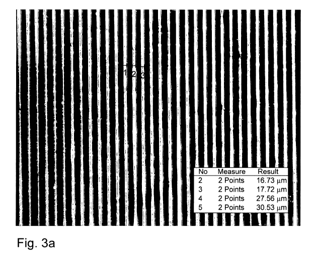
In detail, figure 3a shows a pattern of silver lines comprising a line width
of approximately 17 gm
and spacings there between of approximately 30 gm. Figure 3b shows a pattern
of silver lines
comprising a line width of approximately 40 gm and spacings there between of
approximately 95
gm. Figure 3c shows a pattern of silver lines comprising a line width of
approximately 10 gm and
spacings there between of approximately 40 gm.
It was also possible to print semi-transparent grid patterns by performing two
consecutive printings,
with orientations perpendicular to each other. For example, after the first
print of the silver
CA 02850251 2014-03-27
WO 2013/045424 PCT/EP2012/068835
- 15 -
nanoparticle ink the glass substrate with the pattern was sintered at 350 C
for 10 min. After which,
the substrate was cooled and a second print with an orientation perpendicular
to the first print was
made. The substrate with the print was also sintered at 350 C for another 10
min. This process
resulted in a semi-transparent conductive grid pattern. The microscope images
are given in Fig 4
showing microscope images of the printed grid lines. The grid lines comprise a
12 gm grid with a 25
gm spacing. The sheet resistance was measured to be 0,5 n/sq.. The lines
printed show a thickness
of about 250 nm.
As shown above, the ink formulation according to the invention allows printing
very thin lines, or
patterns, respectively. Consequently, the pattern being formed by the stamp is
appropriately
transferred to the substrate. This shows a very well wetting behavior and
furthermore very well
printing results.
Additionally, the improved wetting behavior of the formulation according to
the invention could be
seen by applying it to a non structured and thus plane poly-(dimethylsiloxane)
surface. In detail,
when having applied the formulation defmed in table 1 onto such a poly-
(dimethylsiloxane) surface,
a contact angle of 33,3 (with a standard deviation of 0,5 ) on the surface
was obtained. This shows
that even hydrophobic surfaces may be applied with the ink formulation
according to the invention
very well leading to an improved wetting behavior.
While the invention has been illustrated and described in detail in the
drawings and foregoing
description, such illustration and description are to be considered
illustrative or exemplary and not
restrictive, the invention is not limited to the disclosed embodiments. Other
variations to the
disclosed embodiments can be understood and effected by those skilled in the
art in practicing the
claimed invention, from a study of the drawings, the disclosure, and the
appended claims. In the
claims, the word "comprising" does not exclude other elements or steps, and
the indefmite article "a"
or "an" does not exclude a plurality. The mere fact that certain measures are
recited in mutually
different dependent claims does not indicate that a combination of these
measures cannot be used to
advantage. Any reference signs in the claims should not be construed as
limiting the scope.