Note: Descriptions are shown in the official language in which they were submitted.
CA 02850947 2014-04-02
WO 2013/059574
PCT/US2012/060993
CLOSED ENTRY DIN JACK AND CONNECTOR
WITH PCB BOARD LOCK
CROSS-REFERENCE TO RELATED APPLICATIONS
[001] This application claims the benefit of U.S. Provisional Patent
Application
Serial No. 61/548,887, filed on October 19, 2011, the disclosure of which is
incorporated
herein in its entirety.
FIELD OF THE INVENTION
[002] The present invention relates generally to electrical connectors.
BACKGROUND
[003] Electrical connectors designed to interface in compliance with
standards
established by the Deutsches Institut fur Normung, a German standards
organization, are
referred to as DIN connectors. FIG. 1 shows a standard DIN 1.0/2.3 connector
100.
The DIN connector 100 includes a DIN plug 102 with a signal pin 104 and a DIN
jack
106 with a mating socket contact 108 axially aligned with the signal pin.
Signal pin 104
and socket contact 108 are disposed within respective hollow, cylindrical
shields 110,
112 that mate telescopically. Problems have been noted when this type of
connector is
miniaturized for use in a large array of connectors. For example, if the
signal pin of a
DIN plug is bent or misaligned even a small amount (e.g., more than 0.006"),
it can brush
by or butt against and damage the DIN jack with resulting signal loss and
reliability
problems.
SUMMARY
[004] Embodiments of a first aspect of the present invention provide a jack
(e.g.,
a DIN jack or other jack) including a tubular socket disposed coaxially within
a hollow
cylindrical shield and a closed entry lead-in that helps prevent damage to the
socket
caused by a bent or misaligned signal pin without adversely affecting the
impedance of
the connector.
[005] In some embodiments of the jack, the lead-in is defined at the distal
end of
a shroud formed of a dielectric material. The shroud has a tubular shroud
portion with
RFEM Docket No.: 3429-214 1
CA 02850947 2014-04-02
WO 2013/059574
PCT/US2012/060993
proximal and distal ends disposed coaxially around the socket and is radially
spaced from
both the socket and the shield. In some embodiments, one or more openings are
formed
laterally through the shroud.
[006] In some embodiments of the jack, the shroud includes a rim extending
radially inward from the distal end of tubular shroud portion and defining a
frustoconical
lead-in coaxially aligned with the socket.
[007] In some embodiments of the jack, the proximal end of the tubular
shroud
portion is coupled with the cylindrical shield or some other part of the
connector body.
[008] In some embodiments of the jack, the shroud includes an annular base
extending radially outward from the proximal end of the hollow tubular shroud
body and
coupled with the connector body.
[009] In some embodiments of the jack, an annular groove is formed along an
inner surface of the cylindrical shield and the annular base of the shroud is
received
within the annular groove.
[0010] In some embodiments of the jack, at least some of the openings in
the
shroud are longitudinally spaced along a length of the tubular shroud portion,
and/or
annularly spaced about a circumference of the tubular shroud body.
[0011] In some embodiments of the jack, the openings are arranged in a
plurality
of longitudinal rows equiangularly spaced about a circumference of the tubular
shroud
body.
[0012] In some embodiments of the jack, the one or more openings are
configured to modify a dielectric constant of the shroud to support 75S2
transmission of
high-speed digital or RF signals.
[0013] In some embodiments, the frustoconical lead-in has a proximal
opening
with a diameter no more than 0.003" larger than the inner diameter of the
tubular socket
and a distal opening larger than the inner diameter of the tubular socket.
[0014] In some embodiments, the shroud is formed of a liquid crystal
polymer.
RFEM Docket No.: 3429-214 2
CA 02850947 2014-04-02
WO 2013/059574
PCT/US2012/060993
[0015] In some embodiments, one or more board locks protrude from the
connector body and include at least one outwardly biased resilient finger with
a rearward-
facing shoulder configured to engage a bottom surface of a printed circuit
board when the
board lock is inserted through a hole in the printed circuit board.
[0016] In some embodiments, a pair of board locks are arranged in
diagonally
opposed relation relative to a longitudinal axis of the jack, alone or in
combination with
one or more mounting pins or posts.
[0017] Embodiments of a second aspect of the present invention provide a
DIN
connector having a jack with a shroud as described above and a mating DIN plug
having
a second connector body with a second hollow cylindrical shield configured to
be
received in the space between the shroud and the first hollow cylindrical
shield and to
make electrical contact with the first shield; and a second contact having a
pin disposed
coaxially within the second hollow cylindrical shield and being configured to
be received
within and make electrical contact with the tubular socket when the plug is
inserted into
the jack.
[0018] Other aspects of the present invention provide a connector jack
with a
shroud as described above, and connectors utilizing such connector jacks.
[0019] The above and other aspects and embodiments are described below
with
reference to the accompanying drawings.
BRIEF DESCRIPTION OF THE DRAWINGS
[0020] The accompanying drawings, which are incorporated herein and form
part
of the specification, illustrate various embodiments of the present invention
and, together
with the description, further serve to explain the principles of the invention
and to enable
a person skilled in the pertinent art to make and use the invention. In the
drawings, like
reference numbers indicate identical or functionally similar elements.
[0021] FIG. 1 is a sectional side view of a prior art DIN connector
showing a DIN
plug partially mated with a DIN jack.
[0022] FIG. 2 is a perspective view of a DIN jack according to an
embodiment of
the invention.
RFEM Docket No.: 3429-214 3
CA 02850947 2014-04-02
WO 2013/059574
PCT/US2012/060993
[0023] FIG. 3 is a sectional side view of the DIN jack shown in FIG. 1
taken
along line 2-2.
[0024] FIG. 4 is a sectional side view of a shroud for use in a DIN jack
according
to an embodiment of the invention.
[0025] FIG. 5 is a bottom view of the DIN jack shown in FIGS. 2 and 3.
[0026] FIG. 6 is a plan view of a printed circuit board configured to
mount the
DIN jack shown in FIGS. 2, 3 and 5.
[0027] FIG. 7 is a sectional side view of a DIN 1.0/2.3 connector with a
DIN jack
according to an embodiment of the invention.
[0028] FIG. 8 is a sectional side view of a right angle DIN jack
according to an
embodiment of the invention for panel mounting on a printed circuit board.
[0029] FIG. 9 is a sectional side view of a DIN to BNC adapter utilizing
a DIN
jack according to an embodiment of the invention.
[0030] FIG. 10 is a sectional side view of a DIN jack for video
applications
according to an embodiment of the invention.
DETAILED DESCRIPTION
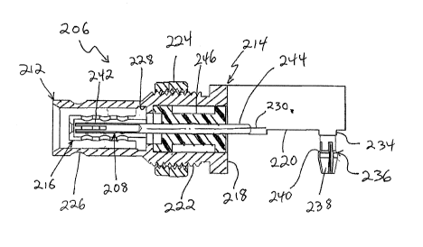
[0031] A DIN jack 206 according to an embodiment of the invention, shown
in
FIGS. 2, 3 and 5, includes a connector body 214, a contact 208, and a shroud
216 that
helps prevent damage to the contact while maintaining RF signal return loss
performance.
In this embodiment, the connector body 214 is configured to allow the DIN jack
to be
edge mounted on a printed circuit board (PCB).
[0032] The connector body 214 is formed of an electrically conductive
material
(e.g., brass) and, as best seen in FIG. 3, includes a distal portion defining
a hollow
cylindrical shield 212 with an open distal end, a proximal portion defining a
proximal
face 218 and one or more downward-facing board mounting surfaces 220
perpendicular
to the proximal face 218, and a threaded portion 222 of hollow cylindrical
configuration
with external screw threads between the proximal and distal portions. A
mounting nut
RFEM Docket No.: 3429-214 4
CA 02850947 2014-04-02
WO 2013/059574
PCT/US2012/060993
224 is preferably provided on the threaded portion 222 of the connector body
for use in
mounting the jack to a panel.
[0033] Referring still to FIG. 3, the cylindrical shield includes a first
annular
groove 226 formed about an outer circumference of the shield near the distal
end, and a
second annular groove 228 formed about an inner circumference of the shield
near the
proximal end. The board mounting surfaces 220 are preferably planar and
oriented
parallel to and in alignment with the central longitudinal axis 230 of the
cylindrical shield
to align the center of the shield with the edge of a PCB when the mounting
surfaces 220
abut the top of the PCB. Referring to FIGS. 3 and 5, the board mounting
surfaces 220 are
defined along respective bottom edges of two parallel arms 232a and 232b
oriented
parallel to the longitudinal axis 230 of the connector and laterally spaced
apart. Two
posts 234 are shown extending downwardly from the bottom edge of each arm, and
the
planar mounting surfaces 220 are disposed between the posts 234.
[0034] A board lock 236 extends downwardly from one of the two posts 234
on
each arm. Preferably, the board locks 236 are located on alternate posts so
that, when
viewed from the bottom as shown in FIG. 5, the board locks 236 are arranged in
diagonally opposed relation (e.g., longitudinally and laterally spaced from
one another).
Each board lock includes a plurality of outwardly biased fingers or tines 238
combining
to form a generally frustoconical insert with upwardly facing shoulders 240
configured to
abut a bottom of the PCB when the board lock is inserted through a hole in the
PCB and
the mounting surfaces 220 abut the top of the PCB. The board locks 236 can be
formed
of any conductive material with suitable elasticity, e.g., phosphor bronze per
ASTM
8139.
[0035] In the embodiment shown, the posts 234 without board locks are
also
arranged in diagonally opposed relation. In an embodiment, a post without a
board lock
on one arm is longitudinally aligned with a board lock on the other arm. It
has been
found that this arrangement helps meet spatial requirements by facilitating
proper
positioning and alignment of the connector on the PCB and by securely holding
the jack
in place during the soldering process.
RFEM Docket No.: 3429-214 5
CA 02850947 2014-04-02
WO 2013/059574
PCT/US2012/060993
[0036] As best seen in FIG. 3, the contact includes a tubular socket 242
with an
open distal end disposed coaxially within the hollow cylindrical shield 212.
The tubular
socket 242 is of much smaller diameter than the shield 212, so the socket and
shield are
separated by an annular gap. In an embodiment, the tubular socket 242 has an
outer
diameter of 0.03 inches and an inner diameter of 0.02 inches, and the hollow
cylindrical
shield 212 has an inner diameter of 0.11 inches. A solder tail 244, preferably
having the
same outer diameter as the tubular socket 242, extends longitudinally from the
tubular
socket 242 in a proximal direction to protrude slightly from the proximal face
218 of the
housing between the parallel arms at the proximal end of the housing. The
contact 208
can be formed of any suitable electrically conductive material, e.g., a copper
alloy, and is
held in place by a sleeve 246 formed of an insulating material, e.g., PTFE
(Teflon),
disposed within the connector body 214. In the embodiment shown, a lower edge
of the
solder tail 244 is slightly below the plane defined by the mounting surfaces
220. In a
preferred embodiment, a central longitudinal axis 230 of the solder tail 244
is coplanar
with the mounting surfaces 220.
[0037] Referring now to FIGS. 3 and 4, the shroud 216 is formed of a
dielectric
material and includes a tubular shroud portion 248 with proximal and distal
ends, and an
annular base 250 extending radially outward from the proximal end of the
tubular shroud
portion 248. An outer edge of the annular base 250 is received within the
annular groove
228 formed along the inner circumference of the cylindrical shield. The
tubular shroud
portion 248 extends coaxially around the contact socket 208 within the annular
gap
between the socket and the shield and is held in radially spaced relation to
the socket and
the shield so as to define first and second radial gaps therebetween. In an
embodiment,
the first radial gap (between the shroud 216 and the socket contact 208) is
0.005-0.015
inches, or preferably 0.01 inches, and the second radial gap (between the
shroud 216 and
the shield 212) is 0.015-0.025 inches, or preferably 0.02 inches.
[0038] In the embodiment shown, the shroud 216 includes a rim 252
extending
radially inward from the distal end of tubular shroud portion 248 and defining
a
frustoconical lead-in 254 coaxially aligned with the socket. In an embodiment,
the
diameter of the lead-in decreases from 0.036 inches to 0.022 inches in the
proximal
direction, and the included angle 0 of the lead-in is 90 degrees. In the case
of the
RFEM Docket No.: 3429-214 6
CA 02850947 2014-04-02
WO 2013/059574
PCT/US2012/060993
foregoing embodiment, the shroud 216 allows the socket 242 to be used with
pins that are
axially misaligned as much as 0.018 inches more than a standard connector
socket. The
lead-in terminates proximally in a straight through-hole having a diameter
equal to the
proximal diameter of the frustoconical opening, preferably 0.022 inches, which
is only
slightly larger than the inner diameter of the tubular socket 242 (preferably
0.02 inches).
By interposing the lead-in between the socket and a mating plug with pin
contact, the
shroud 216 helps eliminate damage caused by a misaligned pin contact butting
against or
sliding past the socket.
[0039] Referring specifically to FIG. 4, it can be seen that the tubular
shroud
portion 248 has a wall thickness and a plurality of openings 256 that are
formed laterally
(i.e., perpendicular to the longitudinal axis 230) through the thickness of
the wall. The
wall thickness and number, size and location of the openings 256 are selected
to produce
a desired characteristic impedance. In some embodiments, (as illustrated by
the
dimensions shown in FIG. 4) the wall thickness of the tubular shroud portion
248 is about
0.01 inches (e.g., as shown in FIG. 4 the outer diameter (od) is about 0.073
inches and the
inner diameter (id) is about 0.053 inches; as also shown the length (L) of the
tubular
shroud portion is about 0.175 inches in some embodiments, in other embodiments
the
length is less than 0.5 inches). In some embodiments, the wall thickness of
portion 248
ranges from 0.01 inches to 0.1 inches. In the embodiment shown, twelve
circular
openings 256 are formed through the shroud 216 in four longitudinal rows
spaced
equiangularly about the circumference of the shroud 216. In a preferred
embodiment,
each row includes three circular holes of 0.031 inch diameter spaced 0.05 inch
apart
center-to-center. In a preferred embodiment, counterpart openings 256 in
adjacent rows
are longitudinally aligned. The shroud 216 can be formed of any dielectric
material that
meets the thermal and mechanical requirements of the application. In
particular, the
shroud material is preferably hard enough for the lead-in to guide a
misaligned pin to the
socket without breaking and for the tubular shroud portion to resist bending
when a
misaligned pin slides against it. In addition, the shroud material preferably
supports 75S2
transmission of high-speed digital (e.g., up to 6 Gbps) and radio frequency
(RF) signals
while maintaining RF signal return performance better than -25 dB to 5 GHz. In
an
embodiment, the invention supports up to 6 GHz and performance requirements
per
RFEM Docket No.: 3429-214 7
CA 02850947 2014-04-02
WO 2013/059574
PCT/US2012/060993
SMPTE-424 3 Gbit/s 3G-SDI broadcast signaling. In a preferred embodiment, the
shroud 216 is formed of a dielectric material having a heat deflection
temperature greater
than 260 C (more preferably, 280 C) and a compression strength of at least
15 lbs
(measured perpendicular to the longitudinal axis of the tubular shroud
portion). In an
embodiment, the shroud 216 is formed of a polyethermide, such as Ultem 1000
(unfilled).
In a preferred embodiment, the shroud 216 is formed of a liquid crystal
polymer (LCP);
and, more preferably, a glass-filled LCP, such as Zenite 6130LX BK010.
[0040] FIG. 6 shows an edge portion of a PCB 258 with two pairs of
diagonally
opposed mounting holes 260 and 262 to receive the board locks 236 and
alignment posts
234, respectively. The mounting holes are spaced from the edge 264 of the PCB
so that
the proximal face 218 of the connector body 214 abuts the edge of the PCB when
the
board locks 236 and posts 234 are inserted through the mounting holes. The PCB
also
includes a small longitudinal trough 266 extending proximally from the edge of
the PCB
to receive the solder tail 244 when the DIN jack is mounted on the edge of the
PCB. In
an embodiment, the mounting holes are plated through holes. In an embodiment,
the
PCB is 0.063 inches thick. In an embodiment, at least some, and preferably
all, of the
mounting holes are plated through-holes.
[0041] In use, DIN jack 206 can be edge-mounted on a PCB by aligning the
board locks 236 and posts 234 on the connector body 214 with corresponding
holes in the
PCB and pressing the jack and the PCB towards one another. As the jack and the
PCB
are pressed together, the tines of the board locks 236 will be deflected
radially inwardly
by the walls of the through holes and will spring radially outward once free
from the hole
to cause the PCB to be sandwiched between the bottom edges of the connector
body 214
and the upwardly facing shoulders of the board locks 236. The spacing of the
holes from
the edge of the PCB also ensures that the proximal face 218 of the connector
body 214 is
closely adjacent to or in contact with the edge of the PCB, so that in
combination with the
board locks 236 and posts 234, the jack is held firmly in place and unable to
move
excessively in any direction. Once properly positioned, the solder tail 244 is
preferably
disposed within the trough formed at the edge of the board, between the
connector arms,
accessible for soldering. The jack 206 is then soldered to the board. The
board lock
RFEM Docket No.: 3429-214 8
CA 02850947 2014-04-02
WO 2013/059574
PCT/US2012/060993
feature also improves the manufacturing process by securing the jack so that
there is no
need to fixture a single jack or an array of jacks to the PCB during wave or
reflow
soldering. The board locks 236 also reduce manufacturing time by increasing
the
efficiency of placement and holding the jack 206 securely to the circuit board
while the
PCB is handled and soldered. In an embodiment, the shroud is formed of a
material with
sufficient heat deflection temperature to avoid becoming misaligned during the
soldering
process.
[0042] It will be appreciated that the DIN jack 206 of the present
invention can
interface with a standard DIN plug 102 as shown in FIG. 7. The pin 104 of the
DIN plug
102 is received within the tubular socket 242, and the cylindrical shield 110
of the plug
is received within the gap between the shroud 216 and the cylindrical shield
112 of the
jack.
[0043] A right angle DIN jack 306 according to another embodiment of the
invention, for panel mounting on a printed circuit board, is shown in FIG. 8.
The DIN
jack 300 includes a hollow cylindrical shield 212, a tubular socket 242, and a
shroud 216
like the DIN jack 206 shown in FIGS. 2-5; however, the connector body 314 and
solder
tail 344 are configured to facilitate panel mounting on a PCB. Specifically,
the connector
body 314 includes a cube-like proximal portion defining a single board
mounting surface
320 laterally spaced from the central longitudinal axis 230 of the shield so
that the jack
interface (and the nut) is elevated from the surface of the PCB. In this
embodiment, the
solder tail 344 extends from the proximal face 318 of the connector body and
bends 90
degrees downward towards to the PCB. A second insulator 368 holds the solder
tail 344
in position between the board locks 236 and the posts 234. This DIN jack can
be surface
mounted on a PCB having mounting holes like the ones shown in FIG. 6, but with
the
addition of a central plated through-hole for the solder tail.
[0044] In another embodiment of the present invention, shown in FIG. 9, a
DIN
to BNC adapter 406 is provided. The adapter 406 includes a hollow cylindrical
shield
212, a tubular socket 242, and a shroud 216 like the DIN jack 206 shown in
FIGS. 2-5;
however, proximal ends of the connector body 414 and the contact 408 are
configured to
define the shield 470 and socket 472 of a BNC jack.
RFEM Docket No.: 3429-214 9
CA 02850947 2014-04-02
WO 2013/059574
PCT/US2012/060993
[0045] In yet another embodiment, shown in FIG. 10, a DIN video jack 506
is
provided. The DIN video jack 506 includes a hollow cylindrical shield 212, a
tubular
socket 242, and a shroud 216 like the DIN jack 206 shown in FIGS. 2-4;
however,
proximal ends of the connector body 514 and the contact 508 are configured to
interface
with high definition video equipment 574.
[0046] While various embodiments of the present invention have been
described
above, it should be understood that they have been presented by way of example
only,
and not limitation. For example, while the shroud is shown as an integral, one-
piece unit,
it will be appreciated that the shroud can be made-up of multiple pieces that
are bonded,
fused, or otherwise connected together to form an integral unit. Also, while
certain
adapters are shown for converting between DIN and other interfaces, it will be
appreciated that other adapters can be made using the DIN jack of the present
invention.
For example, the DIN jack can be used in a DIN jack to BNC plug. Further,
while
specific sheath openings are disclosed herein, it will be appreciated that
other shapes,
sizes, and/or numbers of openings can be used. Also, the arrangement of the
openings
can be modified. For example, the number of longitudinal rows of openings may
be
greater or fewer than shown, and the openings in adjacent rows may be
longitudinally
aligned as shown, or staggered. It will also be appreciated that, although the
invention
has been described with reference to the DIN 1.0/2.3 interface, the present
invention may
be embodied in other types of jacks and connector interfaces used in high-
speed digital
and RF applications. Additionally, the board lock feature may be used on a
jack, as
shown, or a plug. Thus, the breadth and scope of the present invention should
not be
limited by any of the above-described exemplary embodiments.
RFEM Docket No.: 3429-214 10