Note: Descriptions are shown in the official language in which they were submitted.
CA 02851011 2014-05-08
266983
DEVICE AND METHOD TO BREAK THE CURRENT IN POWER TRANSMISSION
OR DISTRIBUTION SYSTEM
BACKGROUND
100011 Embodiments of the invention relate generally to devices and methods
to
break current, and in particular, to direct current (DC) circuit breakers
applied in high-
voltage direct current (HVDC) systems, medium-voltage direct current (MVDC)
power
transmission or distribution systems, or the like.
[0002] In recent years, the interest in HVDC or MVDC systems has been
revived.
In those HVDC or MVDC systems, DC circuit breakers are necessary to make the
HVDC
or MVDC systems more flexible and reliable for many applications such as multi-
terminal HVDC grids, MVDC power distribution for subsea electrification, and
marine
MVDC power transmission and so on. The DC circuit breakers need to be
developed and
validated at full scale to operate a multi-terminal HVDC or MVDC grid
protection for
fast interruption time and low loss.
[0003] Existing mechanical DC circuit breakers are capable of interrupting
HVDC
or MVDC currents within several tens of milliseconds, but are too slow to
fulfill the
requirements of reliable HVDC or MVDC grids. For fulfilling the high speed
requirements, several approaches have been investigated. For example, a DC
circuit
breaker consists of silicon insulated gate bipolar transistors (IGBTs), which
are controlled
to interrupt HVDC or MVDC currents within a few milliseconds. However, the
traditional silicon IGBTs may consume lots of energy during the energy
transmission
process, which decreases efficiency. Furthermore, due to the silicon IGBTs
generating a
lot of heat, heat sinks need to be arranged on the silicon IGBTs. This
requires additional
space and increases the weight of the HVDC or MVDC grids, which in turn
reduces their
power density and performance.
1
CA 02851011 2014-05-08
266983
[0004] For these and other reasons, there is a need for providing a new DC
circuit
breaker at least having capabilities of low conduction loss and faster
switching speed.
BRIEF DESCRIPTION
[0005] In accordance with an embodiment of the invention, a direct current
(DC)
circuit breaker having capabilities of low conduction loss and faster
switching speed for
power transmission or distribution system is provided. The DC circuit breaker
includes a
current sensor for sensing current of a system, a controller, a physical
switch, and
multiple switch modules. The multiple switch modules are electrically coupled
to the
current sensor and the physical switch in series. Each switch module includes
multiple
base elements electrically coupled in parallel. Each base element includes a
first silicon
carbide (SiC) metal-oxide-semiconductor field-effect transistor (MOSFET) and a
second
SiC MOSFET electrically coupled in an opposite series connection mode. The
first and
second SiC MOSFETs are configured in a synchronous rectification mode by
channel
reverse conduction control. The controller controls the multiple switch
modules to
connect current in the system, and break current of the multiple switch
modules
according to sensed current signals from the current sensor.
[0006] In accordance with an embodiment of the invention, a current
connecting
method for the DC circuit breaker is provided. The current connecting method
includes
turning on the physical switch at a first time point; turning on the first SiC
MOSFET of
each base element at a second time point after a predetermined time interval
from the first
time point; and turning on the second SiC MOSFET of each base element at a
third time
point after a predetermined time interval from the second time point. The
current
direction is from the first SiC MOSFET to the second SiC MOSFET of each base
element.
100071 In accordance with an embodiment of the invention, a current
breaking
method for the DC circuit breaker is provided. The current breaking method
includes
turning off the first SiC MOSFET of each base element at a first time point;
turning off
the physical switch at a second time point after a predetermined time interval
from the
2
CA 02851011 2014-05-08
266983
first time point; and turning off the second SiC MOSFET of each base element
at a third
time point after a predetermined time interval from the second time point. The
current
direction is from the first SiC MOSFET to the second SiC MOSFET of each base
element.
DRAWINGS
[0008] These and other features, aspects, and advantages of the present
invention
will become better understood when the following detailed description is read
with
reference to the accompanying drawings in which like characters represent like
parts
throughout the drawings, wherein:
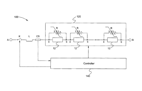
[0009] FIG. 1 is a block diagram of a DC circuit breaker according to one
embodiment.
[0010] FIG. 2 is a circuit diagram of a switch module of the DC circuit
breaker of
FIG. 1 according to one embodiment.
[0011] FIG. 3 is a flowchart of a DC current connecting method for the
switch
modules and a mechanical switch of the DC circuit breaker of FIG. 1 according
to one
embodiment.
[0012] FIG. 4 is a time sequence diagram for showing three switch commands
of
the DC circuit breaker of FIG. 1 during a current connecting process.
[0013] FIG. 5 is a schematic view for showing current flowing statuses in a
base
element of a switch module and the mechanical switch of the DC circuit breaker
of FIG.
1 in four different statuses during the current connecting process.
[0014] FIG. 6 is a flowchart of a DC current breaking method for the switch
modules and the mechanical switch of the DC circuit breaker of FIG. 1
according to one
embodiment.
3
CA 02851011 2014-05-08
266983
[0015] FIG. 7 is a time sequence diagram for showing three switch commands
of
the DC circuit breaker of FIG. 1 both during a current connecting process and
a current
breaking process.
[0016] FIG. 8 is a schematic view for showing current flowing statuses in a
base
element of a switch module and the mechanical switch of the DC circuit breaker
of FIG.
1 in four different statuses during the current breaking process.
DETAILED DESCRIPTION
[0017] Embodiments of the invention relate to a direct current (DC) circuit
breaker
for power transmission or distribution system. The DC circuit breaker includes
a current
sensor for sensing current of a system, a controller, a physical switch, and
multiple switch
modules. The multiple switch modules are electrically coupled to the current
sensor and
the physical switch in series. Each switch module includes multiple base
elements
electrically coupled in parallel. Each base element includes a first silicon
carbide (SiC)
metal-oxide-semiconductor field-effect transistor (MOSFET) and a second SiC
MOSFET
electrically coupled in an opposite series connection mode. The first and
second SiC
MOSFETs are configured in a synchronous rectification mode by channel reverse
conduction control. The controller controls the multiple switch modules to
connect
current in the system, and break current of the multiple switch modules
according to
sensed current signals from the current sensor.
[0018] Unless defined otherwise, technical and scientific terms used herein
have the
same meaning as is commonly understood by one of ordinary skill in the art to
which this
invention belongs. The terms "first", "second", and the like, as used herein
do not denote
any order, quantity, or importance, but rather are used to distinguish one
element from
another. Also, the terms "a" and "an" do not denote a limitation of quantity,
but rather
denote the presence of at least one of the referenced items, and terms such as
"front",
"back", "bottom", and/or "top", unless otherwise noted, are merely used for
convenience
of description, and are not limited to any one position or spatial
orientation. Moreover,
4
CA 02851011 2014-05-08
266983
the terms "coupled" and "connected" are not intended to distinguish between a
direct or
indirect coupling/connection between two components. Rather, such components
may be
directly or indirectly coupled/connected unless otherwise indicated.
[0019] Referring to FIG. 1, a block diagram of a DC circuit breaker 100
according
to one embodiment is shown. The DC circuit breaker 100 can be applied in any
power
transmission or distribution systems, such as high-voltage direct current
(HVDC) systems,
medium-voltage direct current (MVDC) systems, etc., to break current when the
current
flowing therein is not within a predetermined range or when the power
transmission
systems fall into some situations which need to quickly cut the current off
[0020] In this illustrated embodiment, the DC circuit breaker 100 includes
two
terminals 'A' and 'B', a mechanical switch K, a current limiter L, a current
sensor CS, a
current breaking unit 120, and a controller 140. In one embodiment, the
current limiter L
is an inductor. The controller 140 may be any type of programmable devices,
such as a
micro-controller, a micro control unit (MCU), a digital signal processor
(DSP), etc.
[0021] The two terminals 'A' and '13' are used to electrically couple the
DC circuit
breaker 100 into a current transmission line of a power transmission system
(not shown).
The current sensor CS is used to sense current flowing through the DC circuit
breaker
100. The controller 140 is used to receive sensed current signals from the
current sensor
CS and control the mechanical switch K and the current breaking unit 120
according to
the sensed current signals. In a normal working status, the controller 140
switches the
mechanical switch K and the current breaking unit 120 on to ensure the current
can be
transmitted through the DC circuit breaker 100. In an abnormal working status,
for
example when the sensed current signal is greater than a predetermined maximum
value,
such as 2kA, the controller 140 switches the mechanical switch K and the
current
breaking unit 120 off to interrupt the current flowing through the DC circuit
breaker 100.
In general, the current breaking unit 120 is used to provide a fast current
interruption and
the mechanical switch K is used to provide a physical current interruption. In
some
embodiments, the mechanical switch K also can be controlled manually.
CA 02851011 2014-05-08
266983
[0022] The current breaking unit 120 includes at least one switch module 12
electrically coupled in series. The number of the series-connected switch
modules 12 is
determined according to the current value flowing through the DC circuit
breaker 100.
When the current flowing through the DC circuit breaker 100 is getting
greater, the
number of the series-connected switch modules 12 is getting greater
accordingly, and
vice versa. Each switch module 12 further electrically couples to a non-linear
resister R
in parallel. The non-linear resister R can help balance the voltage sharing,
as well as
absorb the fault current breaking energy. Every switch module 12 has a similar
function;
therefore only one switch module 12 will be described in detail in the
following
paragraphs.
[0023] Referring to FIG. 2, a circuit diagram of a switch module 12
according to
one embodiment is shown. The switch module 12 may include a plurality of base
elements 122 electrically coupled in parallel. The number of the parallel-
connected base
elements 122 is also determined according to the current value flowing through
the DC
circuit breaker 100. The illustrated embodiment shows an exemplary embodiment
which
includes three parallel-connected base elements 122. Every base element 122
has a
similar function; therefore only one base element 122 will be described in
detail in the
following paragraphs.
[0024] In this illustrated embodiment, the base element 122 includes a
first silicon
carbide (SiC) metal-oxide-semiconductor field-effect transistor (MOSFET) Q1
and a
second SiC MOSFET Q2 electrically coupled in an opposite series connection
mode.
The first SiC MOSFET Q1 further includes a free-wheeling diode Dl. The second
SiC
MOSFET Q2 further includes a free-wheeling diode D2.
[0025] In one embodiment, the drain terminal of the first SiC MOSFET Q1 is
connected to a first terminal 'a', the source terminal of the first SiC MOSFET
Q1 is
connected to the source terminal of the second SiC MOSFET Q2, the gate
terminal of the
first SiC MOSFET Q1 is used to receive control commands from the controller
140, the
cathode of the diode D1 is connected to the drain terminal of the first SiC
MOSFET Q1,
6
CA 02851011 2014-05-08
266983
the anode of the diode D1 is connected to the source terminal of the first SiC
MOSFET
Ql. The drain terminal of the second SiC MOSFET Q2 is connected to a second
terminal
`1)', the gate terminal of the second SiC MOSFET Q2 is used to receive control
commands from the controller 140, the cathode of the diode D2 is connected to
the drain
terminal of the second SiC MOSFET Q2, the anode of the diode D2 is connected
to the
source terminal of the second SiC MOSFET Q2. In other embodiments, there may
be
more first SiC MOSFETs Q1 connected in series to handle a greater current, or
there may
be more second SiC MOSFETs Q2 connected in series to handle a greater current.
The
number of the first SiC MOSFETs Q1 and the number of the second SiC MOSFET Q2
may vary according to actual current requirements. The diode D1 and D2 can
either be
SiC MOSFET parasitical diodes or external paralleled diodes.
[0026] During a startup process of the DC circuit breaker 100, which means
to
ensure the current can be flowed through the DC circuit breaker 100, the
controller 140
outputs control commands to the mechanical switch K and the switch modules 12
according to predetermined programs. The controller 140 outputs those control
commands according to a startup signal from the power transmission or
distribution
system. A flowchart of a DC current connecting method 30 for the switch
modules 12
and the mechanical switch K is shown in FIG. 3 as an exemplary embodiment.
Herein,
the current direction is from the terminal 'A' to 13'. The DC current
connecting method
30 includes the following steps.
[0027] In step 31, the mechanical switch K is turned on at a first time
point Ti
according to a control command SK shown as a command wave 41 in FIG. 4. This
mechanical switch K is used to provide a physical connection between the two
terminals
'A' and 13'. In other embodiments, the mechanical switch K may be other types
of
physical switches. After turning on the mechanical switch K, a physical
connection
between the two terminals 'A' and '13' is finished firstly. Referring to FIG.
5, an initial
status 51 is shown, and a status 52 of the step 31 is shown. In the initial
status 51, the
mechanical switch K and the switch modules 12 are opened. In this status 52,
the
7
CA 02851011 2014-05-08
266983
mechanical switch K is turned on, but due to the MOSFETs Q1 and Q2 are not
turned on,
there is no current flowing through the DC circuit breaker 100 yet.
[0028] In step 32, after a predetermined time interval from the first time
point Ti,
such as after about 1 microseconds to 1000 microseconds, all of the first SiC
MOSFETs
Q1 are turned on at a second time point T2 according to a control command SQ1
shown as
a command wave 42 in FIG. 4. Referring to FIG. 5, a status 53 of the step 32
is shown.
In this status 53, the mechanical switch K is turned on, the first SiC MOSFETs
Q1 are
turned on as well, but the second SiC MOSFETs Q2 are not turned on yet.
Therefore, the
current will pass through the mechanical switch K, pass through the first SiC
MOSFETs
Q1 from the drain terminal to the source terminal thereof, and pass through
the diode D2
of the second SiC MOSFETs Q2 (see arrows from 'A' to 'EV). Even though the
current
can pass through the DC circuit breaker 100, the power loss may be large in
the second
SiC MOSFETs Q2 because of the diode D2 may consume power greater. However,
compared with the conventional Si IGBT configuration, this SiC MOSFET
configuration
only consumes about 0.2-0.5 times power loss. Furthermore, the switch response
speed
of the SiC MOSFEF configuration is faster about 5-10 times compared with the
conventional Si IGBT configuration.
[0029] In step 33, after a predetermined time interval from the second time
point T2,
such as after about 1 microseconds to 1000 microseconds, all of the second SiC
MOSFETs Q2 are turned on at a third time point T3 according to a control
command SQ2
shown as a command wave 43 in FIG. 4. Referring to FIG. 5, a status 54 of the
step 33 is
shown. In this status 54, the mechanical switch K is turned on, the first SiC
MOSFETs
Q1 are turned on, and the second SiC MOSFETs Q2 are turned on as well.
Therefore, the
current will pass through the mechanical switch K, pass through the first SiC
MOSFETs
Q1 from the drain terminal to the source terminal thereof, and pass through
the second
SiC MOSFETs Q2 from the source terminal to the drain terminal thereof (see
arrows
from 'A' to 'EV). This is due to the SiC MOSFETs having synchronous
rectification (SR)
mode by a channel reverse conduction control, which can operate current
through the SiC
8
CA 02851011 2014-05-08
266983
MOSFETs along a less loss channel, which may further reduce about 17% power
loss
after performing this step 33.
[0030] In other words, with the positive gate drive signals to the gate
terminals of
the SiC MOSFETs' Q1 and Q2, each of the SiC MOSFETs Q1 and Q2 can be a
reversed
channel conduction from the drain terminal to the source terminal or from the
source
terminal to the drain terminal but not passing through the diodes D1 and D2,
which can
make the current pass through the less-loss device channel. Therefore,
compared with the
conventional DC circuit breakers, the SiC MOSFETs Q1 and Q2 will consume less
energy during the conduction process. Thus, by using the SiC MOSFETs Q 1 and
Q2
instead of the conventional semiconductor switches, such as silicon IGBTs, the
energy
transfer efficiency is increased. Furthermore, because the SiC MOSFETs Q1 and
Q2
consume less energy, the heat generated by the SiC MOSFETs Q1 and Q2 is less
than the
heat generated by the conventional semiconductor switches. Furthermore, the
SiC
MOSFET can handle higher operation temperature (such as bigger than 175
degrees
Celsius). Therefore, the number or volume of the heat sinks (not shown)
arranged on the
SiC MOSFETs Q1 and Q2 may be less than the number or volume of the heat sinks
that
are required for a conventional semiconductor switches.
[0031] When the current direction is from the terminal 'B' to 'A', the step
32 and
step 33 is reversed. In other words, the second SiC MOSFETs Q2 are turned on
first and
then the first SiC MOSFETs Q1 are turned on.
[0032] During a current breaking process of the DC circuit breaker 100,
which
means to interrupt current flowing through the DC circuit breaker 100, the
controller 140
outputs control commands to the mechanical switch K and the switch modules 12
according to predetermined programs. The controller 140 outputs those control
commands according to the current sensing signals sensed by the current sensor
CS, for
example when a current sensing signal is greater than a predetermined value. A
flowchart of a DC current breaking method 60 for the switch modules 12 and the
mechanical switch K is shown in FIG. 6 as an exemplary embodiment. Herein, the
9
CA 02851011 2014-05-08
266983
current direction is from the terminal 'A' to 'W. The DC current breaking
method 60
includes the following steps.
[0033] In step 61, the first SiC MOSFETs Q1 is turned off at a fourth time
point T4
according to the control command SQ1 shown as a command wave 72 in FIG. 7.
Referring to FIG. 8, a normal working status 81 (same as the status 54 shown
in FIG. 5)
is shown, and a status 82 of the step 61 is shown. In this status 82, the SiC
MOSFETs Q1
are turned off, therefore the current is interrupted immediately. Due to the
switch time of
the SiC MOSFET is very short, may be take only a few milliseconds, which can
satisfy
the quick switch requirement of the power transmission or distribution system.
[0034] In step 62, after a predetermined time interval from the fourth time
point T4,
such as after about 1 microseconds to 1000 microseconds, the mechanical switch
K is
turned off at a fifth time point T5 according to the control command SK shown
in FIG. 7.
After the mechanical switch K is turned off, the physical connection between
the two
terminals 'A' and `I3' is cut off. Referring to FIG. 8, a status 83 of the
step 62 is shown.
In this status 52, the mechanical switch K is turned off, and the first
MOSFETs Q1 are
turned off
[0035] In step 63, after a predetermined time interval from the fifth time
point T5,
such as after about 1 microseconds to 1000 microseconds, all of the second SiC
MOSFETs Q2 are turned off at a sixth time point T6 according to the control
command
SQ2 showing in FIG. 7. Referring to FIG. 8, a status 84 of the step 63 is
shown. In this
status 84, the mechanical switch K is turned off, the first SiC MOSFETs Q1 is
turned off,
and the second SiC MOSFETs Q2 is turned off as well. Therefore, the current
connecting points are all cut off finally and back to the initial status 51.
When the current
fault is gone, the power transmission system can be recovered according to the
control
performed by the DC current connecting method 30.
CA 02851011 2014-05-08
266983
[0036] When the current direction is from the terminal '13' to 'A', the
step 61 and
step 63 is reversed. In other words, the second SiC MOSFETs Q2 is turned off
firstly and
then the first SiC MOSFETs Q1 is turned off after the mechanical switch K is
turned off.
[0037] While the invention has been described with reference to exemplary
embodiments, it will be understood by those skilled in the art that various
changes may
be made and equivalents may be substituted for elements thereof without
departing from
the scope of the invention. In addition, many modifications may be made to
adapt a
particular situation or material to the teachings of the invention without
departing from
the essential scope thereof. Therefore, it is intended that the invention not
be limited to
the particular embodiment disclosed as the best mode contemplated for carrying
out this
invention, but that the invention will include all embodiments falling within
the scope of
the appended claims.
[0038] It is to be understood that not necessarily all such objects or
advantages
described above may be achieved in accordance with any particular embodiment.
Thus,
for example, those skilled in the art will recognize that the systems and
techniques
described herein may be embodied or carried out in a manner that achieves or
optimizes
one advantage or group of advantages as taught herein without necessarily
achieving
other objects or advantages as may be taught or suggested herein.
11