Note: Descriptions are shown in the official language in which they were submitted.
CA 02851837 2014-05-13
SYSTEMS AND METHODS FOR ACQUIRING A RECEIVED DATA SIGNAL IN A CLOCK
AND DATA RECOVERY CIRCUIT
BACKGROUND
Technical Field
[0001] The embodiments described herein relate to clock and data recovery
circuits.
Related Art
[0002] In, e.g., communication applications, processing circuitry often
processes data in a
parallel manner, but the data are often communicated between points serially.
Data may be
transmitted serially over channels such as circuit board traces, backplanes,
or fiber optic cables. A
transmitter for serial communication can transmit data in a data signal with
clocking information
signaled implicitly by the timing of transitions in the data signal. A
receiver recovers both the
transmitted data and a corresponding clock signal. Circuitry in the receiver
performing such
operations is often termed a clock and data recovery circuit or more commonly
a CDR.
[0003] Many clock and data recovery circuits operate using critical analog or
quasi-analog
circuits such as voltage-controlled oscillators, phase-frequency detectors,
charge pumps, and
filters. Such circuits can be difficult to develop and manufacture.
Additionally, desires for higher
speeds and reduced cost and power increase the difficulties in developing and
manufacturing
CDRs.
[0004] One problem with conventional CDRs is the difficulty of matching the
receiver operation
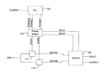
to that of the transmitter. The problem arises due to the fact that the clock
circuitry in the
transmitter and receiver will not operate at the exact same frequency due to
manufacturing
tolerances. Moreover, each of the clocks in the transmitter and receiver will
drift over time at
different rates. Accordingly, it is very difficult to keep the operation of
the receiver and the
- 1 -
CA 02851837 2014-05-13
transmitter locked to each other and some active operation is typically needed
to ensure that the
two remain locked.
[0005] A conventional technique is to over sample the data signal received in
the receiver using
multiple phases of the receiver clock. This allows control circuitry in the
receiver to "map" the
received data signal and determine the optimum point, and corresponding phase
at which to
sample the received signal. It will be understood that conventionally, at
least 3 phases per bit
must be used in such an over sampling scheme; however, this increases the
complexity, size, and
cost of the receiver.
SUMMARY
[0006] Systems and methods for detecting recovering a data and clock signal in
a communication
system are described herein.
[0007] in one aspect, a data recovery circuit, comprises a first flip-flop
configured to store values
of a serial input signal at times signaled by a first sample signal; a second
flip-flop configured to
store values of the serial input signal at times signaled by a second sample
signal; a phase select
module configured to produce the first sample signal and the second sample
signal, the first
sample signal and the second sample signal oscillating at a frequency matching
an expected data
rate of the serial input signal and having phases with selected offsets; and a
control module
configured to produce an output data signal from only the values from the
first flip-flop and the
second flip-flop, and to control the phase select module to produce the first
sample signal and the
second sample signal to recover data from the serial input signal.
[0008] In another aspect, a data recovery circuit, comprises a first flip-flop
configured to produce
a first data sample signal by storing values of a serial input signal at edges
of a first sample signal; a
second flip-flop configured to produce a second data sample signal by storing
values of the serial
- 2 -
CA 02851837 2014-05-13
input signal at edges of a second sample signal; a phase select module
configured to produce the
first sample signal by selecting one of plurality of phase signals according
to a first phase control
signal and produce the second sample signal by selecting one of the plurality
of phase signals
according to a second phase control signal, each of the plurality of phase
signals offset in phase
and oscillating at a frequency corresponding to the data rate of the serial
input signal; an
accumulate module configured to accumulate counts of miscompares between
values of the first
data sample signal and the second data sample signal; a data selector
configured to produce an
output data signal by selecting the first data sample signal or the second
data sample signal
according to a data select control signal; and a control module configured to
produce the first
phase control signal, the second phase control signal, and the data select
control signal using the
accumulated counts of miscompares so that the output data signal signals data
recovered from the
serial input signal, wherein only the first flip-flop and the second flip-flop
store values of the serial
input signal.
[0009] Other features and advantages of the present invention should be
apparent from the
following description which illustrates, by way of example, aspects of the
invention.
BRIEF DESCRIPTION OF THE DRAWINGS
[0010] The details of the present invention, both as to its structure and
operation, may be
gleaned in part by study of the accompanying drawings, in which like reference
numerals refer to
like parts, and in which:
[0011] FIG. 1 is a block diagram of a clock and data recovery circuit in
accordance with aspects of
the invention;
[0012] FIG. 2 is a timing diagram illustrating operation of a clock and data
recovery circuit in
accordance with aspects of the invention;
- 3 -
CA 02851837 2014-05-13
[0013] FIG. 3 is a block diagram of a clock and data recovery circuit in
accordance with aspects of
the invention;
[0014] FIG. 4 is a block diagram of a communication system in accordance with
aspects of the
invention;
[0015] FIG. 5 is a block diagram illustrating an example circuit for
generating a serial
communication signal;
[0016] FIG. 6 is a block diagram illustrating an example PLL circuit that can
be used in the system
of FIG. 1 in accordance with one embodiment;
[0017] FIG. 7A is a diagram illustrating a basic ring oscillator comprising a
simple inverter that
can be used in the PLL circuit of FIG. 6;
[0018] FIG. 78 is a diagram illustrating a ring oscillator comprising multiple
inverters;
[0019] FIG. 7C is a diagram illustrating the outputs of the various stages of
the multi-inverter ring
oscillator of FIG. 713;
[0020] FIG. 8 is a diagram illustrating a typical LC oscillator that can be
used in the PLL circuit of
FIG. 6;
[0021] FIG. 9 is a diagram illustrating an example communication system that
deploys multiple
communication channels according to one embodiment; and
[0022] FIG. 10 6 is a block diagram illustrating an example PLL circuit that
can be used in the
system of FIG. 9 in accordance with one embodiment.
DETAILED DESCRIPTION
[0023] FIG. 5 is a block diagram illustrating an example circuit for
generating a serial
communication signal. A can be seen, the data start out as parallel data on
parallel data bus 500.
For example, serial data bus 500 can be a 16 bit parallel data bus. The
parallel data can be
- 4 -
CA 02851837 2014-05-13
encoded into, e.g., 20 bits of parallel data, e.g., in encoder 502. This,
e.g., 20 bit parallel data can
then be converted to a serial data signal by serializer 504, which can for
example comprise a
multiplexer or MUX. The serial data can then be sent to serial data bus 506
for transmission.
[0024] In this example, the serial data on serial data bus 506 can have a data
rate of 5GHz.
Accordingly, serializer 504 can be controlled by a 5GHz clock signal generated
by Phase Locked
Loop (PLL) 508. Encoder 502 will then operate at 256MHz (5GHz/20bits).
Accordingly, a divider
512 can be configured to divide the 5GHz clock signal down to 256MHz in order
to generate a clock
signal that can control the operation of encoder 502.
[0025] PLL operation is discussed in more detail below, but it will be
understood that a crystal
510 is required to generate a reference signal for PLL 508. Such a crystal can
be configured to
generate a reference frequency, e.g., 24MHz, but such crystals will also have
a manufacturing
tolerance of, e.g., 500 ppm. Thus, a given crystal will not typically
oscillate at exactly 24MHz.
[0026] A corresponding receiver will operate in reverse, e.g., the transmitted
serial signal will be
received, de-serialized, and decoded. Thus, a PLL circuit will be needed in
the receiver in order to
generate clock signals to perform these operations. But the PLL circuit in the
receiver will likely
not generate a clock signal at exactly the same frequency as that in the
transmitter due toe the
manufacturing tolerance and also due to drift as noted above. As a result,
some form of Clock and
Data Recover (CDR) circuit is needed in order to synchronize the receiver
operation with that of
the transmitter and to maintain that synchronization.
[0027] Over sampling the received signal is often used in conventional CDR
circuits. This involves
sampling the received signal at multiple points in order to clearly identify
the rising and falling
edges of the data signal. But conventional over sampling circuits typically
require at least 3
samples per bit, which increases the complexity of the CDR circuit.
- 5 -
CA 02851837 2014-05-13
[0028] CDR circuits configured in accordance with the systems and methods
described herein are
discussed in detail below. But first, FIG. 6 is a block diagram illustrating
an example PLL circuit 508
in more detail. A PLL is a control system that generates an output signal
whose phase is related to
the phase of an input "reference" signal. Thus, it is an electronic circuit
consisting of a variable
frequency oscillator and a phase detector. The circuit compares the phase of
the input reference
signal with the phase of a signal derived from its output oscillator and
adjusts the frequency of its
oscillator to keep the phases matched. The signal from the phase detector is
used to control the
oscillator in a feedback loop.
[0029] Frequency is the time derivative of phase. Keeping the input and output
phase in lock
step implies keeping the input and output frequencies in lock step.
Consequently, a phase-locked
loop can track an input frequency, or it can generate a frequency that is a
multiple of the input
frequency.
[0030]
As can be seen in FIG. 6, a reference voltage, in this case 40MHz, and a
feedback signal
are provided to a Phase-Frequency-Detector (PFD) circuit 602. PFD 602 detects
errors between the
reference signal and the feedback signal. The output of PFD 602 is then used
to control the
feedback operation and is provided to charge pump 604. The output of charge
pump 604 is then
provide to Low Pass Filter (LPF) 606, which averages the signals from charge
pump 606 and
provides the averaged signal as an input to Voltage Controlled Oscillator
(VCO) 608, which is
configured to generate a clock signal at the desired frequency, e.g., 5GHz.
Thus, in this example,
the PLL 508 is used to produce a clock signal that is a multiple of the
reference signal.
[0031] This clock signal is then divided down to, e.g., 40MHz, by divider
circuit 610. In addition,
VCO 608 can be configured to generate multiple phases of the clock signal,
e.g., CLK 1, CLK 2, . .
CLK (n-1), which can be used to generate two clock signals, CLKA and CLKB, in
accordance with the
embodiments described below.
- 6 -
CA 02851837 2014-05-13
[0032] VCO 608 can, e.g., use either a ring oscillator or a LC oscillator.
FIG. 7A is a diagram
illustrating a basic ring oscillator comprising a simple inverter 702. A ring
oscillator is a device
composed of an odd number of inverter gates whose output oscillates between
two voltage levels .
Thus, the circuit of FIG. 7A would produce the output signal illustrated. As
noted, a typical ring
oscillator will comprise multiple inverters, which can be used to generate the
multiple phases. The
inverters are attached in a chain; the output of the last inverter is fed back
into the first inverter as
illustrated in FIG. 78. The delay times associated with each inverter will
delay the subsequent
inverter outputs relative to the inputs and thus create the different phases
as illustrated in FIG. 7C.
[0033]
FIG. 8 is a diagram illustrating a typical LC oscillator. An LC circuit, also
called a resonant
circuit, tank circuit, or tuned circuit, consists of an inductor, represented
by the letter L, and a
capacitor, represented by the letter C. When connected together, they can act
as an electrical
resonator, an electrical analogue of a tuning fork, storing energy oscillating
at the circuit's
resonant frequency. LC circuits are used either for generating signals at a
particular frequency, or
picking out a signal at a particular frequency from a more complex signal..
Multiple phases can be
generated using divider circuits 804a-f.
[0034] With the above in mind, FIG. 1 is a block diagram of a CDR in
accordance with aspects of
the invention. The circuit receives a serial input signal DIN that conveys a
sequential stream of data
bits from which is produced an output data signal DOUT. The circuit operates
to produce the
output data signal so that values in the output data signal substantially
match values sent by a
transmitter used to produce the serial input signal. The circuit may also
produce an associated
output clock signal CLKOUT that is synchronized with the output data signal.
When operation of
the circuit is synchronized to the serial input signal, it is said to be
locked. The circuit adjusts its
operation to match the rate at which data are received. The data rate may vary
gradually over
time, for example, changing by tens of parts per million, and when the
circuitry is locked it tracks
- 7 -
CA 02851837 2014-05-13
such timing changes. Blocks of the circuitry are generally implemented with
semiconductor
electronics and, for example, may be provided as a CMOS integrated circuit.
[0035] The clock and data recovery circuit includes a first input flip-flop
111 and a second input
flip-flop 112. The first input flip-flop 111 stores values of the serial input
signal on rising edges of a
first sample clock signal CLKA to produce a first data sample signal DATAA.
The second input flip-
flop 112 stores values of the serial input signal on rising edges of a second
sample clock signal CLKB
to produce a second data sample signal DATAB. By analogy to analog sample-and-
hold circuit
terminology, the input flip-flop may be considered to sample the serial input
signal at times
triggered by the associated sample clock signal and to hold the sampled values
between sample
times.
[0036] The sample clock signals are produced by a phase select module 120. The
phase select
module 120 receives phase signals PHASEO-PHASE7 that oscillate at the same
frequency but have
different relative phases. The phase signals may be generated by buffering
signals from the various
stages of a multi-stage ring oscillator. For example, there may be eight phase
signals oscillating at
GHz and spaced by 450. The phase select module 120 selects one of the phase
signals to output
as the first sample clock signal based on a first phase control signal SELA.
The phase select module
120 selects one of the phase signals to output as the second sample clock
signal based on a second
phase control signal SELB. It will be understood that more or less phase
signals can be used
depending on the embodiment.
[0037] The phase signals are supplied by a phase-locked loop 122. The phase-
locked loop 122
receives a reference clock signal CLKREF. The reference clock signal
oscillates at a frequency
corresponding to the expected data of the serial input signal. The frequency
of the reference clock
signal may be a sub-multiple of the data rate. For example, when the nominal
data rate is 5 Gbps
and the frequency of the reference clock signal may be 250 MHz. Although the
phase signals
- 8 -
CA 02851837 2014-05-13
oscillate at a frequency that nominally matches the expected data rate, the
phases signals are not
necessary locked to the data rate and the frequency of the phase signals may
vary from the
expected data rate. The frequency variation may be due to a tolerance, for
example, 100 parts per
million, in a crystal used to generate the reference clock signal.
Additionally, the actual received
data rate may vary from the expected data rate due to frequency tolerances at
the transmitter.
[0038] A control module 140 receives and analyzes the data sample signals to
produce the phase
control signals. The control module 140 produces the output data signal by
selecting one of the
data sample signals. In the embodiment illustrated in FIG. 1, the control
module 140 also produces
the output clock signal. The control module may produce the output clock
signal by selecting the
one of the sample clock signals corresponding to the selected data sample
signal.
[0039] Further understanding of the operation of the clock and data recovery
circuit may be
gleaned by reference to FIG. 2, which is a timing diagram illustrating
operation of a clock and data
recovery circuit. Seven bit intervals 201-207 of an example serial input
signal 233 are shown.
Sample values corresponding each of eight phases 221-228 are also shown. It is
common to
describe serial data signals by reference to eye diagrams, which show multiple
waveforms for
different bit intervals overlaid. FIG. 2 shows an example eye diagram 287. It
is apparent from the
example eye diagram 287 and the example serial input signal 233 that sampling
the serial input
signal near the center of the eye and away from the edges or signal
transitions will increase the
likelihood of producing correct data values.
[0040] Although the serial input signal may begin as a binary signal with
instantaneous
transitions between levels, it becomes distorted by its communication channel
and limitations of
its transmitter. For example, limited bandwidth of the channel and transmitter
can cause inter-
symbol interference. Additionally, the serial data signal may be distorted by
noise and jitter.
- 9 -
CA 02851837 2014-05-13
[0041] The CDR determines the clock phase to sample the serial input signal
that provides
reliable data recovery. Since phase and frequency are integrally related,
updating the sampling
phase can effectuate a change in sampling frequency. The control module 140
generally operates
to control the first sample clock signal so that the first input flip-flop 111
samples the serial input
signal at the center of the data eye. Operation of the control module 140
includes comparing the
data sample signals and setting the phase control signals based on how often
the data sample
signals are equal for different phases. Operation of the control module 140
includes an acquisition
stage and a tracking stage.
[0042] The control module 140, in the clock and data recovery circuit of FIG.
1, may search for a
good sample phase by setting the phase control signals to select consecutive
pairs of the phase
signals. For example, the first sample clock signal and the second sample
clock signal may be set
one of the combinations listed in the table below.
first sample clock signal (CLKA) second sample clock signal (CLKB)
first phase signal (PHASEO) second phase signal (PHASE1)
second phase signal (PHASE1) third phase signal (PHASE2)
third phase signal (PHASE2) fourth phase signal (PHASE3)
fourth phase signal (PHASE3) fifth phase signal (PHASE4)
fifth phase signal (PHASE4) sixth phase signal (PHASES)
sixth phase signal (PHASE5) seventh phase signal (PHASE6)
seventh phase signal (PHASE6) eighth phase signal (PHASE7)
eighth phase signal (PHASE7) first phase signal (PHASEO)
[0043] When both of the sample clock signals are near the center of the data
eyes, the data
sample signals can be expected to have the same values. Similarly, when the
sample clock signals
are on opposite sides of the edges of the data eyes, the data sample signals
can be expected to
- 10 -
CA 02851837 2014-05-13
frequently have different values. For example, for the example signals of FIG.
2, when the first
sample clock signal matches the third phase signal and the second sample clock
signal matches the
fourth phase signal, the first and second data sample signals are the same at
each bit time. In
contrast, when the first sample clock signal matches the eighth phase signal
and the second
sample clock signal matches the first phase signal, the first and second data
sample signals are
different when consecutive bit intervals have different data values.
[0044] The control module 140 may perform the acquisition stage by measuring
how often the
data sample signals are different for the various combinations of phases. The
control module 140
can then use the collected measurements to determine a desired phase for
operation of the clock
and data recovery circuit. The acquisition stage can begin by setting the
phase select signals to a
first one of the combinations of consecutive pairs and accumulating the number
of times the first
and second first data sample signals are different over a number of bit times.
For example, the
control module 140 may initially cause the serial input signal to be sampled
at the first and second
phases while accumulating the number of miscompares over 64 bit times. The
control module 140
may then repeat the accumulating of miscompares for each combination of
phases.
[0045] The control module 140 may determine which phase is at the edges of the
data eyes and
select a phase offset by one half bit time from the edges for use in data
recovery. Alternatively, the
control module 140 may determine which phase is at the centers of the data
eyes and select the
corresponding phase for use in data recovery. Various statistical measures may
be used to
determine the phases associated with the eye edges or centers. For example,
the eye edge may be
taken as the phase at which the number of measured miscompares is a maximum.
Alternatively,
the eye edge may be taken as the phase at the middle of a range of phases for
which the number
of measured miscompares is large. The number of miscompares that is large can
be relative to the
- 11 -
CA 02851837 2014-05-13
probability of data transitions in the serial input signal. Corresponding
techniques may be used to
find the phase of the eye center.
[0046] For the example table of phases and miscompares below, the eye edge may
be taken at
the maximum (between second and third phases) or the middle of the large
values (between third
and fourth phases). Similarly, the eye center may be taken as the middle of
the phases with zero
(or a small amount) of miscompares (between seventh and eighth phases).
Accordingly, the
seventh phase may be selected for data recovery.
Phase combination i Number of miscompares
first and second phases 5
second and third phases 33
third and fourth phases 32
fourth and fifth phases 24
fifth and sixth phases 4
sixth and seventh phases 1
seventh and eighth phases 0
eighth and ninth phases 0
[0047] The clock and data recovery circuit begins recovering data using the
phase determined in
the acquisition stage. The timing of the serial input signal relative to the
phase signals may change
over time, for example, due to delay changes or more commonly frequency
differences between
the clock used to transmit the data the reference clock used to generate the
phase signals. When,
for example, the frequencies differ by 100 parts per million and there are
eight sample phases, the
serial input signal will shift by one phase in 1250 bit times. The control
module 140 uses a tracking
stage to adjust the sample clock signals to the timing of the serial input
signal.
- 12 -
CA 02851837 2014-05-13
[0048] The control module 140 can use various comparisons of the data sample
signals in the
tracking stage. The control module 140 may, when using the first sample clock
signal for data
recovery, set the second sample clock signal to the phase offset from the
phase of the first sample
clock signal by one half of a bit interval. The second clock signal, e.g.,
CLKB, can then be used for
monitoring and control by control module 140 in order to detect when PLL 122
has drifted
significantly enough that the phase signal used for data recovery is no longer
appropriate.
[0049] Alternatively, the control module 140 may set the second sample clock
signal (when using
the first sample clock signal for data recovery) to a phase offset from the
phase of the first sample
clock signal by less than one half a bit interval and accumulate miscompares
of the resulting data
sample signals. For example, control module 140 may alternate between setting
the second
sample clock signal to the phases that are advanced or retarded from the phase
of the first sample
clock signal by one quarter of a bit interval.
[0050] Thus, once, e.g., once a pahse signal is selected and CLKA is set for
data recovery, and a
second phase is selected and CLKB is set monitoring, the resulting sample
signals DATAA and
DATAB can be compared. For example, the sample signals can be Exlcusive-ORed
(X0Red) and the
results accumulated. As long as the result of the XOR operation is "1", then
everything is fine;
however, once the result start to include "0", tehn the control module 140 can
be configured to
detect that the phase of the PLL 122 is slipping and begin the process of
selecting new phase
signals for data recovery and monitoring.
[0051] For example, control module can be configured to shift the phase of
CLKB one way or the
other in order to detect which way the phase of PLL 122 is slipping and to
determine what would
phase signal should be used for data recovery. Once the new correct phase
signal is determined,
then it can be used; however, if control; module 140 were to simply switch the
phase signal for
CLKA, the resulting switching and recovery time would likely result in lost
data. In other words, the
- 13 -
CA 02851837 2014-05-13
switching and recovery time is too long. To address this issue, control module
140 can be
configured to switch CLKB to the optimum phase for data recovery, while still
using CLKA for data
recovery. Once CLKB has settled, then control module 140 can be configured to
begin using CLKB
for data recovery and switch CLKA to the appropriate phase for monitoring as
described above. In
this way, data recovery is not impacted, the optimal phase for data recovery
is maintained, and
only two phase signals are used.
[0052] FIG. 3 is a block diagram of a clock and data recovery circuit in
accordance with aspects of
the invention. The clock and data recovery circuit of FIG. 3 is similar to the
clock and data recovery
circuit of FIG. 1. The clock and data recovery circuit of FIG. 3 may be used
to implement the clock
and data recovery circuit of FIG. 1.
[0053] The clock and data recovery circuit of FIG. 3 include a phase select
module 320 and a
phase-locked loop 322 to generate first and second sample clock signals from a
reference clock
signal. In some embodiments, the phase select module 320 and the phase-locked
loop 322 are
similar to or the same as the phase select module 120 and the phase-locked
loop 122 of FIG. 1.
[0054] The clock and data recovery circuit of FIG. 3 include a first input
flip-flop 311 and a
second input flip-flop 312 to store values of a serial input signal on edges
of the sample clock
signals and produce first and second data sample signals. In some embodiments,
the first input
flip-flop 311 and the second input flip-flop 312 are similar to or the same as
the first input flip-flop
111 and the second input flip-flop 112 of FIG. 1.
[0055] The clock and data recovery circuit of FIG. 3 include a control module
341 that controls
which phase signals are used in the clock and data recovery circuit. The
control module 341 also
controls what output data signal and output clock signal are produced by the
clock and data
recovery circuit.
- 14
CA 02851837 2014-05-13
[0056] The first and second data sample signals are compared in an exclusive-
or logic gate 342.
The output of the exclusive-or logic gate 342, which is a logic zero when the
data sample signals
are equal and a logic one when the data sample signals differ, is accumulated
in an accumulate
module 344. Accumulated values from the accumulate module 344 are supplied to
the control
module 341 for use in setting the phases of the sample clock signals.
[0057] The clock and data recovery circuit include a first selector 348 that
receives the first and
second data sample signals. The first selector 348 selects one of the data
sample signals to output
as the output data signal. The selection is determined by a control signal
from the control module
341.
[0058] The clock and data recovery circuit also includes a second selector 347
that receives the
first and second sample clock signals. The second selector 347 selects one of
the sample clock
signals to output as the output clock signal. The selection is determined by a
control signal from
the control module 341. The selection by the second selector 347 commonly
matches the selection
by the first selector 348.
[0059] The control module 341 can control operation of the clock and data
recovery circuit using
techniques that are the same or similar to the techniques of the control
module 140 of the clock
and data recovery circuit of FIG. 1. The control module 341 of clock and data
recovery circuit of
FIG. 3 can use an acquisition stage to find a phase to use for clock recovery
and a tracking stage to
adjust the phase during continued operation.
[0060] Many variations of the illustrated clock and data recovery circuits are
possible. For
example, implementations of the clock and data recovery circuits can have
different numbers of
phases. Additionally, CDR implementations may operate at various frequencies.
A CDR
implementation may swap the uses of the first and second input flip-flops, the
first and second
data sample signals, and the first and second data sample signals. The uses
may be swapped
- 15 -
CA 02851837 2014-05-13
dynamically. Although the clock and data recovery circuits have been described
as having events
triggered by rising edges of clock signals, a CDR implementation may have
signal transitions on
falling edges or a combination of rising and falling edges. Furthermore, the
boundaries between
the described modules and functions may be modified with some functions
distributed across
modules or combined in one module. Similarly, some circuits may be shared
between multiple
modules and functions.
[0061] The illustrated clock and data recovery circuits are simplified for
clarity of description. In
many CDR implementations, particularly those that operate at high frequencies,
some signals of
the CDR use a pair of differential signal lines for each of the illustrated
signals. Additional devices
may be included in a CDR implementation to facilitate signal timing. For
example, additional flip-
flops may be used to retime the first and second data sample signals to a
common clock edge.
Additional flip-flops may also be added between various modules as pipeline
stages, for example,
to allow higher frequency operation or to reduce metastability issues. Buffer
circuits may also be
included to drive the various signals with timing characteristics that will
provide the desired
operation.
[0062] The generation of the phase signals may also differ from the
illustrated embodiments.
Various types of controlled-frequency oscillators may be used. For example,
delay-locked loops
may be used in place of or in combination with phase-locked loops. The phase
select modules may
also include phase interpolators to produce sub-phases between edges of the
phase signals.
[0063] In some embodiments, the speed at which the sample clock signals can be
modified may
be limited or the sample clock signals may be briefly indeterminate when the
phase is modified.
Operation of the control modules may be modified accordingly. For example,
when the phase used
for data recovery is to be modified during tracking, the control module may
switch which sample
clock signal is used rather than directly switching timing of the currently
used sample clock signal.
- 16 -
CA 02851837 2014-05-13
For example, when the first sample clock signal is being used for data
recovery and the phase is to
be changed to a new phase, the second sample clock signal may be set to the
new phase and the
data recovery switched to the second sample clock signal after it is reliably
operating.
[0064] The control modules may also use different techniques in the
acquisition phase. For
example, a binary search may be used rather than sweeping through all phases.
Additionally, the
search may be done in coarse and then fine stages to refine phase selection.
The number of
samples accumulated may also be dynamically varied.
[0065] The illustrated clock and data recovery circuits operate with clocks
that oscillate at the
data rate. Alternative implementations may use clocks that oscillate at a sub-
multiple of the data
rate. For example, a CDR implementation may use clocks that oscillate at a one
half the data rate
with circuitry using two sets of sample clock signals and data sample signals
combined to produce
the output data signal.
[0066] FIG. 4 is a block diagram of a communication system in accordance with
aspects of the
invention. Parallel data for transmission is supplied to a serializer 510 in a
transmitting device. The
serializer 510 converts the parallel data to a serial data stream that is
communicated over a
communication link 513. A clock and data recovery circuit 520 in a receiving
device received the
serial data stream as a serial input signal. The clock and data recovery
circuit 520 may be the clock
and data recovery circuit of FIG. 1 or FIG. 3. The clock and data recovery
circuit 520 recovers the
data from the serial input signal. The recovered data is supplied to a
deserializer 525 that converts
the recovered data to a parallel format. When the clock and data recovery
circuit 520 is locked, the
parallel data from the deserializer 525 matches parallel data supplied to the
serializer 510.
[0067] In the embodiment of FIG. 4, a single channel or lane is connected
between the
transmitting device and the receiving device. In certain embodiments, however
multiple channels
or lanes can be connected between devices as illustrated in FIG. 9. The
multiple produced by the
- 17 -
CA 02851837 2014-05-13
PLL can be used to generate a plurality of clock phase pairs to be used as
described above. This is
illustrated in the embodiment of FIG. 10. As can be seen on FIG. 10 multiple
clock phase pairs
CLKA and CLKB pairs can be generated and used for each of the plurality of
lanes just as described
above. In other embodiments, certain clock phase signals CLKA and CLKB can be
used for multiple
lanes. For example, CLKB1 can be used for multiple lanes.
[0068] The various illustrative blocks and modules described in connection
with the
embodiments disclosed herein can be implemented in various forms. Some blocks
and modules
have been described above generally in terms of their functionality. How such
functionality is
implemented depends upon the design constraints imposed on an overall system.
Skilled persons
can implement the described functionality in varying ways for each particular
application, but such
implementation decisions should not be interpreted as causing a departure from
the scope of the
invention. In addition, the grouping of functions within a module, block, or
step is for ease of
description. Specific functions or steps can be moved from one module or block
without departing
from the invention.
[0069] The various illustrative blocks and modules described in connection
with the
embodiments disclosed herein can be implemented in or with a general purpose
processor, a
digital signal processor (DSP), an application specific integrated circuit
(ASIC), a field
programmable gate array (FPGA) or other programmable logic device, discrete
gate or transistor
logic, discrete hardware components, or any combination thereof designed to
perform the
functions described herein. A general-purpose processor can be a
microprocessor, but in the
alternative, the processor can be any processor, controller, microcontroller,
or state machine. A
processor can also be implemented as a combination of computing devices, for
example, a
combination of a DSP and a microprocessor, a plurality of microprocessors, one
or more
microprocessors in conjunction with a DSP core, or any other such
configuration.
- 18 -
CA 02851837 2014-05-13
[0070] The above description of the disclosed embodiments is provided to
enable any person
skilled in the art to make or use the invention. Various modifications to
these embodiments will be
readily apparent to those skilled in the art, and the generic principles
described herein can be
applied to other embodiments without departing from the spirit or scope of the
invention. Thus, it
is to be understood that the description and drawings presented herein
represent a presently
preferred embodiment of the invention and are therefore representative of the
subject matter
which is broadly contemplated by the present invention. It is further
understood that the scope of
the present invention fully encompasses other embodiments that may become
obvious to those
skilled in the art and that the scope of the present invention is accordingly
limited by nothing other
than the appended claims.
- 19 -