Note: Descriptions are shown in the official language in which they were submitted.
CA 02852047 2014-04-11
WO 2013/059091
PCT/US2012/059997
MULTIPLE-CONTACT SWITCHES
FIELD OF THE DISCLOSURE
[0001] This disclosure relates generally to process control switches and,
more particularly,
to multiple-contact switches.
BACKGROUND
[0002] In process control systems, valves and other process control devices
have actuators
that may be controlled by liquid level detectors, pressure switches, flow
switches, and/or
other process variable switches. In some examples, the switches have two
states (e.g., on/off,
open/close, etc.) and are calibrated to cause the switches to switch between
the states in
response to an associated sensor or detector determining that an associated
condition is true
or false. For example, a liquid level detector may be calibrated to cause a
switch to enter an
on state when a liquid level in a vessel or container increases above (or
decreases below) a
threshold level.
SUMMARY
[0003] An example multiple-contact switch disclosed herein includes a
double throw
switch having a common terminal, a first throw terminal, and a second throw
terminal, the
common terminal being coupled to a reference; a first throw circuit coupled to
the first throw
terminal, the first throw circuit to output an open signal to a process
control device when the
common terminal is substantially in contact with one of the first throw
terminal or the second
throw terminal; and a second throw circuit coupled to the second throw
terminal, the second
throw circuit to cause the first throw circuit to output a close signal to the
process control
device when the common terminal is substantially in contact with the other one
of the first
throw terminal or the second throw contact terminal, wherein at least one of
the open signal
or the close signal corresponds to the reference.
[0004] Another example multiple-contact switch disclosed herein includes a
double throw
switch having a common terminal, a first throw terminal, and a second throw
terminal, the
common terminal being coupled to reference; a first throw circuit coupled to
the first throw
terminal, the first throw circuit to output an open signal to a process
control device when the
common terminal is substantially in contact with one of the first throw
terminal or the second
throw terminal; and a second throw circuit coupled to the second throw
terminal, the second
contact terminal to output a close signal to the process control device when
the common
terminal is substantially in contact with the other one of the first throw
terminal or the second
- 1 -
CA 02852047 2014-04-11
WO 2013/059091 PCT/US2012/059997
throw terminal, wherein at least one of the open signal or the close signal
corresponds to the
reference.
[0005] A disclosed example method includes receiving a first output signal
from a switch,
the first output signal having a first value of two possible values, actuating
a process control
device based on the first output signal, receiving a second output signal from
the switch, the
second output signal having a second value of the two possible values,
determining whether
receiving the second output signal corresponds to a switch bouncing condition,
when
receiving the second output signal does not correspond to the switch bouncing
condition,
actuating the process control device based on the second output signal, and
when receiving
the second output signal corresponds to the switch bouncing condition,
preventing actuation
of the process control device.
BRIEF DESCRIPTION OF THE DRAWINGS
[0006] FIG. 1 depicts an example process control system including a
multiple-contact
switch to control a valve.
[0007] FIG. 2 depicts another example process control system including a
multiple-contact
switch to control a valve.
[0008] FIG. 3 is a schematic diagram of an example multiple-contact switch
to control a
process control device.
[0009] FIG. 4 is a schematic diagram of another example multiple-contact
switch to
control a process control device.
[0010] FIG. 5 is a schematic diagram of another example multiple-contact
switch to
control a process control device.
[0011] FIG. 6 is a schematic diagram of an example multiple-contact switch
including an
error trigger to control a process control device.
[0012] FIG. 7 is a flowchart representative of an example process that may
be used to
implement the example controllers of FIGS. 3-5 to control a process control
device based on
input from a multiple-contact switch.
DETAILED DESCRIPTION
[0013] Switches may exhibit bouncing (e.g., rapid mechanical and electrical
connection
and disconnection) when a change in state occurs. Such bouncing can cause
electrical
components connected to the switch to experience similarly rapid changes,
which can cause
poor accuracy of detection and/or result in rapid wear on the controlled
process control
device and/or associated components. Example multiple-contact switches
disclosed herein
- 2 -
CA 02852047 2014-04-11
WO 2013/059091 PCT/US2012/059997
have decreased sensitivities to electromechanical bouncing without suffering
from reductions
in responsiveness, which is often found in known solutions.
[0014] Some example multiple-contact switches disclosed herein include: a
double throw
switch having a common contact, a first throw contact, and a second throw
contact, the
common contact being coupled to reference; a first contact circuit coupled to
the first throw
contact, the first contact circuit to output an open signal to a process
control device (e.g., an
actuator) when the common contact is substantially in contact (e.g.,
continuous and/or
bouncing contact) with one of the first throw contact or the second throw
contact, and a
second contact circuit coupled to the second throw contact, the second contact
circuit to cause
the first contact circuit to output a close signal to the process control
device when the
common contact is substantially in contact with the other one of the first
throw contact or the
second throw contact, wherein at least one of the open signal or the close
signal corresponds
to the reference.
[0015] Some other example multiple-contact switches disclosed herein
include: a double
throw switch having a common contact, a first throw contact, and a second
throw contact, the
common contact being coupled to reference, a first contact circuit coupled to
the first throw
contact, the first contact circuit to output an open signal to a process
control device when the
common contact is substantially in contact with one of the first throw contact
or the second
throw contact, and a second contact circuit coupled to the second throw
contact, the second
contact circuit to output a close signal to the process control device when
the common
contact is substantially in contact with the other one of the first throw
contact or the second
throw contact, wherein at least one of the open signal or the close signal
corresponds to the
reference.
[0016] Some example methods disclosed herein include receiving a first
output signal
from a switch, the first output signal having a first value of two possible
values, actuating a
process control device based on the first output signal, receiving a second
output signal from
the switch, the second output signal having a second value of the two possible
values,
determining whether receiving the second output signal corresponds to a switch
bouncing
condition, when receiving the second output signal does not correspond to the
switch
bouncing condition, actuating the process control device based on the second
output signal,
and when receiving the second output signal corresponds to the switch bouncing
condition,
preventing actuation of the process control device.
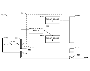
[0017] FIG. 1 depicts an example process control system 100 including a
multiple-contact
switch 102 to control a process control device, which in this example is
depicted as a valve.
- 3 -
CA 02852047 2014-04-11
WO 2013/059091 PCT/US2012/059997
The example process control system 100 of FIG. 1 monitors a level of a liquid
104 in a
vessel, container, or liquid tank 106 using a sensor such as a liquid level
detector 108. The
example multiple-contact switch 102 is mechanically coupled to the liquid
level detector 108
to determine whether a liquid level 110 sensed by a physical position of the
liquid level
detector 108 is higher (or lower) than a threshold level 112. As the liquid
level 110 increases
or decreases, the physical position of the liquid level detector 108 rises and
falls, respectively.
The example multiple-contact switch 102 outputs a signal having two possible
values (e.g.,
open/close, on/off, etc.) to a microcontroller 114. Thus, the value of the
output signal from
the multiple-contact switch 102 is dependent on whether the liquid level 110
(e.g.,
determined by the physical position of the liquid level detector 108) is
higher (or lower) than
the threshold level 112.
[0018] To output a signal, the example multiple-contact switch 102 of FIG.
1 includes a
double-throw switch 116, a first throw circuit 118, and a second throw circuit
120. The
example double-throw switch 116 connects a common contact to one of the first
throw circuit
118 or the second throw circuit 120 at any given time. Based on which of the
example throw
circuits 118, 120 to which the double-throw switch is connected to the common
contact (e.g.,
whether the liquid level 110 is above (or below) the threshold level 112), the
example
multiple-contact switch 102 (e.g., the first throw circuit 118 or the second
throw circuit 120)
outputs one of two possible output values.
[0019] The example microcontroller 114 of FIG. 1 causes an actuator 122 to
open or close
a valve 124 based on the signal output from the example multiple-contact
switch 102. In the
example of FIG. 1, the example microcontroller 114 causes the actuator 122 to
open the valve
124 when the liquid level 110 is higher than the threshold level 112. Opening
the example
valve 124 causes liquid 104 from the liquid tank 106 to exit the liquid tank
106 via an exit
fluid passage 126, thereby lowering the liquid level 110. Conversely, the
example
microcontroller 114 causes the actuator 122 to close the valve 124 when the
liquid level 110
is below the threshold level 112. Closing the example valve 124 stops the
liquid 104 from
exiting the tank 106.
[0020] FIG. 2 depicts another example process control system 200 including
a multiple-
contact switch 202 to control a valve. Like the example multiple-contact
switch 102 of FIG.
1, the example multiple-contact switch 202 includes the double-throw switch
116 coupled to
one of a first throw circuit 204 or a second throw circuit 206 at any given
time. Additionally,
the example multiple-contact switch outputs a first output signal from the
first throw circuit
204 to a microcontroller 208. However, unlike the example multiple-contact
switch 102, the
- 4 -
CA 02852047 2014-04-11
WO 2013/059091 PCT/US2012/059997
example multiple-contact switch 202 of FIG. 2 also outputs a second output
signal from the
second throw circuit 206. The first throw circuit 204 and the second throw
circuit 206 output
the first and second output signals based on whether the example double-throw
switch 116 is
electromechanically coupled to the first throw circuit 204 or the second throw
circuit 206.
[0021] The example microcontroller 208 of FIG. 2 receives the first and
second output
signals from the multiple-contact switch 202 and determines whether the
signals correspond
to a first state (e.g., on, open, etc.), a second state (e.g., off, close,
etc.) or an invalid state
(e.g., an error state). For example, if the first output signal is a logical
high signal and the
second output signal is a logical low signal, the microcontroller 208 may
determine that the
multiple-contact switch 202 is in a first state. Conversely, if the first
output signal is a logical
low signal and the second output signal is a logical high signal, the
microcontroller 208 may
determine that the multiple-contact switch 202 is in a second state. If the
first and second
output signals have the same logical value (e.g., high or low), the example
microcontroller
208 may determine that an invalid state has occurred (e.g., the double throw
switch 116 is not
in contact with either of the throw circuits 204, 206, a circuit problem has
occurred, etc.).
[0022] FIG. 3 is a schematic diagram of an example multiple-contact switch
300 to control
the process control device (e.g., the valve 124). The example multiple-contact
switch 300
may be used to implement the multiple-contact switch 102 of FIG. 1. As shown
in FIG. 3,
the example multiple-contact switch 300 includes a double throw switch 302, a
first throw
circuit 304, and a second throw circuit 306. The first throw circuit 304 is
coupled to a first
terminal 308 of the double throw switch 302, and outputs a first or second
signal to a
microcontroller (e.g., the microcontroller 114 of FIG. 1) based on the
position of the example
double throw switch 302. The example second throw circuit 306 is coupled to a
second
terminal 310 of the example double throw switch 302, and causes the first
throw circuit 304
to output the first or second signal based on the position of the example
double throw switch
302.
[0023] The example double throw switch 302 of FIG. 3 includes the first and
second
terminals 308, 310 and a common terminal 312. The common terminal 312 is
switched
between the terminals 308, 310. The example common terminal 312 is generally
electromechanically coupled to one of the first or second terminals 308, 310
at any given
time, with the exception that the example double throw switch 302 uses a break-
before-make
method when switching between the terminals 308, 310. The example common
terminal 312
is electrically coupled to a reference signal (e.g., ground). The example
reference signal of
- 5 -
CA 02852047 2014-04-11
WO 2013/059091
PCT/US2012/059997
FIG. 3 corresponds to one of the output signals, such as a low, off, or
logical zero signal. A
contrasting high, on, or logical one signal is a voltage reference 314.
[0024] The example first throw circuit 304 includes a two-input not-and (NAND)
logic
gate 316 and a pull-up resistor 318. A first terminal of the NAND gate 316 is
coupled to the
first terminal 308 of the double throw switch 302 and to the high reference
314 via the pull-
up resistor 318. Similarly, the example second throw circuit 306 includes a
two-input not-
and (NAND) logic gate 320 and a pull-up resistor 322. A first terminal of the
NAND gate
320 is coupled to the second terminal 310 of the double throw switch 302 and
to the high
reference 314 via the pull-up resistor 322. The output of the NAND gate 320 is
input to the
second terminal of the NAND gate 316. The output of the NAND gate 316 is input
to the
second terminal of the NAND gate 320 and is used as the output of the example
multiple-
contact switch 300.
[0025] In combination, the example first and second throw circuits 304, 306
ensure that
the output from the multiple-contact switch 300 of FIG. 3 to the
microcontroller 114 does not
change states unless the common contact 312 changes from being coupled to one
of the
terminals 308, 310 to the other one of the terminals 308, 310. For example,
the first and
second throw circuits 304, 306 maintain the state of the output signal if
there is
electromechanical bouncing (e.g., rapid connection and disconnection) between
the common
terminal 312 and one of the terminals 308, 310.
[0026] An example of operation of the multiple-contact switch 300 of FIG. 3
is described
below. In describing the example operation, the common terminal 312 and the
reference to
which it is coupled (e.g., ground) will be referred to as a low signal, and
the high reference
314 (e.g., a supply signal) will be referred to as a high signal. The low and
high signals are
used as logical states. In operation, the common terminal 312 may be coupled
to the second
terminal 310 at a first time. As a result, the first terminal of the NAND gate
320 is pulled to
the low signal, thereby causing the NAND gate 320 to output a high signal to
the second
input terminal of the NAND gate 316. The first terminal of the NAND gate 316
is pulled to
the high signal via the pull-up resistor 318. Because both input terminals to
the NAND gate
316 are a high signal, the output of the NAND gate (and the output of the
multiple-contact
switch 300) to the microcontroller 114 is a low signal.
[0027] At a second time after the first time, the example double throw switch
302 may
switch the common terminal 312 to connect to the first terminal 308. The first
terminal 308
and, thus, the first terminal of the NAND gate 316 is pulled to the low
signal, causing the
output of the NAND gate 316 to become a high signal. The high signal output
from the
- 6 -
CA 02852047 2014-04-11
WO 2013/059091 PCT/US2012/059997
NAND gate 316 is input to the first terminal of the NAND gate 320. The second
terminal of
the NAND gate 320 is pulled to the high signal by the pull-up resistor 322.
Because both
input terminals to the NAND gate 320 are a high signal, the output of the NAND
gate 320 is
a low signal. This low signal is input to the second terminal of the NAND gate
316.
[0028] At a third time after the second time, the example double throw switch
302
experiences bouncing and rapid electromechanical connection and disconnection
with the
first terminal 308. While the first terminal 308 is temporarily disconnected
from the common
terminal 312 (e.g., the low signal), the first terminal of the NAND gate 316
may be pulled up
to the high signal via the pull-up resistor 318. However, the output of the
example NAND
gate 316 does not change to the low signal because the input to the second
terminal of the
NAND gate 316 remains at the low signal. Similarly, if the double throw switch
302
experiences bouncing with the second terminal 310 at the first time discussed
above, the
output from the example NAND gate 320 does not change because the input to the
first
terminal of the NAND gate 320 remains at the low signal despite the bouncing.
Thus, the
example multiple-contact switch 300 of FIG. 3 is desensitized to or immune
from bouncing
without requiring time-delay and/or other circuitry that reduces the
responsiveness of the
multiple-contact switch 300.
[0029] While the example multiple-contact switch 300 includes NAND gates and
pull-up
resistors, and high and low signals, any other types of logic gates, signal
levels, and/or pull-
up and/or pull-down resistors may be used to obtain similar functionality.
[0030] FIG. 4 is a schematic diagram of another example multiple-contact
switch 400 to
control a process control device. The example multiple-contact switch 400 may
be used to
implement the multiple-contact switch 102 of FIG. 1. As shown in FIG. 4, the
example
multiple-contact switch 400 includes the example double throw switch 302 of
FIG. 3, a first
throw circuit 402, and a second throw circuit 404. As described above, the
example double
throw switch 302 includes the first and second terminals 308, 310, and a
common terminal
312 electrically coupled to a reference (e.g., a low signal).
[0031] The example first throw circuit 402 of FIG. 4 includes an inverter or a
NOT logic
gate 406 and a pull-up resistor 408. Similarly, the example second throw
circuit 404 includes
a NOT logic gate 410 and a pull-up resistor 412. The output of the example
first throw
circuit 402 (e.g., the output of the NOT gate 406) is input to a
microcontroller (e.g., the
example microcontroller 114 of FIG. 1). The first terminal 308 of the double
throw switch
302 is coupled to the input terminal of the example NOT gate 406. The output
of the NOT
gate 406 is pulled-up to a supply reference 414 (e.g., a high signal) via the
pull-up resistor
- 7 -
CA 02852047 2014-04-11
WO 2013/059091 PCT/US2012/059997
408. The second terminal 310 of the double throw switch 302 is coupled to the
input terminal
of the example NOT gate 410, which is also coupled to the output of the NOT
gate 406. The
output of the example NOT gate 410 is also pulled up to the supply reference
414 via the
pull-up resistor 412 and is coupled to the input terminal of the NOT gate 406.
[0032] An example of operation of the multiple-contact switch 400 of FIG. 4
is described
below. In describing the example, the common terminal 312 and the reference to
which it is
coupled (e.g., ground) will be referred to as a low signal, and the high
reference 414 (e.g., a
supply signal) will be referred to as a high signal. The low and high signals
correspond to
logical states. In operation, the example common terminal 312 is coupled to
the second
terminal 310 at a first time. As a result, the output of the multiple-contact
switch 400 is
coupled directly to the low signal. Additionally, the input to the example NOT
gate 410 is a
low signal, causing the output of the NOT gate 410 to be a high signal. The
high signal
output from the NOT gate 410 is input to the NOT gate 406, resulting in a low
output from
the NOT gate 406 consistent with being coupled to the common terminal 312.
[0033] At a second time after the first time, the common terminal 312 is
decoupled from
the second terminal 310 and coupled to the first terminal 308. At that time,
the input to the
example NOT gate 406 is a low signal, causing the NOT gate 406 to output a
high signal
from the multiple-contact switch 400 to the example microcontroller 114. The
output from
the NOT gate 406 is also input to the example NOT gate 410, causing the NOT
gate 410 to
output a low signal. The low signal is directly coupled to the first terminal
308 and is
consistent with being connected to the common terminal 312.
[0034] At a third time after the second time, the example double throw switch
302
experiences bouncing and rapid electromechanical connection and disconnection
with the
first terminal 308. While the first terminal 308 is temporarily disconnected
from the common
terminal 312 (e.g., the low signal), the input terminal to the NOT gate 406 is
disconnected
from the common terminal 312. However, the low signal output from the example
NOT gate
410 maintains the low signal input to the NOT gate 406, which causes the NOT
gate 410 to
maintain the high output signal to the example microcontroller 114. Similarly,
if the double
throw switch 302 experiences bouncing with the second terminal 308 at the
first time
discussed above, the output from the example NOT gate 406 does not change
because the
input terminal of the NOT gate 410 remains at the low signal despite the
bouncing due to the
output from the NOT gate 406. Thus, the example multiple-contact switch 400 of
FIG. 4 is
desensitized or even immune from bouncing without requiring time-delay and/or
other
circuitry that reduces the responsiveness of the multiple-contact switch 400.
- 8 -
CA 02852047 2014-04-11
WO 2013/059091 PCT/US2012/059997
[0035] While the example multiple-contact switch 400 includes NOT gates and
pull-up
resistors, and high and low signals, any other types of logic gates, signal
levels, and/or pull-
up and/or pull-down resistors may be used to obtain similar or equivalent
functionality.
[0036] FIG. 5 is a schematic diagram of another example multiple-contact
switch 500 to
control a process control device. The example multiple-contact switch 500 may
be used to
implement the multiple-contact switch 202 of FIG. 2. As shown in FIG. 5, the
example
multiple-contact switch 500 includes the example double throw switch 302 of
FIG. 3, as well
as a first throw circuit 502 and a second throw circuit 504. The first throw
circuit 502 is
coupled to the first terminal 308 of the double throw switch 302, and outputs
a first signal to
a microcontroller (e.g., the microcontroller 114 of FIG. 1) based on the
position of the
example double throw switch 302. The example second throw circuit 504 is
coupled to the
second terminal 310 of the example double throw switch 302 and outputs a
second signal to
the microcontroller 114 based on the position of the double throw switch 302.
[0037] The example first throw circuit 502 includes a pull-up resistor 506
to pull-up the
first terminal 308 and the output of the first throw circuit 502 to a high
reference 508.
Similarly, the second throw circuit 504 includes a pull-up resistor 510 to
pull-up the second
terminal 310 and the output of the second throw circuit 504 to the high
reference 508. In
operation, the example double throw switch 302 connects the common terminal
312 to one of
the first or second terminals 308, 310. When the first terminal 308 is coupled
to the common
terminal 312, the first throw circuit 502 outputs a low signal to the
microcontroller 114 and
the second throw circuit 504 outputs a high signal to the microcontroller 114.
Conversely,
when the second terminal 310 is coupled to the common terminal 312, the first
throw circuit
502 outputs a high signal to the microcontroller 114 and the second throw
circuit 504 outputs
a low signal to the microcontroller 114.
[0038] The example microcontroller 114 determines a state of the multiple-
contact switch
500 based on the combination of outputs from the first and second throw
circuits 502, 504.
For example, if the output from the first throw circuit 502 is a high signal
and the output from
the second throw circuit 504 is a low signal, the microcontroller 114
determines that the
multiple-contact switch 114 is in a first state. Conversely, if the output
from the first throw
circuit 502 is a low signal and the output from the second throw circuit 504
is a high signal,
the microcontroller 114 determines that the multiple-contact switch 114 is in
a second state.
In the example of FIG. 5, the microcontroller 114 detects an error if both
outputs from the
multiple-contact switch 500 are low signals, because such a condition may
correspond to a
malfunction of the switch 500. If the microcontroller 114 detects that both
outputs from the
- 9 -
CA 02852047 2014-04-11
WO 2013/059091 PCT/US2012/059997
multiple-contact switch 500 are high signals, the microcontroller determines
that the example
multiple-contact switch 500 may be experiencing bouncing and/or some other
error. In
response to detecting that both outputs are high signals, the microcontroller
114 samples the
outputs from the multiple-contact switch 500 multiple times to determine
whether either of
the outputs has changed to a low signal and/or to determine whether one of the
outputs has
stopped bouncing. For example, if the microcontroller 114 detects that a
threshold number of
consecutive samples of the output signal from the example second throw circuit
504 are low
signals while the output signal from the first throw circuit remains high, the
multiple-contact
switch 500 has changed to the first state. In some examples, the
microcontroller 114 may
determine that an error condition exists if a certain amount of time elapses
(or other condition
occurs) without the multiple-contact switch 500 achieving the first state or
the second state.
[0039] While the example multiple-contact switch 500 includes pull-up
resistors and high
and low signals, any other types of signal levels, logic, and/or pull-up
and/or pull-down
resistors may be used to obtain similar or equivalent functionality.
Additionally, while the
example multiple contact switches 300, 400 of FIGS. 3 and 4 are illustrated as
having a single
output signal to the microcontroller 114, either of the example switches 300,
400 may output
second signals (e.g., from the respective second throw circuits 306, 404) to
the
microcontroller 114. In some such examples, the microcontroller 114 may
implement state-
detecting and/or error-detecting methods such as the example state-detecting
and/or error-
detecting methods described above with reference to FIG. 5.
[0040] FIG. 6 is a schematic diagram of another example multiple-contact
switch 600 to
control a process control device. The example multiple-contact switch 600 of
FIG. 6 includes
a double throw switch 602, first and second throw circuits 604, 606, and an
error trigger 608.
The example double throw switch 602 of FIG. 6 may be implemented using the
example
double throw switch 302 of FIGS. 3-5. The example first and second throw
circuits 604, 606
may be implemented using the example first and second throw circuits 304, 306
of FIG. 3,
the example first and second throw circuits 402, 404 of FIG. 4, the example
first and second
throw circuits 502, 504 of FIG. 5, and/or any other equivalent, similar,
and/or different
configurations of throw circuits. Accordingly, the example first and second
throw circuits
604, 606 may or may not be interconnected as illustrated in FIG. 6 by a dashed
line
connecting the throw circuits 604, 606.
[0041] The example error trigger 608 triggers error detection by the
microprocessor 114
via the first and second throw circuits 604, 606 when an external error
condition occurs. To
trigger error detection, the error trigger 608 may cause the outputs of both
throw circuits 604,
- 10-
CA 02852047 2014-04-11
WO 2013/059091 PCT/US2012/059997
606 to be low signals or high signals. An external error condition includes
errors not caused
by internal malfunction of the example multiple-contact switch 600 and/or the
microcontroller 114. An example external error condition may include a loss of
an external
source of power to the multiple-contact switch 600 and/or the microcontroller
114. In such
an example, the error trigger 608, such as a controller of an uninterruptible
power supply
(UPS), controls the first and second throw circuits 604, 606 to output low
signals to the
microcontroller (e.g., in response to detecting loss of supply power and use
of power stored in
the UPS). In the example, the UPS provides power to the multiple-contact
switch 600, to the
microcontroller 114, and/or to a process control device controlled by the
microcontroller 114
to change the state of the process control device to a predetermined or
default safety
condition. An example safety condition may include controlling the actuator
122 to close the
example valve 124 of FIG. 1. The example microcontroller 114 may use the
example state-
detecting and/or error-detecting methods described above with reference to
FIG. 5 to detect
the state(s) and/or error(s) in the example multiple-contact switch 600,
including error(s)
triggered by the example error trigger 608 via the first and second throw
circuits 604, 606.
[0042] FIG. 7 is a flowchart representative of an example process 700 that
may be used to
implement the example microcontroller 114 of FIGS. 1-6 to control a process
control device
based on input from a multiple-contact switch.
[0043] The example process 700 of FIG. 7 begin by detecting (e.g., via the
microcontroller
114 of FIGS. 1-6) output signal(s) from a multiple-contact switch (e.g., the
multiple-contact
switches 102, 202, 300, 400, 500, and/or 600 of FIGS. 1-6) (block 702). For
example, the
microcontroller 114 may receive one or more output signal(s) from respective
throw circuits
118, 120, 204, 206, 304, 306, 402, 404, 502, 504, 604, 606 of FIGS. 1-6). The
example
microcontroller 114 determines if the output signal(s) correspond to a first
state (block 704).
If the output signal(s) correspond to the first state (block 704), the example
microcontroller
114 actuates a process control device based on the first state (block 706).
For example, the
microcontroller 706 may cause a valve actuator to open a valve in response to
the first state.
After actuating the process control device (block 706), control returns to
block 702 to detect
the output signal(s).
[0044] If the output signal(s) do not correspond to the first state (block
704), the example
microcontroller 114 determines if the output signal(s) correspond to a second
state (block
708). If the output signal(s) correspond to the second state (block 708), the
example
microcontroller 114 actuates a process control device based on the second
state (block 710).
For example, the microcontroller 114 may cause a valve actuator to close a
valve in response
- 11-
CA 02852047 2014-04-11
WO 2013/059091
PCT/US2012/059997
to the second state. After actuating the process control device (block 710),
control returns to
block 702 to detect the output signal(s).
[0045] If the output signal(s) do not correspond to the second state (block
708), the
example microcontroller 114 determines if the output signal(s) correspond to
an error (block
712). For example, the output signal(s) may correspond to an error if the
output signal(s) are
consistent with a malfunction of the multiple-contact switch. If the output
signal(s)
correspond to an error (block 712), the example microcontroller 114 actuates
the process
control device to a default (e.g., predetermined) error state (block 714).
After actuating the
process control device to the default error state (block 714), the example
process 700 of FIG.
7 ends.
[0046] If the output signal(s) do not correspond to an error (block 712),
the example
microcontroller 114 determines whether bouncing is detected (block 716). For
example,
bouncing may be detected when different ones of the output signal(s)
correspond to different
ones of the first and second states. If bouncing is not detected (block 716),
control returns to
block 702 to detect the output signal(s). On the other hand, if bouncing is
detected (block
716), the example microcontroller 114 samples the output signal(s) (block
718). For
example, the microcontroller 114 may sample the output signal(s) multiple
times to obtain
consecutive samples.
[0047] The example microcontroller 114 then determines whether a threshold
number X
of consecutive output signal(s) have the same value (block 720). If the
threshold number X
of consecutive output signal(s) have the same value (block 720), the example
microcontroller
114 determines that the bouncing has ended and returns to block 704 to
determine the state of
the output signal(s). If a threshold number of output signal(s) having the
same value has not
been found (block 720), the example microcontroller 114 determines whether a
time limit has
been reached (block 722). If the time limit has not been reached (block 722),
control returns
to block 718 to continue sampling output signal(s). On the other hand, if the
time limit has
been reached (block 722), the example microcontroller 114 actuates the process
control
device to the default error state (block 714). The example process 700 of FIG.
7 may then
end.
[0048] Although certain example apparatus and methods have been described
herein, the
scope of coverage of this patent is not limited thereto. On the contrary, this
patent covers all
apparatus and methods fairly falling within the scope of the claims of this
patent.
- 12-