Note: Descriptions are shown in the official language in which they were submitted.
CA 02852405 2014-05-21
Atty. Dkt. No. 20121660CA01
,
PRINTING APPARATUS USING ELECTROHYDRODYNAMICS
BACKGROUND
[0001] The present disclosure relates to systems and methods for
printing using
an electrohydrodynamic liquid delivery method. These systems and methods can
be
used in conjunction with electrophotographic imaging members.
[0002] Electrophotographic or xerographic reproductions may be
initiated by
depositing a uniform charge on an imaging member, i.e. photoreceptor, followed
by
exposing the imaging member to a light image of an original document. Exposing
the
charged imaging member to a light image causes discharge in areas
corresponding
to non-image areas of the original document while the charge is maintained on
image areas, creating an electrostatic latent image of the original document
on the
imaging member. The latent image is subsequently developed into a visible
image
by depositing a charged ink (i.e. toner), onto the photoconductive surface
layer, such
that the developing material is attracted to the charged image areas on the
imaging
member. Thereafter, the developing material is transferred from the imaging
member to a copy sheet or some other image support substrate to which the
image
may be permanently affixed for producing a reproduction of the original
document. In
a final step in the process, the imaging member is cleaned to remove any
residual
developing material therefrom, in preparation for subsequent imaging cycles.
However, xerographic printing has been partially constrained by its operation
flexibility, printing resolution, and materials generally.
[0003] On the other hand, inkjet printing has been well known for
use in printing
images as well as used in the fabrication of printed circuits by directly
printing
components on an arbitrary blanket with few materials limitations. Recently,
functional inks have been designed from organic materials and deposited for
more
versatile uses in energy harvesting, sensing, information display, drug
discovery,
MEMS devices, and other areas. Two common methods for ink-jet printing are
based on thermal or acoustic formation and ejection of liquid droplets through
a
nozzle aperture. Conventional inkjets have a resolution limited to from about
20 to
about 30 pm.
CA 02852405 2014-05-21
Atty. Dkt. No. 20121660CA01
[0004] It would be desirable to develop systems and methods for applying
ink to
an imaging member surface which permit accurate control of the amount of the
ink
without degrading image quality.
BRIEF DESCRIPTION
[0005] The present disclosure relates to systems and methods for
electrohydrodynamically jetting ink onto an imaging member surface. The
systems
and methods permit accurate control of the amount of the ink without degrading
image quality.
[0006] Disclosed in embodiments is an image forming apparatus which
includes
an electrophotographic imaging member having a charge-retentive surface; a
charging unit for applying an electrostatic charge on the charge-retentive
surface to
a predetermined electric potential; a light unit to discharge the
electrostatic charge
on the charge retentive surface to form a discharge area; a development
component
to apply an ink to the charge-retentive surface to form a developed image; a
transfer
component for transferring the developed image from the charge-retentive
surface to
another member or a copy substrate; an optional cleaning system to clean the
imaging member surface; and a voltage bias unit for adjusting an electric
field
between the development component and the imaging member surface. The
imaging member surface is spaced apart from the development component. The
development component comprises a reservoir for containing the ink and one or
more capillary openings through which the ink can be provided to the imaging
member electrohydrodynamically when the electric field is generated.
[0007]
[0008] The one or more capillary openings may be located from about 10 pm
to
about 200 pm from the imaging member surface. In some embodiments, the one or
more capillary openings are located from about 50 pm to about 100 pm from the
imaging member surface.
[0009] The discharged area may have a lateral resolution less than 50 pm.
[0010] The capillary openings may have an area in the range of from about
0.01
pm2 to about 0.25 mm2.
- 2 -
CA 02852405 2016-04-25
[0011] In some
embodiments, the printing resolution is better than about 50 pm.
The printing resolution may be between about 500 nm and about 500 pm.
[0012] The
charging unit may be in contact, semi-contact, or non-contact with the
imaging member surface.
[0013] In some
embodiments, the electric field strength is in the range of from
about 5 kV/mm to about 10 kV/mm.
[0014] The predetermined electric potential may be in the range of from about
500 V to about 1 kV/mm.
[0015] in some embodiments, the voltage bias unit is configured to
simultaneously provide DC and AC voltages_
[0016] The imaging member surface may have a lower surface energy than a
transfer component surface of the transfer component.
[0017]
Disclosed in other embodiments is a method for providing an ink to an
imaging member surface. The method includes forming an electrostatic latent
image
on an imaging member surface; and generating an electric field between the
imaging
member surface and a development component. The development component is
not in physical contact with the imaging member surface. The development
component includes a reservoir containing the ink and one or more capillary
openings.
[0018] The
electrostatic latent image may be formed by uniformly charging the
imaging member surface with a charging member and selectively dissipating at
least
a portion of the uniformly charged surface with an image input apparatus to
form the
electrostatic latent image.
[0018a] In
accordance with an aspect, there is provided an image forming
apparatus comprising:
an imaging member having a charge-retentive surface;
a charging unit for applying an electrostatic charge on the charge
retentive surface to a predetermined electric potential;
a light unit to discharge the electrostatic charge on the charge retentive
surface to form a discharged area;
- 3 -
CA 02852405 2016-04-25
a development component to apply an ink to the charge-retentive
surface to form a developed image; and
a transfer component for transferring the developed image from the
charge-retentive surface to another member or a copy substrate; and
a voltage bias unit for adjusting an electric field between the
development component and the imaging member surface;
wherein the imaging member surface is spaced apart from the
development component; and
wherein the development component comprises a reservoir containing
the ink and a plurality of capillary openings directed towards the imaging
member
surface;
wherein an electrode is present at the capillary openings to provide
electrical charge and form the electric field between the development
component
and the imaging member.
[0018b] In
accordance with an aspect, there is provided a method for providing
an ink to an imaging member surface, comprising:
forming an electrostatic latent image on an imaging member surface;
and
generating an electric field between the imaging member surface and a
development component;
wherein the development component is not in physical contact with the
imaging member surface; and
wherein the development component comprises a reservoir containing
the ink and a plurality of capillary openings, the ink being
electrohydrodynamically
delivered to the imaging member surface when the electric field is generated,
and an
electrode is present at the capillary openings to provide electrical charge
and form
the electric field between the development component and the imaging member
surface.
[0019] These
and other non-limiting characteristics of the disclosure are more
particularly disclosed below.
- 3a -
CA 02852405 2016-04-25
_
BRIEF DESCRIPTION OF THE DRAWINGS
[0020] The
following is a brief description of the drawings, which are presented
for the purposes of illustrating the exemplary embodiments disclosed herein
and not
for the purposes of limiting the same.
- 3b -
CA 02852405 2014-05-21
Atty. Dkt. No. 201216600A01
[0021]
FIG. 1 illustrates an exemplary image forming apparatus of the present
disclosure.
[0022]
FIG. 2 illustrates an exemplary development component of the present
disclosure.
[0023]
FIG. 3 is a cross-sectional view of an exemplary embodiment of a
photoreceptor drum having a single charge transport layer.
[0024]
FIG. 4 is a cross-sectional view of another exemplary embodiment of a
photoreceptor drum having a single charge transport layer.
[0025]
FIG. 5 is a picture of an experimental setup illustrating the processes and
devices of the present disclosure.
DETAILED DESCRIPTION
[0026] A more complete understanding of the components, processes and
apparatuses disclosed herein can be obtained by reference to the accompanying
drawings.
These figures are merely schematic representations based on
convenience and the ease of demonstrating the present disclosure, and are,
therefore, not intended to indicate relative size and dimensions of the
devices or
components thereof and/or to define or limit the scope of the exemplary
embodiments.
[0027]
Although specific terms are used in the following description for the sake
of clarity, these terms are intended to refer only to the particular structure
of the
embodiments selected for illustration in the drawings, and are not intended to
define
or limit the scope of the disclosure. In the drawings and the following
description
below, it is to be understood that like numeric designations refer to
components of
like function.
[0028] The
singular forms "a," "an," and "the" include plural referents unless the
context clearly dictates otherwise.
[0029]
Numerical values in the specification and claims of this application should
be understood to include numerical values which are the same when reduced to
the
same number of significant figures and numerical values which differ from the
stated
- 4 -
CA 02852405 2014-05-21
Atty. Dkt. No. 201216600A01
value by less than the experimental error of conventional measurement
technique of
the type described in the present application to determine the value.
[0030] All ranges disclosed herein are inclusive of the recited endpoint
and
independently combinable (for example, the range of "from 2 grams to 10 grams"
is
inclusive of the endpoints, 2 grams and 10 grams, and all the intermediate
values).
The endpoints of the ranges and any values disclosed herein are not limited to
the
precise range or value; they are sufficiently imprecise to include values
approximating these ranges and/or values.
[0031] A value modified by a term or terms, such as "about" and
"substantially,"
may not be limited to the precise value specified. The approximating language
may
correspond to the precision of an instrument for measuring the value. The
modifier
"about" should also be considered as disclosing the range defined by the
absolute
values of the two endpoints. For example, the expression "from about 2 to
about 4"
also discloses the range "from 2 to 4."
[0032] "Electrohydrodynamic" refers to ejecting a fluid under an electric
charge
applied to the orifice region of the nozzle. When the electrostatic force is
sufficiently
large to overcome the surface tension of the fluid at the nozzle, fluid is
ejected from
the nozzle.
[0033] "Ejection orifice" refers to the region of the nozzle from which the
fluid is
capable of being ejected under an electric charge. The "ejection area" of the
ejection
orifice refers to the effective area of the nozzle facing the substrate
surface. In an
embodiment, the ejection area corresponds to a circle, so that the diameter of
the
ejection orifice (D) is calculated from the ejection area (A) by: D =
sqrt(4A/pi). A
"substantially circular" orifice refers to an orifice having a generally
smooth-shaped
circumference (e.g., no distinct, sharp corners), where the minimum length
across
the orifice is at least 80% of the corresponding maximum length across the
orifice
(such as an ellipse whose major and minor diameters are within 20% of each
other).
"Average diameter" is calculated as the average of the minimum and maximum
dimension. Similarly, other shapes are characterized as substantially shaped,
such
as a square, rectangle, triangle, where the corners may be curved and the
lines may
- 5 -
CA 02852405 2014-05-21
Atty. Dkt. No. 20121660CA01
be substantially straight. In an aspect, substantially straight refers to a
line having a
maximum deflection position that is less than 10% of the line length.
[0034] "Electric charge" refers to the potential difference between the
printing
fluid within the nozzle (e.g., the fluid in the vicinity of the ejection
orifice) and the
substrate surface. This electric charge may be generated by providing a bias
or
electric potential to one electrode compared to a counter electrode.
[0035] A variety of efforts have been attempted for developing
electrohydrodynamic printing (i.e., to use electric field to create fluid
flows to deliver
ink to a substrate). Although some of them have demonstrated
electrohydrodynamic
printing resolution down to submicron meter, flexibility to integrate nozzle
array and
high¨speed application have not been well established. Without patterned
charges
on substrate, there is much higher possibility for cross¨talking of ink
droplets (i.e.
droplets landing other than in their intended location). As a result, jetting
frequency,
lateral separation of the nozzle array and tip¨substrate distance play coupled
roles.
Simultaneous jetting of multiple ink drops for this setup cannot be maximized.
[0036] The present disclosure relates to image forming apparatuses that
include
a development component for electrohydrodynamically applying an ink to a
charge-
retentive surface of an imaging member. The development component is not in
physical contact with the imaging member surface (i.e., there is a gap between
the
development component and the imaging member surface).
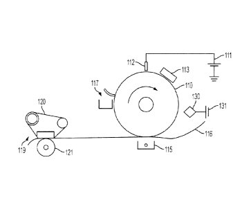
[0037] Referring to FIG. 1, the structure of an imaging member using the
delivery
member is depicted. In the depicted embodiment, the imaging member surface 110
rotates clockwise. The charge-retentive surface of imaging member 110 is
charged
by a charging unit/member (e.g., a bias charging roller) 112 to which a
voltage has
been supplied from power supply 111. The charging unit 112 may be in contact,
semi-contact, or non-contact with the imaging member surface 110. The charging
unit is configured to apply an electrostatic charge on the charge-retentive
surface to
a predetermined electric potential (e.g., from about 500 V to about 1 kV). The
imaging member is then imagewise exposed to light from an optical system or an
image input apparatus 113, such as a light unit (e.g., a laser or a light
emitting
- 6 -
CA 02852405 2014-05-21
Atty. Dkt. No. 20121660CA01
diode), to form an electrostatic latent image thereon.
Exposure to the light
selectively dissipates the charge on the imaging member surface.
[0038] The
electrostatic latent image is developed by bringing a developer
mixture from development component 130 into contact therewith. Development
component 130 is charged by power supply/voltage bias unit 131, which in some
embodiments is the same as power supply 111 which powers charging member 112.
The development component 130 contains an ink which can be
electrohydrodynamically applied to the imaging member surface 110 when an
electric field is generated between the development component 130 and the
imaging
member surface 110. The development component is selectively applied to form a
developed image on the imaging member surface 110. The developed image may
be formed on those areas of the imaging member surface 110 which have retained
a
charge.
[0039]
Application of an electric charge establishes an electric field that results
in
controllable printing of the ink on the imaging member surface. The electric
charge
can be applied intermittently at a given frequency. The pulsed voltage or
electric
charge may be a square wave, sawtooth, sinusoidal, or combinations thereof.
[0040]
After the ink has been deposited on the photoconductive surface, the
developed image is transferred to a copy substrate 116 by transfer component
115,
which can utilize pressure transfer or electrostatic transfer. Alternatively,
the
developed image can be transferred to an intermediate transfer member, or bias
transfer member, and subsequently transferred to a copy substrate. Examples of
copy substrates include paper, transparency material such as polyester,
polycarbonate, or the like, cloth, wood, or any other desired material upon
which the
finished image will be situated. After the transfer of the developed image is
completed, copy substrate 116 advances to fusing member 119, depicted as fuser
belt 120 and pressure roll 121, wherein the developed image is fused to copy
substrate 116 by passing the copy substrate between the fuser belt and
pressure
roll, thereby forming a permanent image. Alternatively, transfer and fusing
can be
effected by a transfix application. The imaging member 110 then advances to
- 7 -
CA 02852405 2014-05-21
Atty. Dkt. No. 20121660CA01
cleaning station 117, wherein any remaining toner is cleaned therefrom by use
of a
blade, brush, or other cleaning apparatus.
[0041] A surface of the transfer component 115 may have greater surface energy
than the imaging member surface.
[0042] The voltage provided by the power supply or power supplies may be
provide standard line voltage(s) or other voltage levels or signal frequencies
which
may be desirable in accordance with other limiting factors dependent upon
individual
machine design. The power supply or power supplies may provide a DC voltage,
an
AC voltages, or combinations thereof. In some embodiments, the power supply or
power supplies are configured to provide AC and DC voltages simultaneously.
[0043] The power supply or power supplies may be a high voltage power
supply
or power supplies. The electric field strength may be in the range of from
about 5
kV/mm to about 10 kV/mm. In some embodiments, the electric field may be
greater
than or equal to 100 kV/m. The electric field may be calculated by dividing
the
applied voltage by the distance between the development component 130 and the
imaging member surface 110. The distance may be from about 10 pm to about 200
pm. For example, at a distance of about 3 cm, an applied voltage of about 9 kV
would generate an electric field of about 300 kV/m.
[0044] FIG. 2 is a cross-sectional view showing the various parts of a
development component 230 suitable for electrohydrodynamic (EHD) application
of
ink. The development component includes a reservoir 232 and one or more
capillaries 234 extending therefrom to one or more capillary openings 236. The
reservoir 232 contains the ink. When an electric field is applied between the
development component 230 and a surface of the imaging member, the ink is
pulled
from the reservoir 232 via the one or more capillaries 234 and ejected onto
the
imaging member surface via the plurality of capillary openings 236. An
electrode
238 can be present at the capillary opening to provide electrical charge and
form the
electrical field between the development component and the imaging member.
Alternatively, the capillary itself can be made from a conductive material, or
coated
with a conductive material, that serves as an electrode. The reservoir and the
capillaries can be one integral component, or can be fluidly connected to each
other.
- 8 -
CA 02852405 2014-05-21
Atty. Dkt. No. 20121660CA01
[0045] The capillary openings may have an area in the range of from about
0.01
1Jm2 to about 0.25 mm2. In this regard, it is desirable that the ink be
released from
the delivery member in the form of fine liquid droplets, rather than as a
stream.
[0046] The devices and methods disclosed herein recognize that by
maintaining
a smaller nozzle size, the electric field can be better confined to printing
placement
and access smaller droplet sizes. Accordingly, in some aspects of the
disclosure, the
ejection orifices from which printing fluid is ejected are of a smaller
dimension than
the dimensions in conventional inkjet printing. In an aspect the orifice may
be
substantially circular, and have a diameter that is less than 30 micrometers
(pm),
less than 20 pm, less than 10 pm, less than 5 pm, or less than less than 1 pm.
Any
of these ranges are optionally constrained by a lower limit that is
functionally
achievable, such as a minimum dimension that does not result in excessive
clogging, for example, a lower limit that is greater than 100 nm, 300 nm, or
500 nm.
Other orifice cross-section shapes may be used as disclosed herein, with
characteristic dimensions equivalent to the diameter ranges described. Not
only do
these small nozzle diameters provide the capability of accessing ejected and
printed
smaller droplet diameters, but they also provide for electric field
confinement that
provides improved placement accuracy compared to conventional inkjet printing.
The combination of a small orifice dimension and related highly-confined
electric
field provides high-resolution printing.
[0047] Because an important feature in this system is the small dimension
of the
ejection orifice, the orifice is optionally further described in terms of an
ejection area
corresponding to the cross-sectional area of the nozzle outlet. In an
embodiment,
the ejection area is selected from a range that is less than 700 pm2, or
between 0.07
pm2 - 0.12 pm2 and 700 pm2. Accordingly, if the ejection orifice is circular,
this
corresponds to a diameter range that is between about 0.4 pm and 30 pm. If the
orifice is substantially square, each side of the square is between about 0.35
pm and
26.5 pm. In an aspect, the system provides the capability of printing
features, such
as single ion and/or quantum dot (e.g., having a size as small as about 5 nm).
[0048] In an embodiment, any of the systems are further described in terms
of a
printing resolution. The printing resolution is high-resolution, e.g., a
resolution that is
- 9 -
CA 02852405 2014-05-21
Atty. Dkt. No. 201216600A01
not possible with conventional inkjet printing known in the art without
substantial
preprocessing steps. In an embodiment, the resolution is better than 50 pm or
20
pm, better than 10 pm, better than 5 pm, better than 1 pm, between about 5 nm
and
pm, between 100 nm and 10 pm, between 300 nm and 5 pm, or between about
500 nm and about 10 pm. In an embodiment, the orifice area and/or stand-off
distance are selected to provide nanometer resolution, including resolution as
fine as
5 nm for printing single ion or quantum dots having a printed size of about 5
nm,
such as an orifice size that is smaller than 0.15 pm2.
[0049] The discharged area may have a lateral resolution less than 50 pm.
[0050] The nozzle is made of any material that is compatible with the
systems
and methods provided herein. For example, the nozzle is preferably a
substantially
nonconducting material so that the electric field is confined in the orifice
region. In
addition, the material should be capable of being formed into a nozzle
geometry
having a small dimension ejection orifice. In an embodiment, the nozzle is
tapered
toward the ejection orifice. One example of a compatible nozzle material is
microcapillary glass. Another example is a nozzle-shaped passage within a
solid
substrate, whose surface is coated with a membrane, such as silicon nitride or
silicon dioxide.
[0051] Irrespective of the nozzle material, a means for establishing an
electric
charge to the printing fluid within the nozzle, such as fluid at the nozzle
orifice or a
drop extending therefrom, is required. In an embodiment, a voltage source is
in
electrical contact with a conducting material that at least partially coats
the nozzle.
The conducting material may be a conducting metal, e.g., gold, that has been
sputter-coated around the ejection orifice. Alternatively, the conductor may
be a non-
conducting material doped with a conductor, such as an electroconductive
polymer
(e.g., metal-doped polymer), or a conductive plastic. In another aspect,
electric
charge to the printing fluid is provided by an electrode having an end that is
in
electrical communication with the printing fluid in the nozzle.
[0052] Any ink capable of being ionized can generally be used. For example,
the
ink may be made of metal-containing nanoparticles dissolved in a solvent.
Alternatively, the ink can contain conventional emulsion/aggregation toner
particles.
- 10-
CA 02852405 2014-05-21
Atty. Dkt. No. 201216600A01
[0053] The imaging member itself may comprise a substrate 32, optional hole
blocking layer 34, optional adhesive layer 36, charge generating layer 38,
charge
transport layer 40, and an optional overcoat layer 42. Two exemplary
embodiments
of an imaging member are seen in FIG. 3 and FIG. 4.
[0054] The first exemplary embodiment of an imaging member that may be used
in conjunction with the present disclosure is the photoreceptor drum of FIG.
3. The
substrate 32 supports the other layers, and is the central portion of the
drum. An
optional hole blocking layer 34 can also be applied to the substrate, as well
as an
optional adhesive layer 36. Next, the charge generating layer 38 is applied so
as to
be located between the substrate 32 and the charge transport layer 40. If
desired,
an overcoat layer 42 may be placed upon the charge transport layer 40. Thus,
either the charge transport layer or the overcoat layer will be the outermost
exposed
layer of the imaging member, and will provide the surface upon which the
developer
and functional material are applied.
[0055] Another exemplary embodiment of the photoreceptor drum of the present
disclosure is illustrated in FIG. 4. This embodiment is similar to that of
FIG. 3,
except the locations of the charge generating layer 38 and charge transport
layer 40
are reversed. Generally, the charge generating layer, charge transport layer,
and
other layers may be applied in any suitable order to produce either positive
or
negative charging photoreceptor drums.
[0056] The substrate support 32 provides support for all layers of the
imaging
member. It has the shape of a rigid drum and has a diameter necessary for the
imaging application it will be used for. It is generally made from a
conductive
material, such as aluminum, copper, brass, nickel, zinc, chromium, stainless
steel,
aluminum, semitransparent aluminum, steel, cadmium, silver, gold, zirconium,
niobium, tantalum, vanadium, hafnium, titanium, nickel, chromium, tungsten,
molybdenum, indium, tin, and metal oxides.
[0057] An optional hole blocking layer 34 may be applied to the substrate
32 or
coatings. Any suitable and conventional blocking layer capable of forming an
electronic barrier to holes between the adjacent photoconductive layer 38 and
the
underlying conductive surface of substrate 32 may be used.
-11 -
CA 02852405 2016-04-25
[0058] An
optional adhesive layer 36 may be applied to the hole-blocking layer
34. Any suitable adhesive layer well known in the art may be used. Typical
adhesive
layer materials include, for example, polyesters, polyurethanes, and the like,
Satisfactory results may be achieved with adhesive layer thickness between
about
0.05 micrometer (500 angstroms) and about 0.3 micrometer (3,000 angstroms).
Conventional techniques for applying an adhesive layer coating mixture to the
hole
blocking layer include spraying, dip coating, roll coating, wire wound rod
coating,
gravure coating, Bird applicator coating, and the like. Drying of the
deposited coating
may be effected by any suitable conventional technique such as oven drying,
infra
red radiation drying, air drying and the like.
[0069] Any suitable charge generating layer 33 may be applied which can
thereafter be coated over with a contiguous charge transport layer. The charge
generating layer generally comprises a charge generating material and a film-
forming polymer binder resin. Charge generating materials such as vanadyl
phthalocyanine, metal free phthalocyanine, benzimidazole perylene, amorphous
selenium, trigonal selenium, selenium alloys such as selenium-tellurium,
selenium-
tellurium-arsenic, selenium arsenide, and the like and mixtures thereof may be
appropriate because of their sensitivity to white light. Vanadyl
phthalocyanine, metal
free phthalocyanine and tellurium alloys are also useful because these
materials
provide the additional benefit of being sensitive to infrared light. Other
charge
generating materials include quinacridones, dibromo anthanthrone pigments,
benzimidazole perylene, substituted 2,4-diamino-triazines, polynuclear
aromatic
quinones, and the like. Benzimidazole perylene compositions are well known and
described, for example, in U.S. Patent No. 4,587,189. Other suitable charge
generating materials known in the art may also be utilized, if desired. The
charge
generating materials selected should be sensitive to activating radiation
having a
wavelength from about 600 to about 800 nm during the imagewise radiation
exposure step in an electrophotographic imaging process to form an
electrostatic
latent image. In
specific embodiments, the charge generating material is
hydroxygallium phthalocyanine (OHGaPC), chlorogallium phthalocyanine (CIGaPC).
or oxytitanium phthalocyanine (TiOPC).
-12-
CA 02852405 2016-04-25
[0060] Any suitable inactive film forming polymeric material may be employed
as
the binder in the charge generating layer 38, including those described, for
example.
in U.S. Patent No. 3,121,006. Typical organic polymer binders include
thermoplastic
and thermosetting resins such as polycarbonates, polyesters, polyamides,
polyurethanes, polystyrenes, polyarylethers, polyarylsulfones, polybutadienes,
polysulfones, polyethersulfones, polyethylenes, polypropylenes, polyimides,
polymethylpentenes, polyphenylene sulfides, polyvinyl butyral, polyvinyl
acetate,
polysiloxanes, polyacrylates, polyvinyl acetals, polyamides, polyimides, amino
resins, phenylene oxide resins, terephthalic acid resins, epoxy resins,
phenolic
resins, polystyrene and acrylonitrile copolymers, polyvinylchloride,
vinylchloride and
vinyl acetate copolymers, acrylate copolymers, alkyd resins, cellulosic film
formers,
poly(amideimide), styrene-butadiene copolymers, vinylidenechloride-
vinylchloride
copolymers, vinylacetate-vinylidenechioride copolymers, styrene-alkyd resins,
and
the like.
[0061] The charge generating material can be present in the polymer binder
composition in various amounts. Generally, from about 5 to about 90 percent by
weight of the charge generating material is dispersed in about 10 to about 95
percent by weight of the polymer binder, and more specifically from about 20
to
about 70 percent by weight of the charge generating material is dispersed in
about
30 to about 80 percent by weight of the polymer binder.
[0062] The charge generating layer generally ranges in thickness of from
about
0_1 micrometer to about 5 micrometers, and more specifically has a thickness
of
from about 0.3 micrometer to about 3 micrometers. The charge generating layer
thickness is related to binder content. Higher polymer binder content
compositions
generally require thicker layers for charge generation. Thickness outside
these
ranges can be selected in order to provide sufficient charge generation.
[0063] In embodiments, the charge transport layer 40 may comprise from
about
25 weight percent to about 60 weight percent of a charge transport molecule
and
-13-
CA 02852405 2014-05-21
Atty. Dkt. No. 20121660CA01
from about 40 weight percent to about 75 weight percent by weight of an
electrically
inert polymer, both by total weight of the charge transport layer. In specific
embodiments, the charge transport layer comprises from about 40 weight percent
to
about 50 weight percent of the charge transport molecule and from about 50
weight
percent to about 60 weight percent of the electrically inert polymer.
[0064]
Alternatively, the charge transport layer can be formed from a charge
transport polymer. Any suitable polymeric charge transport polymer can be
used,
such as poly(N-vinylcarbazole);
poly(vinylpyrene); poly(vinyltetraphene);
poly(vinyltetracene), and/or poly(vinylperylene).
[0065]
Optionally, the charge transport layer can include materials to improve
lateral charge migration (LCM) resistance such as hindered phenolic
antioxidants
like, for example, tetrakis methylene(3,5-di-tert-butyl-4-hydroxy
hydrocinnamate)
methane (IRGANOX 1010, available from Ciba Specialty Chemical, Tarrytown,
NY), butylated hydroxytoluene (BHT), and other hindered phenolic antioxidants
including SUMILIZERTm BHT-R, MOP-S, BBM-S, WX-R, NW, BP-76 , BP-101, GA-
80, GM, and GS (available from Sumitomo Chemical America, Inc., New York, NY),
IRGANOX 1035,1076,1098,1135,1141,1222, 1330, 1425WL, 1520L, 245, 259,
3114, 3790, 5057, and 565 (available from Ciba Specialties Chemicals,
Tarrytown,
NY), and ADEKA STABTm A0-20, A0-30, A0-40, A0-50, A0-60, A0-70, A0-80, and
A0-330 (available from Asahi Oenka Co., Ltd.); hindered amine antioxidants
such as
SANOLTM LS-2626, LS-765, LS-770, and LS;.744 (available from SANKYO CO.,
Ltd.), TINUVIN 144 and 622LD (available from Ciba Specialties Chemicals,
Tarrytown, NY). MARKTM LA57, LA67. LA62, LA68, and LA63 (available from Amfine
Chemical Corporation, Upper Saddle River, NJ), and SUMILIZER TPS (available
from Sumitomo Chemical America, Inc., New York, NY); thioether antioxidants
such
as SUMILIZER TP-D (available from Sumitomo Chemical America, Inc., New York,
NY); phosphite antioxidants such as MARKTM 2112, PEP-B, PEP-24G, PEP-36,
329K, and HP-10 (available from Amfine Chemical Corporation, Upper Saddle
River,
NJ); other molecules such as bis(4-diethylamino-2-methylphenyl) phenylmethane
(BDETPM), bis-
[2-methyl-4-(N-2-hyd roxyethyl-N-ethyl-am inophenyl)]-
phenylmethane (DHTPM), and the like. The charge transport layer can contain
- 14 -
CA 02852405 2014-05-21
Atty. Dkt. No. 20121660CA01
antioxidant in an amount ranging from about 0 to about 20 weight %, from about
1 to
about 10 weight %, or from about 3 to about 8 weight % based on the total
charge
transport layer.
[0066] The charge transport layer may be considered an insulator to the
extent
that the electrostatic charge placed on the charge transport layer is not
conducted
such that formation and retention of an electrostatic latent image thereon can
be
prevented. On the other hand, the charge transport layer can be considered
electrically "active" in that it allows the injection of holes from the hole
injecting layer
to be transported through the charge transport layer itself to enable
selective
discharge of a negative surface charge on the imaging member surface.
[0067] Generally, the thickness of the charge transport layer is from about
10 to
about 100 micrometers, including from about 20 micrometers to about 60
micrometers. In general, the ratio of the thickness of the charge transport
layer to
the charge generating layer is in embodiments from about 2:1 to 200:1 and in
some
instances from about 2:1 to about 400:1. In specific embodiments, the charge
transport layer is from about 10 micrometers to about 40 micrometers thick.
[0068] An overcoat layer 42, if desired, may be utilized to provide imaging
member surface protection as well as improve resistance to abrasion. Overcoat
layers are known in the art. Generally, they serve a function of protecting
the charge
transport layer from mechanical wear and exposure to chemical contaminants.
[0069] The present disclosure will further be illustrated in the following
non-
limiting working example, it being understood that the example is intended to
be
illustrative only and the disclosure is not intended to be limited to the
materials,
conditions, process parameters, and the like recited herein.
EXAMPLE
[0070] Dodecylamine-stabilized silver nanoparticle ink was prepared by
dissolving the silver nanoparticles in decalin (40 wt%) and filtering with a 1
pm
syringe.
[0071] A glass microcapillary tube having a nozzle inner diameter of about
400
pm and an outer diameter of about 600 pm was prepared. After nozzle
fabrication, a
-15-
CA 02852405 2014-05-21
Atty. Dkt. No. 20121660CA01
conductive coating was applied on both the inner and outer nozzle surfaces to
permit biasing the surface potential of the nozzle in order to allow
establishment of
the electric field required for electrohydrodynamic jetting.
[0072] FIG. 5 is a picture of the experimental setup. The ink container,
bias
connection, nozzle, photoreceptor surface, and the charger are labeled.
[0073] The silver nanoparticle ink was fed to the microcapillary tube and
carefully
pumped from the reservoir to the nozzle end. The microcapillary tube was
placed on
a micro-stage with a slight angle and with the nozzle end less than 1 mm away
from
an imaging member. A bias connector was used to bias the surface potential at
the
nozzle.
[0074] When no charges were deposited on the imaging member surface, no ink
was deposited on said surface. However, after a voltage of about 700 V was
applied
to the imaging member surface via a scorotron charger, ink dots were observed
on
the imaging member surface. The ink dots had a size of about 250 pm, which is
significantly smaller than the diameter of the nozzle.
[0075] It will be appreciated that variants of the above-disclosed and
other
features and functions, or alternatives thereof, may be combined into many
other
different systems or applications. Various presently unforeseen or
unanticipated
alternatives, modifications, variations or improvements therein may be
subsequently
made by those skilled in the art which are also intended to be encompassed by
the
following claims.
- 16-