Note: Descriptions are shown in the official language in which they were submitted.
CA 02852879 2014-04-17
WO 2013/062486 PCT/SG2012/000402
1
ENCAPSULATION BARRIER STACK
CROSS-REFENCE TO RELATED APPLICATIONS
[0001] The present application claims the right of priority of US provisional
application 61/550,764 filed with the US Patent and Trademark Office on 24
October
2011, the entire content of which is incorporated herein for all purposes.
FIELD OF THE INVENTION
[0002] The present invention relates to the field of barrier stacks, and more
particularly to a barrier stack that includes encapsulated nanoparticles. The
encapsulation
of the particles can be obtained by partially or fully encapsulating with an
organic material,
which includes a polymerising a polymerisable compound (a monomeric or a
polymeric
compound with polymerisible groups or) cross-linking a cross-linkable compound
on the
surface of the reactive nanoparticles. The encapsulated nanoparticles may be
deposited
on to inorganic thin oxide (barrier) films. A respective barrier stack can be
arranged on a
substrate, for example in an electronic device.
BACKGROUND OF THE INVENTION
[0003] Flexible solar cells and flexible plastic or printed electronics are
considered
as a next generation display technology. However, like many new technologies
of the
future, many technical questions have to be resolved such as those related to
the high
gas barrier performance and the cost of the polymeric substrates. Polymer
films do not
typically show high barrier performance (as compared to the requirement of
less than 10-5
to 10-6g/m2/day permeability of water vapour at 39 C and 95% relative
humidity) even if
they are coated with a metal-oxide coating to improve their barrier
properties. It is well
known that high barrier thin film oxides, coated onto plastic films, have
imperfections such
as pinholes, cracks, grain boundaries, etc. which vastly affect the
performance of barrier
films. The integrity of deposited coatings is a critical factor in determining
the overall gas
barrier performance and the control of defects within the oxide layers is a
most important.
Indeed, the performance of the metal-oxide-coated polymer films and the cost
is a major
technological hurdle towards a breakthrough in flexible solar cells, flexible
OLED displays
and plastic electronics applications. It is well known that multi-layer
inorganic and organic
barrier films decouple the defects of the barrier oxide films. These barrier
films can only
enhance the barrier properties, but don't address other properties such as
mechanical,
CA 02852879 2014-04-17
WO 2013/062486 PCT/SG2012/000402
2
optical and weatherability.
[0004] The global solar cell industry has seen a significant growth in recent
years,
with a compound annual growth rate above 50% for the last 10 years. The
downside of
this rapid expansion has been an oversupply of solar cell modules leading to a
dramatic
price decrease of more than 50% over the last 2 years. The target price of US$
1/VVatt
has been broken already for solar cells.
[0006] The price structure for a module with 12% efficiency and a price target
of
US$ 0.71W would mean a module price of US$ 84/m2. Out of this encapsulation
and
barrier films comprise 30% to 35%, i.e. US$ 25 - 30. This would include
substrates (top
and bottom) as well as sealants and other protective laminates. Since the base
substrate
generally is a lower cost metal film, the barrier film share would be in the
range of US$
15-20/m2 maximum. If the PV module price continues to decline (as expected by
many
industry analysts), the barrier film share of the total PV module product cost
would be in
the range of US$ 10/m2. Similarly for OLED lighting applications, the cost
expectation is
similar to the PV applications. This invention proposes to reduce the
production cost of
the barrier stack and provide additional cost benefits by enhancing the UV
blocking and
anti-reflection properties. Therefore, the proposed barrier stack design can
provide barrier
and optical properties at lower cost for PV and OLED lighting applications.
[0006] Manufacturers of flexible solar cells have set their target at less
than US$
1/Watt, since their flexible rolls of solar modules are easily transported and
installed. =
Currently, CIGS manufacturers have achieved more than 12% efficiency on their
regular
roll-to-roll production lines, with champion efficiencies of more than 16%.
[0007] Most of the barrier coating technologies are based on the use of oxide
barrier films in their barrier stack in order to get high barrier properties.
These oxide
barrier films are deposited on the plastic substrates by Sputtering (Physical
Vapour
Deposition) processes and PECVD methods. However, the most preferred method is
the
sputtering process, which can provide high packing density of oxide films,
which has
lower density of defects such as pinholes, cracks and other defects such as
grain
boundary. The atomic layer deposition can also provide high packing density
barrier films
with lower number of defects, but the production throughput is currently lower
than
sputtering The Roll-to-Roll production systems and efforts in increasing
production
throughput are under development stage. However, efforts have been taken to
increase
the production speed by Roll-to-Roll processes, which are currently being
developed. The
CA 02852879 2014-04-17
WO 2013/062486 PCT/SG2012/000402
3
typical barrier properties which can be achieved by Sputtering and ALD
techniques are in
the order of 0.02 g/m2day to 0.006 g/m2day at 38 C and 90% relative humidity.
Nevertheless, the sputtering technology has already reached a matured stage,
and Roll-
to-Roll coating manufacturing plants are commercially available. However, with
sputtering, the coating throughput is still very low, in the range of 2.5
meters/min to 4.9
meters/min. Therefore, the production cost of the barrier oxide films such as
aluminium
oxide by a sputtering process would be considerably high, typically S$2.00 to
S$5.00/m2
depending on coating plant specification and configuration. Most barrier stack
designs
require at least 3-barrier oxide layers and 3 polymer-decoupling layers.
Therefore, the 3
layer-system production costs would dramatically increase up to S$18 to
S$28/m2. In
addition to the base substrate cost, further cost factors are UV filter costs
and anti-
reflection coating costs as well as operational costs which would turn out to
be
uneconomical for PV and OLED lighting manufacturers.
[0008] The high speed manufacturing process (500 - 1000 meters/min) of
Electron
Beam and Plasma enhanced evaporation methods provide flexibility for the use
of
different coatings with the high robustness, high adhesion and extremely good
transmittance/transparency. Electron beam evaporation or plasma enhanced
evaporation
methods could achieve a throughput in the range of 400 meters/min to 900
meters/min.
However, the metal oxide film integrity is poor when compared to the
sputtering/plasma-
enhanced chemical vapor deposition (PEcVD) processes. The evaporation
processes
such as plasma-enhanced physical vapor deposition (PEPVD) methods could only
provide lower packing density oxide films and the film properties are columnar
structure
and high porous films. The barrier properties typically show 1.5g/maday to 0.5
g/m2day at
38 C and 90% relative humidity. The barrier oxide production cost by high
speed
manufacturing process typically is in the range of S$0.20¾ to 0.40¾/m2. PECVD,
which
can achieve a throughput of 50 meters/min to 100 meters/min, was proposed by
many
researchers since PECVD provides better barrier properties than PEPVD methods.
The
production cost of PECVD barrier films are however comparatively higher than
PEPVD
methods since capital cost and consumable cost is higher than for PEPVD
methods. In
addition, metal oxide films produced by a high speed manufacturing process in
the art
(500m/min to 1000m/min) exhibit a porous microstructure and have numerous
defects.
[0009] It is therefore an object of the present invention to provide a barrier
stack
system that overcomes at least some of the above drawbacks. In this regard it
is also an
object of the invention to provide a barrier stack system with improved
flexibility, gas
CA 02852879 2014-04-17
WO 2013/062486 PCT/SG2012/000402
4
barrier properties, weatherability, optical, mechanical properties and
reliability of flexible
high barrier substrate system and also to provide cost effective solutions.
This object is
solved by the subject matter of the independent claims.
SUMMARY OF THE INVENTION
[0010] In one aspect, the invention provides an encapsulation barrier stack,
capable
of encapsulating a moisture and/or oxygen sensitive article and comprising a
multilayer
film, wherein the multilayer film comprises:
one or more barrier layer(s) having low moisture and/or oxygen permeability,
and
one or more sealing layer(s) arranged to be in contact with a surface of the
at least
one barrier layer, thereby covering and/ or plugging defects present in the
barrier
layer, wherein the one or more sealing layer(s) comprise(s) a plurality of
encapsulated nanoparticles, the nanoparticles being reactive in that they are
capable
of interacting with moisture and/or oxygen to retard the permeation of
moisture and/or
oxygen.
[0011] In another aspect, the invention provides an electronic module
comprising an
electronic device that is sensitive to moisture and/or oxygen, wherein the
electronic device
is arranged within an encapsulation barrier stack according to invention.
[0012] In yet another aspect, the invention provides a method of manufacturing
an
encapsulation barrier stack, the method comprising:
providing one or more barrier layer(s), and
forming one or more sealing layer(s), wherein forming the one or more sealing
layer(s) comprises
(i) mixing a polymerisable compound or a cross-linkable compound with a
plurality of
nanoparticles, the nanoparticles being reactive in that they are capable of
interacting with
moisture and/or oxygen, thereby forming a sealing mixture,
(ii) applying the sealing mixture onto the barrier layer and polymerising the
polymerisable compound or to cross-link the cross-linkable compound to form a
polymer under conditions allowing the nanoparticles to be encapsulated by the
formed polymer.
CA 02852879 2014-04-17
WO 2013/062486 PCT/SG2012/000402
[0013] An encapsulation barrier stack according to the invention has
encapsulated
nanoparticles, in some embodiments polymer is also used as an encapsulation
material or
for the functionalization of nanoparticles. In this context, it is noted that
the term
"encapsulated" does not necessarily mean that the entire surface of the
reactive
5 nanoparticle is coated/encapsulated with the cured polymerisable
compound. Rather than
the surface of the nanoparticle being 100% encapsulated, it is also
encompassed in the
present invention that only about 50% or more, or about 60% or more, or about
75% or
more, or about 80 % or more, or about 85% or more, or about 90% or more or
about 95%
or more of the surface of the reactive nanoparticles are encapsulated, or in
other words,
passivated by the encapsulation material after forming the encapsulation, by
for example
curing or cross-linking of the polymerisable/crosslinkable compound (cf. also
Fig. 15). The
present inventors have also surprisingly found that these nanoparticles are
capable of
sealing or plugging defects and that they also enhance gas barrier properties.
In addition
an encapsulated barrier stack according to the invention is a low-cost device
that has
multi-functional properties including UV light blocking and has excellent anti-
reflection
properties.
[0014] An encapsulated barrier stack of the invention may have a porous
barrier
layer, which may be an oxide film, as well as a sealing layer. The sealing
layer may contain
functionalized nanoparticles, which are either encapsulated or passivated by
polymer or
other organic species such as oligomers. The sealing4 layer may in some
embodiments be
a single layer. In some embodiments the encapsulated barrier stack has a
single sealing
layer. In some embodiments the encapsulated barrier stack includes multiple
sealing
layers. Examples of embodiments of the general build-up of a barrier stack
according to
the invention are depicted in Fig. 3.
[0015] The present disclosure provides a barrier stack with improved
flexibility, gas
barrier, weatherability, optical, mechanical properties and reliability, and
also provides a
cost effective solution.
[0016] According to a first aspect, the present invention provides an
encapsulation
barrier stack. The encapsulation barrier stack is capable of encapsulating a
moisture
and/or oxygen sensitive article. The encapsulation barrier stack includes a
multilayer film.
The multilayer film includes one or more barrier layer(s) and one or more
sealing layers
comprising nanoparticles encapsulated by organic species that provide low
moisture
and/or oxygen permeability. The multilayer film further includes one or more
sealing
layer(s). The one or more sealing layer(s) are arranged to be in contact with
a surface of
CA 02852879 2014-04-17
WO 2013/062486 PCT/SG2012/000402
6
the at least one barrier layer. Thereby the one or more sealing layer(s) cover
defects
present in the barrier layer. The one or more sealing layer(s) include(s) a
plurality of
organic species, for example, polymer encapsulated nanoparticles. The
nanoparticles are
reactive in that they are capable of interacting with moisture and/or oxygen
to retard the
permeation of moisture and/or oxygen through the defects present in the
barrier layer.
[0017] According to a second aspect, the invention provides an electronic
device.
The electronic device includes an active component that is sensitive to
moisture and/or
oxygen. The active component is arranged within an encapsulation barrier stack
according to the first aspect.
[0018] According to a third aspect, the invention provides a method of
manufacturing
an encapsulation barrier stack according to the first aspect. The method
includes providing
one or more barrier layer(s). The method also includes forming one or more
sealing
layer(s). Forming the one or more sealing layer(s) includes mixing an organic
species with
a plurality of nanoparticles or functionalized nanoparticles. The organic
(polymerisable or
cross-linkable) species include monomers, polymer and/or oligomer or
combinations
thereof. The surfaces of functionalized nanoparticles often possess highly
reactive
dangling bonds, which may be passivated by coordination of a suitable ligand
such as an
organic ligand or species or polymer compound. The polymer (or monomer) or an
organic
ligand compound is typically either dissolved in a solvent together with a
surfactant or
sane mixture or a combination thereof. There are many approaches that can be
undertaken to encapsulate nanoparticles by a suitable organic species, which
may include,
but is not limited to "ligand exchange" and "cross-linked" approaches. The
nanoparticles
are usually present in the sealing in a rather high amount, and typically make
up more than
80%, more than 85 % or more than 90% of the total mass of the sealing layer,
meaning
that the weight of the organic encapsulation material (polymer or oligomer) is
20 % or less
of the total weight of the total weight of the sealing layer. In some
embodiments the weight
of the nanoparticles is 90% to 95%, including 91 %, 92 %, 93 % and 94 % (w/w).
In other
embodiments, the weight of the nanoparticles is 96, 97 or 98 % (w/w) of the
weight of the
sealing layer. In typical embodiments most or ideally each nanoparticle is
encapsulated
with the organic species. Therefore, the nanoparticle layer has a high packing
density and
provides strong bonding between the particles due the encapsulated organic
material. The
ratio of nanoparticles to organic species is important for the high packing
density and
desired properties. A preferable ratio of nanoparticles to organic species is
19:1 (weight by
weight). In certain embodiments and depending on the desired properties the
weight ratio
CA 02852879 2014-04-17
WO 2013/062486 PCT/SG2012/000402
7
of nanoparticles to organic species may be 9:1 or 12:1 or 15:1. The invention
focuses to
reduce the amount of organic species or polymer content of the encapsulation
to the
minimum such that the encapsulation can even be only partial. In one
embodiment, the
encapsulation material used enhances the bond strength between adjacent
particles and
enhances oxygen and barrier properties. The encapsulation material may cover
only 50 to
90%, or 95% or up to 100% of the surface area of the nanoparticle. And
therefore, the
moisture or oxygen permeates through the encapsulation material, and the
nanoparticle
can react with the oxygen and moisture. Therefore, the overall permeation
through the
sealing layer is minimised. In one of the embodiment the encapsulation
material may be
reactive or non-reactive.
[0019] In one embodiment forming the one or more sealing layer(s) also
includes
applying the sealing mixture onto the barrier layer and polymerising the
polymerisable
compound to form a polymer. The polymer forming monomer precursors such as a
silane,
acrylate, or imidazole compound (or mixtures thereof) are polymerized on the
nanoparticle
surface. In order to ensure that the polymerization starts from the particle
surface, the
monomers are chosen with functional groups that can adsorb on the particle
surface and
polymerization is performed in a controlled manner. For example but not
limited to, bis-(6-
aminohexyl) amine can be used to cross-link between polymaleic anhydride based
polymers chains on the nanoparticle surface via reaction of primary amines
with anhydride
group. The key issue can be resolved in producing encapsulated nanoparticle
with
maximum particle - particle linkage by selection of monomers and optimization
of mixing
and reaction conditions. The thickness of encapsulation shell can be
controlled by varying
the experimental condition such as method of mixing time or methods, reaction
time,
reaction medium or by selecting right monomers. In some embodiments the
preferred
nanoparticle thickness is about 20nm without organic encapsulation. The
preferred
encapsulation or shell thickness may be in the range of about 5 angstrom to
about 100
angstrom. Therefore, the polymer is formed under conditions that allow the
nanoparticles
to be encapsulated by the formed polymer. In this context, it is noted that
conditions that
allow the nanoparticles to be encapsulated as for example, conditions in which
the
polymerisable compound is present in the sealing mixture in such a
concentration that the
polymerisable compound will interact with the nanoparticles. Such condition
may include
using a low concentration of the polymerisable compound in the sealing
mixture. For
example, in such a liquid sealing solution the polymerisable compound may be
present in
a concentration of about 5 % (w/v) or less, or 10 % /w/v) of the sealing
mixture or of 3 %
CA 02852879 2014-04-17
WO 2013/062486 PCT/SG2012/000402
8
(w/v) or of 5% (w/v) of the sealing mixture. Expressed differently, such
conditions might
also be achieved by using less than 10 wt.-% or less that 25 wt.-% or less
(dry form) of
the polymerisable compound of the weight of the reactive nanoparticles (that
means a
weight ratio of 1:9 or of 1:4). The weight ratio of the polymerisable compound
(which can
be a monomeric compound) to reactive nanoparticles weight also is 1: 9, or
1:12, or 1:15,
or 1:19 or less. Under such conditions, a sealing solution contains such low
concentrations of the polymerisable compound (a monomeric compound, for
example)
that the polymerisable compound is adsorbed on the reactive nanoparticle,
thereby
coating the reactive nanoparticles with the polymerisable compound. In order
to facilitate
conditions that allow the nanoparticles to be encapsulated, the sealing
solution may also
be sonificated such that polymerisable compound is mixed with the
nanoparticles and the
freely moving reactive nanoparticles are coated with the polymerisable
compound during
the sonification treatment. If such a sealing solution is then applied onto a
barrier layer
and exposed to curing conditions, curing creates a cross-linked (polymerized)
compound
on the surface of reactive nanoparticles and, possibly, also between different
nanoparticles. In some embodiments, before curing, heating may be required
after the
coating process. The mixing may be undertaken under inert environment if
reactive
nanoparticles are used. However, if crosslinking between different
nanoparticles occurs
during the curing, the sealing layer as described here does not form a polymer
matrix as
described in US Patent 8,039,739 or the international patent applicationsWO
2005/0249901 Al and W02008/057045 in which the nanoparticles are distributed
and
embedded. Rather, the sealing layer is formed substantially (say to about at
least 80%, or
90%, or 95% or 100% of the surface of nanoparticle covered by encapsulation
material)
or entirely by the individually encapsulated nanoparticles. A variety of
chemical
functionalities such as amine, carboxylate, polyethylene glycol (PEG) can be
introduced
on the coating backbone by selecting different polymer-forming monomer
precursors.
These cross-linked encapsulations provide an excellent colloidal stability
without affecting
the properties or functionalities of the core nanoparticle.
[0020] Another embodiment of the present invention features a sealing layer
that
comprises of a nanoparticle composition that includes or consists essentially
of
nanoparticle encapsulated within a self-assembled layer including an
amphiphilic cross-
linked fatty acid based polymer or derivative. The fatty acid based polymer
may include or
consist essentially of cross-polymerised repeating units derived from a cross-
linkable multi-
unsaturated fatty acid based compound or derivative. The fatty acid based
polymer may
CA 02852879 2014-04-17
WO 2013/062486 PCT/SG2012/000402
9
incorporate a diacetylene moiety.
[0021] In one embodiment the sealing layer comprises of nanoparticle
encapsulated
within a self-assembled layer including an amphiphilic cross-linkable
diaacetylene based
compound or derivative. The diacetylene based compound may incorporate a
hydrophilic
group, which may be bonded to a terminal carbon atom of the diacetylene
compound. The
hydrophilic group may be polyethylene glycol or a derivative and or may
incorporate
polyether linkages. The diacetylene based compound may include a binding group
adapted to be able to bind selectively to a target molecule or binding site.
[0022] In some embodiments providing the one or more barrier layer(s) includes
forming the one or more barrier layer(s), chemical functional groups present
on the
encapsulation shell of the nanoparticle surface can be used for wide variety
of
functionalization. For example, the functionalized nanoparticle can be
encapsulated by
imidazole precursor, and or acryl precursors or silane precursors or
combination thereof.
In some embodiments a surfactant is added to the sealing mixture.
[0023] In another embodiment, graphene nano-sheets or flakes can be
encapsulated with monomer or organic species and used as encapsulated
nanoparticles
described herein. Graphene appears to bond well to the polymers or monomers,
allowing
a more effective coupling of the graphene. A consideration for creating a
graphene
suspension is overcoming the enormous van der Waals-like forces between
graphite
layers to yield a ,complete exfoliation of graphite flakes and dispersimg the
resulted
graphene sheets stably in a liquid media. Sonication has been extensively used
as an
exfoliation and dispersion strategy to produce colloidal suspensions of
graphene sheets in
a liquid phase. This procedure has been successful in various solvents with a
surface
tension value 40-50 mJ m-2 which are good media for graphite exfoliation
especially with
the aid of a third, dispersant phase, such as surfactants and polymers.
Herein, ball-milling
can be used to exfoliate graphite in a wide variety of organic solvents
including ethanol,
formamide, acetone, tetrahydrofuran (THF), tetramethyluren (TMU), N,N-
dimethylformamide (DMF), and N-methylpyrrolidone (NMP) to create colloidal
dispersions
of unfunctionalized graphene sheets.
[0024] In some embodiments a surface-modifying compound such as a silane is
added to the sealing mixture.
[0025] According to a fourth aspect, the invention relates to the use of
polymer
encapsulated reactive nanoparticles for preparing a sealing layer of a barrier
stack. The
CA 02852879 2014-04-17
WO 2013/062486 PCT/SG2012/000402
nanoparticles are reactive in that they are capable of interacting with
moisture and/dr
oxygen to retard the permeation of moisture and/or oxygen through the defects
present in
the barrier layer.
[0026] In typical embodiments an encapsulated barrier stack according to the
5 invention has a porous barrier oxide layer, which may for example have
been deposited
by a Physical Vapor Deposition method and/or by a Chemical Vapor Depositions
method.
An encapsulated barrier stack according to the invention may further have
surface
functionalized nanoparticles and/or polymer/monomer encapsulated
nanoparticles. These
nanoparticles may serve in defining a single layer or multi-layers such as two
three, four
10 or more layers. An encapsulated barrier stack according to the invention
has multi-
functional properties. The layer(s) of functionalized nanoparticle serve in
plugging the
defects, increase the tortious path that is available for a fluid (e.g. gas or
moisture), block
the UV rays, act as thermal barrier, improve anti-reflection and anti-static
properties of the
barrier stack. In addition, the nanoparticles serve in enhancing thermal
barrier properties
of the barrier stack.
[0027] The one or more nanoparticulate multi-layer(s), e.g. three layers, may
be
deposited by a slot die coating process in single pass coating (simultaneous
multilayer
coating method), in some embodiments using a triple slot die or by sequential
coating.
The nanoparticulate layer, such as a multi-layer, is capable of planarizing
the plastic
substrates and conformably covering the defects of the plastic films. In
addition, it may
serve in enhancing the barrier, optical and mechanical properties of the
barrier films.
[0028] The present invention provides a barrier stack that, being completely
or at
least substantially devoid of a polymer matrix in which reactive nanoparticles
are
embedded, comprises an amount of porous polymer that is lower than in known
barrier
stacks. Known barrier stacks have a polymer interlayer in which the
nanoparticles are
distributed in the polymer layer/matrix. The polymer may become porous,
thereby leading
to a pathway for oxygen and moisture and reducing the life time of the devices
that are
encapsulated by the barrier stack.
[0029] "Defects" in the barrier layer refer to structural defects, such as
pits, pinholes,
microcracks and grain boundaries. Such structural defects are known to exist
in all types
of barrier layers that are fabricated using deposition processes with which
barrier layers
are typically produced, such as chemical vapour deposition, as well as roll-to-
roll
processes. Gases can permeate these defects, thereby leading to poor barrier
properties
CA 02852879 2014-04-17
WO 2013/062486 PCT/SG2012/000402
11
(see Mat. Res. Soc. Symp. Proc. Vol. 763, 2003, B6.10.1-6610.6).
[0030] "Reactive" nanoparticles refer to nanoparticles capable of interacting
with
moisture and/or oxygen, either by way of chemical reaction (e.g. hydrolysis or
oxidation),
or through physical or physico-chemical interaction (e.g. capillary action,
adsorption,
hydrophilic attraction, or any other non-covalent interaction between the
nanoparticles
and water/oxygen). Reactive nanoparticles may comprise or consist of metals
which are
reactive towards water and/or oxygen, i.e. metals which are above hydrogen in
the
reactivity series, including metals from Group 2 to 14 (IUPAC) may be used.
Some
preferred metals include those from Groups 2, 4, 10, 12, 13 and 14. For
example, these
metals may be selected from Al, Mg, Ba and Ca. Reactive transition metals may
also be
used, including Ti, Zn, Sn, Ni, and Fe for example.
[0031] Other than metals, reactive nanoparticles may also include or consist
of
certain metal oxides which are capable of interacting with moisture and/or
oxygen, such
as Ti02, A1203, Zr02, ZnO, BaO, Sr0, CaO and MgO, V02, Cr02, Mo02, and
LiMn204. In
certain embodiments, the metal oxide may comprise a transparent conductive
metal oxide
selected from the group consisting of cadmium stannate (Cd2Sn04), cadmium
indate
(CdIn204), zinc stannate (Zn2SnO4 and ZnSn02), and zinc indium oxide
(Zn2In205). In
some embodiments a reactive nanoparticle may comprise or consist of a metal, a
metal
oxide, a metal nitride, a metal sulfite, a metal phosphate, a metal carbide
and/or a metal
oxynitride. Examples of metal nitrides that can be used include, but are not
limited to TiN,
AIN, ZrN, Zn3N2, Ba3N2, Sr3N2, Ca3N2 and Mg3N2, VN, CrN or MoN. Examples of
metal
oxynitrides that can be used include, but are not limited to TiOxNy such as
TiON, AION,
ZrON, Zn3(N1_x0x)2_y, SrON, VON, CrON, MoON and stoichiometric equivalents
thereof.
Examples of metal carbides include, but are not limited to, hafnium carbide,
tantalum
carbide or silicon carbide.
[0032] In this conjunction, the person skilled in the art understands that
reactivity
may depend on the size of the material used (see J. Phys. Chem. Solids 66
(2005) 546-
550). For example, A1203 and TiO2 are reactive towards moisture in the form of
nanoparticles but are unreactive (or reactive only to a very small extent) in
the
(continuous) bulk phase, such as a microscale or millimetre scale barrier
layer which is
beyond the nanoscale dimension of several nanometres to several hundred
nanometres
typically associated with nanoparticles. Accordingly, using A1203 and TiO2 as
illustrative
examples, A1203 and TiO2 nanoparticles are considered to be reactive towards
moisture,
CA 02852879 2014-04-17
WO 2013/062486 PCT/SG2012/000402
12
whereas A1203 and TiO2 bulk layers are passive barrier layers having low
reactivity
towards moisture. In general, reactive metal or metal oxide nanoparticles, for
example
A1203, TiO2 or ZnO nanoparticles, may be present in suitable colloidal
dispersions for the
preservation of reactivity and may be synthesized via any conventional or
proprietary
method such as the NanoArc method from Nanophase Technologies Corporation.
[0033] Apart from metals and metal oxides, reactive nanoparticles in the
sealing
layer may also comprise or consist of carbon nanoparticles, such as carbon
nanotubes,
which are hollow, or nanowires, which are solid. The reactive nanoparticles
may also
comprise or consist of carbon nanoribbons, nanofibres and any regular or
irregular
shaped carbon particles with nanoscale dimensions. For carbon nanotubes,
single-
walled or multi-walled carbon nanotubes may be used. In a study carried out by
the
present inventors, it was found that carbon nanotubes (CNTs) can serve as a
desiccant.
Carbon nanotubes can be wetted by low surface tension liquids via capillary
action,
particularly liquids whose surface tension does not exceed about 200 Nm-1
(Nature, page
801, Vol. 412, 2001). In principle, this would mean that water molecules can
be drawn
into open-ended carbon nanotubes by capillary suction. It is suggested that
water
molecules may form quasi-one-dimensional structures within carbon nanotubes,
thereby
helping to absorb and retain a small volume of oxygen and water molecules.
While the
quantity of carbon nanotubes may be maximized for maximum moisture and/or
oxygen
absorption, the inventors have found that in practice lower amounts are also
suitable. For,
example, carbon nanotubes may be used in low quantities of about 0.01% to 10%
by
weight of the nanoparticles present. Higher concentrations of carbon nanotubes
may also
be used, but with a corresponding decrease in the transparency of the
encapsulation
barrier stack.
[0034] As further example, the reactive nanoparticles may also be
nanofilaments, for
example a metal (e.g. a gold or a silver nanowire), a semiconductor (e.g. a
silicon or a
gallium nitride nanowire) or a polymeric nanoparticle. A further illustrative
example is a
nanofilament of a metal compound, such as indium phosphide (InP), molybdenum
ditelluride (MoTe2) or Zinc-doped indium phosphide nanowires, molybdenum
ditelluride
nanotubes. Further examples of nanofilaments of a metal compound include, but
are not
limited to nanotubes of MoS2, WS2, WSe2, NbS2, TaS2, NiCl2, SnS2/SnS, HfS2,
V205,
CdS/CdSe and Ti02. Examples of metal phosphates include, but are not limited
to InP
and GaP. In one embodiment of a sealing layer, the nanoparticulate metal
compound is
made of a metal oxide, such as Zn02.
CA 02852879 2014-04-17
WO 2013/062486 PCT/SG2012/000402
13
[0035] The nanoparticles in the sealing layer may also be obtained using a
combination of conventional coating methods for the deposition of a seed layer
of a metal
compound and a solvent thermal method for growing a nanostructure based on the
metal
compound seeds. The nanostructures obtained by using those methods can be a
nanowire, a single-crystal nanostructure, a double-crystal nanostructure, a
polycrystalline
nanostructure and an amorphous nanostructure.
[0036] The nanoparticle, such as a nanowire in the sealing layer may comprise
at
least one dimension in the range from about 10 nm to 1 pm, e.g. from about 20
nm to
about 1 pm, from about 50 nm to about 600 nm, from about 100 nm to about 1 pm,
from
about 200 nm to about 1 pm, from about 75 nm to about 500 nm, from about 100
nm to
about 500 nm, or from about 150 nm to about 750 nm, while another dimension
may be in
the range from about 200 nm to about 1 pm. Any suitable thickness can be
chosen for the
nanoparticle sealing layer, for example a thickness of between about 50 nm
(for example,
when using nanoparticles with a size of about 10 to about 20 nm) to about 1000
nm or
even higher (if transparency of the sealing layer is not of concern). The
sealing layer may
thus have a thickness from about 200 nm to about 10 pm. In another embodiment,
the
thickness may be from about 200 nm to about 5 pm, or from about 200 nm to
about 2 pm
or from about 200 nm to about 1 pm, or at least 200 nm.ln other embodiments,
the
nanoparticle sealing layer may have a thickness of about 250 nm to about 850
nm or of
about 350 nm to about 750 nm.
[0037] In one embodiment, inert nanoparticles are included in the sealing
layer and
used in conjunction with reactive nanoparticles. As used herein, "inert
nanoparticles" refer
to nanoparticles which do not interact at all with moisture and/or oxygen, or
which react to
a small extent as compared to reactive nanoparticles. Such nanoparticles may
be
included into the sealing layer to obstruct the permeation of oxygen and/or
moisture
through the sealing layer. Examples of inert particles include nanoclays as
described in
US Patent No. 5,916,685. Such nanoparticles serve to plug the defects in the
barrier
layer, thereby obstructing the path through which permeation takes place, or
at least
reducing the defect cross-sectional area, thus rendering permeation pathways
by which
water vapor or oxygen diffuses through the defect much more tortuous, thus
leading to
longer permeation time before the barrier layer is breached and thereby
improving barrier
properties.
[0038] Other suitable materials for inert nanoparticles may also include
unreactive
CA 02852879 2014-04-17
WO 2013/062486 PCT/SG2012/000402
14
metals such as copper, platinum, gold and silver; minerals or clays such as
silica,
wollastonite, mullite, monmorillonite; rare earth elements, silicate glass,
fluorosilicate
glass, fluoroborosilicate glass, aluminosilicate glass, calcium silicate
glass, calcium
aluminum silicate glass, calcium aluminum fluorosilicate glass, titanium
carbide, zirconium
carbide, zirconium nitride, silicon carbide, or silicon nitride, metal
sulfides, and a mixture
or combination thereof.
[0039] Encapsulation barrier stacks which comprise sealing layers having only
inert
nanoparticles, such as nanoclay particles, do not belong to the invention.
[0040] In addition the barrier stack may have a terminal layer, which defines
a
surface of the barrier stack in that it is in contact with the ambience. This
terminal layer
may comprise or consist of an acrylic polymer. The acrylic polymer may
encompass metal
halogenide particles. An illustrative example of a metal halogenide is a metal
fluoride
such as LiF and/or Mg F2.
[0041] Without wishing to be bound by theory, the inventors believe that
strong
barrier properties can be achieved by using a combination of different types
of
nanoparticles. By studying the absorption/reaction characteristics of
different types of
nanoparticles, it is possible to select a combination of nanoparticles which
complement
each other to achieve stronger barrier effects than with a single type of
material. For
example, different types of reactive nanoparticles may be used in the sealing
layer, or a
20' combination of reactive and inert nanoparticles may be used.
[0042] In accordance with the above, the sealing layer may include a
combination of
carbon nanotubes and metal and/or metal oxide nanoparticles. One exemplary
embodiment would be the combination of Ti02/A1203 nanoparticles with carbon
nanotubes. Any range of quantitative ratios may be used and optimized
accordingly using
regular experimentation. In an exemplary embodiment, the quantity of metal
oxide
nanoparticles present is between 500 to 15000 times (by weight) the quantity
of carbon
nanotubes. For oxides of metals having low atomic weight, lower ratios can be
used. For
example, TiO2 nanoparticles can be used in combination with carbon nanotubes,
with the
weight ratio of carbon nanotubes to TiO2 being between about 1 : 10 to about 1
: 5, but
not limited thereto.
[0043] The encapsulation barrier stack of the invention may be used to
encapsulate
any type of moisture and/or oxygen sensitive article, such as electronic
devices, drugs,
foods, and reactive materials, for example. For encapsulating
electroluminescent devices,
CA 02852879 2014-04-17
WO 2013/062486 PCT/SG2012/000402
the quality of light transmitted through the encapsulation barrier stack is
particularly
important. Thus, when the encapsulation barrier stack is used as a cover
substrate over a
top-emitting OLED, or when the encapsulation layer is designed for transparent
OLED or
see-through displays, the encapsulation barrier stack should not cause the
quality of light
5 transmitted by the electroluminescent device to be substantially
degraded.
[0044] Based on the above requirement, the size of the particles may be chosen
in
such a way that optical transparency is maintained. In one embodiment, the
sealing layer
comprises nanoparticles having an average size of less than 1/2, or more
preferably less
than 1/5, the characteristic wavelength of light produced by the
electroluminescent
10 electronic component. In this context, the characteristic wavelength is
defined as the
wavelength at which the peak intensity of the light spectrum that is produced
by the
electroluminescent device. For electroluminescent devices emitting visible
light, this
design requirement translates into nanoparticles having a dimension of less
than about
350 nm, or more preferably less than 200 nm.
15 [0045] As the random packing density of nanoparticles in the defects of
the barrier
layer is determined by the shape and size distribution of the nanoparticles,
it is
advantageous to use nanoparticles of different shapes and sizes to precisely
control the
sealing of defects of the barrier oxide layer. The nanoparticles may be
present in one
uniform shape or it may be formed in two or more shapes. Possible shapes that
the
nanoparticles can assume include spherical shapes, rod shapes, elliptical
shapes or any
irregular shapes. In the case of rod shaped nanoparticles, they may have a
diameter of
between about 10 nm to 50 nm, a length of 50 to 400 nm, and an aspect ratio of
more
than 5, but not limited thereto.
[0046] In order to provide efficient interaction between the reactive
nanoparticles
and the water vapour/oxygen permeating the barrier layer, the nanoparticles
occupying
the defects may have suitable shapes that would maximize the surface area that
can
come into contact with the water vapour and oxygen. This means that the
nanoparticles
may be designed to have a large surface area to volume, or surface area to
weight ratio.
In one embodiment, the nanoparticles have a surface area to weight ratio of
between
about 1 m2/g to about 200 m2/g. This requirement can be achieved by using
nanoparticles
with different shapes, such as two, three, four or more different shapes as
described
above.
[0047] A binder in which the nanoparticles are distributed may optionally be
used in
CA 02852879 2014-04-17
WO 2013/062486 PCT/SG2012/000402
16
the sealing layer. Materials suitable for use as the binder include polymers,
such as
polymers derivable from monomers having at least one polymerisable group, and
which
can be readily polymerised. Examples of polymeric materials suitable for this
purpose
include polyacrylate, polyacrylamide, polyepoxide, parylene, polysiloxanes and
polyurethane or any other polymer. For strong adhesion between two successive
barrier
layers, or to adhere the multilayer film onto a substrate, the polymers with
good adhesive
quality may be chosen. The sealing layer containing the nanoparticles is
typically formed
by coating the barrier with a dispersion containing nanoparticles mixed with a
monomer
solution, e.g. an unsaturated organic compound having at least one
polymerisable group.
The thickness of the sealing layer comprising binder with distributed
nanoparticles therein
can be in the range of about 2 nm to about several micrometers.
[0048] A sealing layer of a multilayer film in a barrier stack of the
invention is
designed to be capable of contacting at least a portion of the surface of a
barrier layer. A
sealing layer may for example be capable of contacting at least 50 %, at least
60 %, at
least 70 %, at least 75 %, at least 80 %, at least 85 %, at least 90 %, at
least 92 %, at
least 95 %, at least 96 %, at least 97 %, at least 98 %, at least 99 %, at
least 99.5 % or
100 % of the surface of the barrier layer.
[0049] In some embodiments, the sealing layer is arranged to be in close
proximate
contact with the entire surface of the barrier layer. For example, the sealing
layer may be
formed ever the barrier layer in such a manner that it conforms to the shape
of defects
present on the surface of the barrier layer, i.e. either occupying or filling
up entirely the
pits present in the at least one barrier layer, or levelling rough protrusions
over the
surface of the barrier layer. In this manner, defects giving rise to the
permeation of
corrosive gases through the encapsulation barrier stack are "plugged", while
protrusions
which would otherwise give rise to poor interfacial contact between barrier
layers are
levelled. Any conformal coating or deposition method can be used, e.g.
chemical vapour
deposition or spin coating. Atomic layer deposition and pulsed laser
deposition may also
be used to form the sealing layer.
[0050] The barrier material used for forming the barrier layer of the
multilayer film
may comprise any typical barrier material with low permeability to water
vapour and/or
oxygen in the bulk phase. For example, the barrier material may comprise
metals, metal
oxides, ceramics, inorganic polymers, organic polymers and combinations
thereof. In one
embodiment, the barrier material is selected from indium tin oxide (ITO),
TiAIN, S102, SIC,
CA 02852879 2014-04-17
WO 2013/062486 PCT/SG2012/000402
17
Si3N4, h02, Hf02, Y203, Ta205, and A1203. The thickness of a barrier layer may
be
between 20 nm to 80 nm. In this respect, materials for reactive nanoparticles
can be used
as the barrier layer since the reactivity of the material depends on its size.
For example,
although nanoparticulate A1203 is reactive towards water, a bulk layer of
A1203 which has
larger than nanoscale dimensions does not display the same level of reactivity
with water,
and can thus be used for the barrier layer.
[0051] For certain applications which require the encapsulation barrier stack
to have
good mechanical strength, a substrate may be provided to support the
multilayer film. The
substrate may be flexible or rigid. The substrate may comprise any suitable
variety of
materials such as polyacetat, polypropylene, polyimide, cellophane, poly(1-
trimethylsilyI-
1-propyne, poly(4-methyl-2-pentyne), polyimide, polycarbonate, polyethylene,
polyether-
sulfone, epoxy resins, polyethylene terephthalate, polystyrene, polyurethane,
polyacrylate, polyacrylamide, polydimethylphenylene oxide, styrene-
divinylbenzene
copolymers, polyvinylidene fluoride (PVDF), nylon, nitrocellulose, cellulose,
glass, indium
tin oxide, nano-clays, silicones, polydimethylsiloxanes, biscyclopentadienyl
iron, or poly-
phosphazenes, to name some illustrative examples. The base substrate may be
arranged
to face the external environment or it may face the encapsulated environment.
In food
packaging, the substrate may face the internal surface that is in contact with
food while
the encapsulation barrier stack forms the external surface in contact with
atmospheric
conditions.
[0052] Although it may be possible to form a multilayer film directly on a
substrate, a
substrate with a rough surface may be undesirable for direct contact with the
barrier layer
of the multilayer film. An interface layer between the multilayer film and the
substrate may
be provided to improve the contact between them. In one embodiment, a
planarising layer
is interposed between the substrate and the multilayer film so that the
interface between
the substrate and the multilayer film is improved. The planarising layer may
include any
suitable type of polymeric adhesive material such as epoxy. In one embodiment,
the
planarising layer comprises polyacrylate (acrylic polymer), as polyacrylate is
known for
having strong water absorption properties. In the absence of a planarising
layer, the
multilayer film may be orientated such that the sealing layer is in contact
with the surface
of the substrate, for example.
[0053] Typically an encapsulation barrier stack according to the invention has
a
water vapor transmission rate of less than about 10-3 g/m2/day, less than
about 104
CA 02852879 2014-04-17
WO 2013/062486
PCT/SG2012/000402
18
g/m2/day, less than about 1 x 10⁵ g/m2/day such as less than about 0.5 x 10⁻⁵
g/m2/day,
less than about 1 x 10⁻⁶ g/m2/day or less than about 0.5 x 10⁻⁶ g/m2/day.
[0054] The barrier effect of a single barrier layer coupled with a sealing
layer, i.e. a
single 'paired layer', is additive, meaning that the number of pairs of
barrier/sealing layers
coupled together is proportional to the overall barrier property of the
multilayer film.
Accordingly, for applications requiring high barrier properties, a plurality
of paired layers
may be used. In one embodiment, a barrier layer is arranged, e.g. stacked, on
top of a
sealing layer in alternating sequence. In other words, each sealing layer acts
as an
interface layer between 2 barrier layers. In some embodiments, 1, 2, 3, 4, or
5 paired
layers are present in the multilayer film. For general purpose applications in
which water
vapour and oxygen transmission rates are less stringent (e.g. less than 10-3
g/m2/day),
the multilayer film may include only 1 or 2 barrier layers (1, 2 or 3 sealing
layers would
correspondingly be present), whereas for more stringent applications, 3, 4, 5
or more
barrier layers may be included in the multilayer film to achieve water vapour
transmission
rates of less than 10-5 g/m2/day or preferably less than 10-6 g/m2/day. Where
more than 2
paired layers are used, any combination of paired layers may be formed on
opposing
sides of the substrate to provide a double-laminated or deposited on to the
substrate, or
they be formed on the same side of the substrate.
[0055] In order to protect the multilayer film from mechanical damage, the
multilayer
film may be capped or overlaid with a terminal protective layer. The terminal
layer may
comprise any material having good mechanical strength and is scratch
resistant. In one
embodiment, the terminal layer comprises an acrylic film having distributed
therein LiF
and/or MgF2 particles. In another embodiment, the terminal layer comprises an
oxide film
such as A1203 or any inorganic oxide layers.
[0056] The encapsulation barrier stack according to the invention may be used
for
any suitable barrier application, such as in the construction of a casing or
housing, or a
barrier foil for blister packs, or it may be used as an encapsulating layer
over an electronic
component. The encapsulation barrier stack may also be laminated or deposited
over any
existing barrier material, such as packaging materials for food and drinks, to
improve their
existing barrier properties. In a preferred embodiment, the encapsulation
barrier stack is
used to form an encapsulation for protecting electroluminescent electronic
components
comprising moisture and/or oxygen sensitive reactive layers, wherein the
electroluminescent component is encapsulated within the encapsulation.
Examples of
CA 02852879 2014-04-17
WO 2013/062486 PCT/SG2012/000402
19
such devices include, but are not limited to, reactive components comprised in
Organic
Light Emitting Devices (OLEDs), flexible solar cells, thin film batteries,
charged-coupled
devices (CCDs), or micro-electromechanical sensors (MEMS).
[0057] In OLED applications, the encapsulation barrier stack may be used to
form
any part of an encapsulation for isolating the active component of the OLED
device. In
one embodiment, the encapsulation barrier stack is used to form a base
substrate for
supporting the reactive layers of the electroluminescent component. In a rim-
sealing
structure, the encapsulation barrier stack may be used to form a rigid cover
that is
arranged over the reactive layers of the electroluminescent component. The
rigid cover
may be attached to the base substrate by means of an adhesive layer, the
adhesive layer
being arranged at least substantially along the edge of the cover substrate
for forming an
enclosure around the reactive component. In order to minimize lateral
diffusion of
oxygen/moisture into the enclosure containing the reactive component, the
width of the
covering layer or the adhesive layer may be made larger than the thickness of
the
encapsulation barrier stack. The term "covering layer" used herein refers to
any layer that
covers the barrier stack, meaning the cover layer is different from the
sealing layer. The
cover layer can, for example, be a protection layer that provides protection
for the barrier
stack from mechanical wear and tear (abrasion) or chemical or physical-
chemical
environmental influences (humidity, sunlight etc.).
[0058] In another.embodiment, the encapsulation barrier stack is used. to form
a
flexible encapsulating layer which seals the electroluminescent component
against the
base substrate. In this case, such an encapsulating layer may wrap around the
surface of
the electroluminescent component to form a 'proximal encapsulation'. The shape
of the
encapsulating layer thus conforms to the shape of the reactive component,
leaving no
gap between the electroluminescent component to be encapsulated and the
encapsulating layer.
[0059] The present invention is further directed to a method of forming an
encapsulation barrier stack according to the invention. The method comprises
forming at
least one barrier layer and at least one sealing layer. As the sealing layer
contains
reactive nanoparticles, steps involving the preparation and the use of the
sealing layer are
preferably carried out under vacuum to preserve the reactivity of the
nanoparticles
towards the moisture and/or oxygen. The step of forming the sealing layer may
comprise
mixing a polymerisable compound with a nanoparticle dispersion to form a
sealing
CA 02852879 2014-04-17
WO 2013/062486 PCT/SG2012/000402
mixture, and polymerising the sealing mixture after being applied on the
barrier layer
under vacuum to form a sealing layer. The nanoparticle dispersion may comprise
nanoparticles dispersed in at least one organic solvent. The at least one
organic solvent
may include any suitable solvent, such as ethers, ketones, aldehydes and
glycols for
5 example.
[0060] Nanoparticles may be synthesized by any conventional method known in
the
art, including vapor phase synthesis (Swihart, Current Opinion in Colloid and
Interface
Science 8 (2003) 127-133), sol-gel processing, sonochemical processing,
cavitation
processing, microemulsion processing, and high-energy ball milling, for
instance.
10 Nanoparticles are also commercially available either as nanoparticle
powders or in a
ready-made dispersion from Nanophase Technologies Corporation, for example.
Proprietary methods may be used to synthesize commercially obtained
nanoparticles
such as NanoArc synthesis.
[0061] In one embodiment, surface-activation of the nanoparticles is carried
out in
15 order to remove contaminants from the surface of the nanoparticles that
may interfere
with their ability to react with moisture and/or oxygen. Surface activation
may comprise
treating the nanoparticles with an acid, including a mineral acid such as
hydrochloric acid
or sulphuric acid. In some embodiments the acid used for said treatment is a
dilute acid.
Treatment comprises immersing the nanoparticles in the acid for a period of
about 1 hour.
20 It is to be noted that nanoparticles which can be easily contaminated
such as carbon
nanotubes and carbon nanofibres may require surface activation. On the other
hand,
nanoparticles such as aluminium oxide and titanium oxide may not require
surface
activation since these nanoparticles have high surface energy.
[0062] The polymerisable compound may be any readily polymerisable monomer or
pre-polymer. Suitable monomers are preferably readily polymerisable via UV
curing or
heat curing or any other convenient curing method.
[0063] In one embodiment, polyacrylamide is used as polymer for binding the
nanoparticles. Acrylic acid monomer powder may be dissolved in polar organic
solvents
such as 2-methoxyethanol (2M0E) and ethylene glycol (EG) or isopropyl alcohol
and
ethyl acetate. In order to obtain a uniform distribution of the nanoparticles
in the sealing
mixture, sonification of the sealing mixture may additionally be carried out.
For instance,
sonification may be carried out for at least about 30 minutes prior to
polymerisation.
[0064] A substrate may be a part of the device to be encapsulated, such as a
part of
CA 02852879 2014-04-17
WO 2013/062486 PCT/SG2012/000402
21
a circuit board, or it may be an additional structure that is included as part
of the
encapsulation, such as a flexible substrate. It is also possible that the
substrate is part of
the encapsulation barrier stack, aomprising a thick barrier layer on which
further sealing
layers arid barrier layers are subsequently deposited. Otherwise, the
substrate may be
the surface of a worktop for fabricating the multilayer film and as such does
not form part
of the encapsulation barrier stack.
[0065] Once the substrate has been provided, it can be coated with barrier
layers
and the sealing solution. The barrier layer can be formed via physical vapor
deposition
(e.g. magnetron sputtering, thermal evaporation or electron beam evaporation),
plasma
polymerization, CVD, printing, spinning or any conventional coating processes
including
tip or dip coating processes.
[0066] The sealing solution may be formed on the barrier layer via any wet
process
method such as spin coating, screen printing, WebFlight method, tip coating,
CVD
methods or any other conventional coating methods. Metal oxide and metal nano-
particles, as well as carbon nanotubes, can be co-deposited through the wet-
coating
process or co-evaporated along with monomer or dimers of parylene based
polymer films.
Any type of parylene dimers including parylene C or D or any other grades can
be
evaporated along with nano particles.
[0067] If multiple barrier/sealing layers, i.e. paired layers, are to be
formed, a
substrate can be repetitively coated with the barrier material and sealing
mixture (see also
below). In order to establish an alternating arrangement comprising one or
more
successive barrier layers and sealing layers, the substrate may be
successively coated
first with the barrier material and then the sealing solution repeating over
several times
until the intended number of layers is formed. Each time the sealing solution
is applied, it
is cured, for example UV cured prior to the formation of the next barrier
layer over it. In
this context, it is noted that a barrier layer can be coated with two or more
functional
sealing layers. Therefore, a barrier stack of the invention may not be an
alternating order
of one barrier layer coated with one sealing layer. Rather, a barrier stack
might consist of
only one barrier layer on which one, two, three, four or even more functional
sealing
layers are deposited. Alternatively, if the barrier stack comprises more than
one barrier
layer, each barrier layer might be coated with one or more sealing layers. For
example,
one barrier layer might have only one sealing layer coated thereon, whereas a
second or
third barrier layer of the barrier stack might have two or more sealing layers
arranged on
CA 02852879 2014-04-17
WO 2013/062486 PCT/SG2012/000402
22
the respective barrier layer.
[0068] After the sealing and barrier layers have been formed, optional steps
may be
taken to complete the construction of the encapsulation barrier stack, such as
the
formation of a glass cover, ITO lines and ITO coating. For example, Passive
Matrix
displays may require ITO lines to be formed on the encapsulation barrier
stack. After the
cover has been formed, the exposed surface of the cover may be further
protected with a
protective coating via deposition of a capping layer (MgF/LiF coating).
[0069] These aspects of the invention will be more fully understood in view of
the
following description, drawings and non-limiting examples.
BRIEF DESCRIPTION OF THE DRAWINGS
[0070] Figure 1 depicts a known barrier stack device, in which the barrier
oxide
coating defects are decoupled by an intermediate polymer layer. The tortuous
path, i.e.
the permeation path for fluid or the time taken to diffuse through the barrier
depends on
the number of inorganic/organic pairs used. If a higher number of the pairs
are used, the
path is longer and therefore, higher barrier properties can be achieved. Using
multiple
barrier layers, the overall performance will vary depending on whether the
pinholes in one
barrier layer are lined up with the defects in the other barrier layers or
not. In addition, if
the numbers of defects are higher, the decoupling concept will not work. In
the sense, the
defects of the barrier layer may be lined up with the defects in the second
barrier layer.
This invention requires very high packing density (lower number of pin holes)
barrier
oxide films, which are produced either by sputtering methods or PECVD methods.
[0071] Figure 2 depicts a further known barrier stack device disclosed in WO
2008/057045 and W02010/140980, in which nanoparticles are distributed in the
polymer
matrix to improve the barrier properties. These disclosures are not concerned
with sealing
barrier oxide film defects. A drawback of the device shown in Fig. 2 is that
water vapor will
be released through the pinholes of the barrier oxide films once the reactive
nanoparticles
are saturated with water vapor. Further, there is a limitation in loading the
nanoparticles in
the thermoplastics (the base film normally formed by extrusion process where
in the
thermoplastic melts, the films are drawn and then cooled down), it is a
complex process
and a higher number of getter nanoparticles loading in the film would affect
the
transmittance.
[0072] Figure 3A depicts an embodiment of a barrier stack according to the
CA 02852879 2014-04-17
WO 2013/062486 PCT/SG2012/000402
23
invention.
[0073] Figure 3B depicts a further embodiment of a barrier stack according to
the
invention.
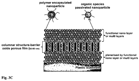
[0074] Figure 3C depicts yet another embodiment of a barrier stack according
to the
invention, deposited onto a planarized or non-planarized substrate that is of
plastic
material.
[0075] Figure 4 illustrates a qualitative test on barrier stack performance,
analysing
whether calcium degradation can occur (Type A).
[0076] Figure 5 illustrates a quantitative test on barrier stack performance,
analysing calcium degradation (Type B).
[0077] Figure 6 depicts a nanogetter layer coated polycarbonate substrate.
[0078] Figure 7 shows an SEM picture depicting the surface topography of
polymer
encapsulated nanoparticles at 20.000 x magnification.
[0079] Figure 8 shows an SEM picture depicting the surface topography of
polymer
encapsulated nanoparticles at 45.000 x magnification.
[0080] Figure 9 shows an SEM picture of plain anodise with 200nm pinholes
before coating at 10,000x magnification.
[0081] Figure 10 shows an SEM picture of encapsulated nanoparticles coated (4
micron coating thickness) onto the anodise (as shown in Fig. 9) in cross
section at
13,000 x magnification.
[0082] Figure 11 depicts an SEM picture of the bottom side of anodise , which
was
coated with a layer of polymer encapsulated nanoparticles shown-at a
magnification of
10,000. The disk was peeled off from the plastic substrate, thus showing the
defects
sealing mechanism.
[0083] Figure 12 shows a TEM image illustrating that the nanoparticles are
distributed in the polymer layer/film (50nm scale).
[0084] Figure 13A shows a SEM image of the distribution of aluminum oxide
nanoparticles in a polymer matrix as known in the art at 35.000 x
magnification. Figure
13B shows a SEM image of prior art aluminium oxide nanoparticles before
encapsulation
at 70.000 x magnification. Figure 13C shows a SEM image of the polymer
encapsulated
CA 02852879 2014-04-17
WO 2013/062486 PCT/SG2012/000402
24
nanoparticles of the invention at 100.000 x magnification and Figure 13D shown
a SEM
image of a layer of polymer encapsulated nanoparticles.
[0085] Figure 14A and Figure 14B depict the results of a standard test method
for
peel resistance. The ASTM peel test optical images show no delamination of the
polymer
encapsulated nanoparticle layer - aluminium oxide ¨ interfaces.
[0086] Figure 15 shows an illustration of polymer encapsulated nanoparticles
and
with polymer passivated particles as used in the invention, with Figures 15A
and 15B
showing a partially encapsulated (i.e. a passivated) nanoparticle and Figure
15C showing
a completely encapsulated nanoparticle.
[0087] Figure 16A and Figure 16B show SEM images of a cross section of a
barrier stack of the invention at 50.000 x magnification having a sealing
layer of polymer
encapsulated nanoparticles, deposited on an oxide layer which in turn is
arranged on a
PET plastic substrate.
[0088] Figure 17 shows a SEM image of a cross section of a barrier stack of
the
invention at 30.000 x magnification having a sealing layer of polymer
encapsulated
nanoparticles, deposited on an oxide layer which in turn is arranged on a PET
plastic
substrate.
DETAILED DESCRIPTION OF THE INVENTION
[0089] FIG. 3C shows one embodiment of an encapsulation barrier stack
according
to the invention, which is in addition arranged on a plastic substrate. The
encapsulation
barrier stack comprises a multilayer film. The multilayer film comprises one
or more
barrier layers and one or more sealing layers. The multilayer film may for
example include
one, two, three, four, five, six, seven, eight nine or ten barrier layers. The
multilayer film
may for example include one, two, three, four, five, six, seven, eight nine or
ten sealing
layers. In embodiments with a plurality of barrier layers and sealing layers
individual
barrier layers and sealing layers may be in contact with other barrier layers
and/or sealing
layers. In some embodiments an individual barrier layer is in contact with two
further
barrier layers. In some embodiments an individual barrier layer is in contact
with two
sealing layers. In some embodiments an individual barrier layer is in contact
with one
further barrier layer and one sealing layer. In some embodiments an individual
sealing
layer is in contact with two further sealing layers. In some embodiments an
individual
CA 02852879 2014-04-17
WO 2013/062486 PCT/SG2012/000402
sealing layer is in contact with two barrier layers. In some embodiments an
individual
sealing layer is in contact with one further sealing layer and one barrier
layer. In some
embodiments two or more sealing layers and one or more barrier layer(s) of the
multilayer
film are arranged in an alternating manner. In some embodiments the multilayer
film
5 includes a plurality of sealing layers and barrier layers arranged in an
alternating
sequence. In the embodiment depicted in Fig. 3C one barrier layer is present,
denominated the barrier oxide. In the embodiment depicted in Fig. 3C two
sealing layers
are present, each denominated a functional nano layer. As noted above, it is
also the
scope of the present invention that each barrier layer has a different number
of sealing
10 layers arranged thereon. In it also in the scope of the invention that
in case of a barrier
stack with more than one sealing layers, only the sealing layer that directly
contacts the
barrier layer comprises or consists of polymer encapsulated nanoparticles of
the invention
and that other layers can be a sealing layer of the prior art, for example, a
sealing layer as
described in WO 2008/057045 in which reactive nanoparticles are distributed in
a polymer
15 matrix. The barrier layers have low permeability to oxygen and/or
moisture. It will be
noted that barrier layers contain pinhole defects which extend through the
thickness of the
barrier layer. Pinhole defects along with other types of structural defects
limit the barrier
performance of barrier layers as oxygen and water vapour can permeate into the
barrier
layer via these defects, eventually traversing the encapsulation barrier stack
and coming
20 into contact with the oxygen/moisture sensitive device.
[0090] The sealing layer(s) comprise(s) reactive nanoparticles capable of
interacting
with water vapour and/or oxygen, thereby retarding the permeation of
oxygen/moisture
through the encapsulation barrier stack. In accordance with the present
invention, these
defects are at least partially covered up, or in some embodiments, entirely
filled up by the
25 nanoparticles in the sealing layer. The nanoparticles are polymer
encapsulated.
Examples of suitable polymers include, but are not limited to, polypropylene,
polyisoprene, polystyrene, polyvinyl chloride, polyisobutylene, polyethylene
terephthalate
(PET), polyacrylates (e.g. polymethyl-methacrylate (PMMA)), ethylene-vinyl
acetate
(EVA) copolymers, phenol formaldehyde resins, epoxy resins, poly(N-
propargylamides),
poly(0-propargylesters), and polysiloxanes.
[0091] The monomer or the pre-polymer that is used for the encapsulation of
the
reactive nanoparticles (and that is typically included in a non-aqueous based
discontinuous phase solution for the preparation of the sealing layer) may be
selected
from any suitable hydrophobic material. Illustrative examples of hydrophobic
monomers
CA 02852879 2014-04-17
WO 2013/062486 PCT/SG2012/000402
26
include, but are not limited to, styrenes (e.g., styrene, methylstyrene,
vinylstyrene,
dimethylstyrene, chlorostryene, dichlorostyrene, tert-butylstyrene,
bromostyrene, and p-
chloromethylstyrene), monofunctional acrylic esters (e.g., methyl acrylate,
ethyl acrylate,
isopropyl acrylate, n-butyl acrylate, butoxyethyl acrylate, isobutyl acrylate,
n-amyl
acrylate, isoamyl acrylate, n-hexyl acrylate, octyl acrylate, decyl acrylate,
dodecyl
acrylate, octadecyl acrylate, benzyl acrylate, phenyl acrylate, phenoxyethyl
acrylate,
cyclohexyl acrylate, dicyclopentanyl acrylate,
dicyclopentenyl acrylate,
dicyclopentenyloxyethyl acrylate, tetrahydrofurfuryl acrylate, isobornyl
acrylate, isoamyl
acrylate, lauryl acrylate, stearyl acrylate, benhenyl acrylate,
ethoxydiethylene glycol
acrylate, methoxytriethylene glycol acrylate, methoxydipropylene glycol
acrylate,
phenoxypolyethylene glycol acrylate, nonylphenol EO adduct acrylate, isooctyl
acrylate,
isomyristyl acrylate, isostearyl acrylate, 2-ethylhexyl diglycol acrylate, and
oxtoxypolyethylene glycol polypropylene glycol monoacrylate), monofunctional
methacrylic esters (e.g., methyl methacrylate, ethyl methacrylate, isopropyl
methacrylate,
n-butyl methacrylate, i-butyl methacrylate, tert-butyl methacrylate, n-amyl
methacrylate,
isoamyl methacrylate, n-hexyl methacrylate, 2-ethylhexyl methacrylate, lauryl
methacrylate, tridecyl methacrylate, stearyl methacrylate, isodecyl
methacrylate, octyl
methacrylate, decyl methacrylate, dodecyl methacrylate, octadecyl
methacrylate,
methoxydiethylene glycol methacrylate, polypropylene glycol monomethacrylate,
benzyl
methacrylate, phenyl methacrylate, phenoxyethyl methacrylate, cyclohexyl
methacrylate,
tetrahYdrofurfuryl methacrylate, tert-butylcyclohexyl methacrylate, behenyl
methacrylate,
dicyclopentanyl methacrylate, dicyclopentenyloxyethyl methacrylate, and
polypropylene
glycol monomethacrylate), ally) compounds (e.g., allylbenzene, allyI-3-
cyclohexane
propionate, 1-allyI-3,4-dimethoxybenzene, ally) phenoxyacetate, ally'
phenylacetate,
allylcyclohexane, and ally) polyvalent carboxylate), unsaturated esters of
fumaric acid,
maleic acid, itaconic acid, etc., and radical polymerizable group-containing
monomers
(e.g., N-substitued maleimide and cyclic olefins).
[0092] In one embodiment, the polymer-encapsulated nanoparticles may be formed
in a non-water-based solution (sealing mixture). In this embodiment, the
monomers may
be selected from acid containing radical polymerizable monomers.
[0093] In another embodiment, the polymer-encapsulated nanoparticles may be
formed in the sealing mixture of an acid containing radical polymerizable
monomers. In
this embodiment, the monomer may be selected from acrylic acid, methacrylic
acid,
acrylamides, methacrylamides, hydroxyethyl-methacrylates, ethylene-oxide-base
CA 02852879 2014-04-17
WO 2013/062486 PCT/SG2012/000402
27
methacrylates, and combinations thereof.
[0094] In another embodiment, the polymer-encapsulated nanoparticle may be
formed in a sealing mixture wherein pre-polymers are used. Such pre-polymers
might be
selected from an acrylic oligomer having a molecular weight less than about
1000 Da and
a viscosity less than about 300 cPoise.
[0095] In some embodiments the one or more sealing layer(s) at least
essentially
consist(s) of the polymer encapsulated reactive nanoparticles. The term "at
least
essentially consisting of" means that the respective layer is generally free
of other matter,
as judged by standard analytical techniques. The layer may contain minor
amounts of
other matter, but it may also be entirely free of other matter, at least as
judged by known
analytical techniques. Thus, the one or more sealing layer(s) may consist(s)
only of the
polymer encapsulated reactive nanoparticles. A portion of the plurality of
polymer
encapsulated nanoparticles or all polymer encapsulated nanoparticles may have
an
aliphatic, alicyclic, aromatic or arylaliphatic compound immobilized thereon.
The aliphatic,
alicyclic, aromatic or arylaliphatic compounds have a polar group. The polar
group may,
for example, be a hydroxyl group, a carboxyl group, a carbonyl group, an amino
group, an
amido group, a thio group, a seleno group, and a telluro group.
[0096] The term "aliphatic" means, unless otherwise stated, a straight or
branched
hydrocarbon chain, which may be saturated or mono- or poly-unsaturated and
include
heteroatoms (see below). An unsaturated aliphatic group contains one or more
double
and/or triple bonds (alkenyl or alkinyl moieties). The branches of the
hydrocarbon chain
may include linear chains as well as non-aromatic cyclic elements. The
hydrocarbon
chain, which may, unless otherwise stated, be of any length, and contain any
number of
branches. Typically, the hydrocarbon (main) chain includes 1 to 5, to 10, to
15 or to 20
carbon atoms. Examples of alkenyl radicals are straight-chain or branched
hydrocarbon
radicals which contain one or more double bonds. Alkenyl radicals normally
contain about
two to about twenty carbon atoms and one or more, for instance two, double
bonds, such
as about two to about ten carbon atoms, and one double bond. Alkynyl radicals
normally
contain about two to about twenty carbon atoms and one or more, for example
two, triple
bonds, such as two to ten carbon atoms, and one triple bond. Examples of
alkynyl
radicals are straight-chain or branched hydrocarbon radicals which contain one
or more
triple bonds. Examples of alkyl groups are methyl, ethyl, propyl, butyl,
pentyl, hexyl, heptyl,
octyl, nonyl, decyl, the n isomers of these radicals, isopropyl, isobutyl,
isopentyl, sec-butyl,
tert-butyl, neopentyl, 3,3-dimethylbutyl. Both the main chain as well as the
branches may
CA 02852879 2014-04-17
WO 2013/062486 PCT/SG2012/000402
28
furthermore contain heteroatoms as for instance N, 0, S, Se or Si or carbon
atoms may
be replaced by these heteroatoms.
[0097] The term "alicyclic" means, unless otherwise stated, a non-aromatic
cyclic
moiety (e.g. hydrocarbon moiety), which may be saturated or mono-or poly-
unsaturated.
.. The cyclic hydrocarbon moiety may also include fused cyclic ring systems
such as decalin
and may also be substituted with non-aromatic cyclic as well as chain
elements. The main
chain of the cyclic hydrocarbon moiety may, unless otherwise stated, be of any
length and
contain any number of non-aromatic cyclic and chain elements. Typically, the
hydrocarbon (main) chain includes 3, 4, 5, 6, 7 or 8 main chain atoms in one
cycle.
.. Examples of such moieties include, but are not limited to, cylcopentyl,
cyclohexyl,
cycloheptyl, or cyclooctyl. Both the cyclic hydrocarbon moiety and, if
present, any cyclic
and chain substituents may furthermore contain heteroatoms, as for instance N,
0, S, Se
or Si, or a carbon atom may be replaced by these heteroatoms. The term
"alicyclic" also
includes cycloalkenyl moieties that are unsaturated cyclic hydrocarbons, which
generally
.. contain about three to about eight ring carbon atoms, for example five or
six ring carbon
atoms. Cycloalkenyl radicals typically have a double bond in the respective
ring system.
Cycloalkenyl radicals may in turn be substituted.
[0098] The term "aromatic" means, unless otherwise stated, a planar cyclic
hydrocarbon moiety of conjugated double bonds, which may be a single ring or
include
.. multiple fuse,d or covalently linked rings, for example, 2, 3 or 4 fysed
rings. The term
aromatic also includes alkylaryl. Typically, the hydrocarbon (main) chain
includes 5, 6, 7
or 8 main chain atoms in one cycle. Examples of such moieties include, but are
not
limited to, cylcopentadienyl, phenyl, napthalenyl-, [10]annulenyl-(1,3,5,7,9-
cyclodeca-
pentaenyl-), [12]annulenyl-, [8]annulenyl-, phenalene (perinaphthene), 1,9-
dihydropy-
.. rene, chrysene (1,2-benzophenanthrene). An example of an alkylaryl moiety
is benzyl.
The main chain of the cyclic hydrocarbon moiety may, unless otherwise stated,
be of any
length and contain any number of heteroatoms, as for instance N, 0 and S.
Examples of
such heteroarom containing moieties (which are known to the person skilled in
the art)
include, but are not limited to, furanyl-, thiophenyl-, naphtyl-,
naphthofuranyl-, anthrax-
thiophenyl-, pyridinyl-, pyrrolyl-, quinolinyl, naphthoquinolinyl-,
quinoxalinyl-, indolyl-,
benzindolyl-, imidazolyl-, oxazolyl-, oxoninyl-, oxepinyl-, benzoxepinyl-,
azepinyl-,
thiepinyl-, selenepinyl-, thioninyl-, azecinyl- (azacyclodecapentaenyl-),
diazecinyl-,
azacyclododeca-1,3,5,7,9,11-hexaene-5,9-diy1-, azozinyl-, diazocinyl-,
benzazocinyl-,
azecinyl-, azaundecinyl-, thia[11]annulenyl-, oxacyclotrideca-2,4,6,8,10,12-
hexaenyl- or
CA 02852879 2014-04-17
WO 2013/062486 PCT/SG2012/000402
29
triazaanthracenyl-moieties.
[0099] By the term "arylaliphatic" is meant a hydrocarbon moiety, in which one
or
more aromatic moieties are substituted with one or more aliphatic groups. Thus
the term
"arylaliphatic" also includes hydrocarbon moieties, in which two or more aryl
groups are
connected via one or more aliphatic chain or chains of any length, for
instance a
methylene group. Typically, the hydrocarbon (main) chain includes 5, 6, 7 or 8
main chain
atoms in each ring of the aromatic moiety. Examples of arylaliphatic moieties
include, but
are not limited, to 1-ethyl-naphthalene, 1,1'-methylenebis-benzene, 9-
isopropylanthrax-
cene, 1,2, 3-trimethyl-benzene, 4-
pheny1-2-buten-1-ol, 7-chloro-3-(1-methylethyl)-
quinoline, 3-heptyl-furan, 642-(2,5-diethylphenypethy1]-4-ethyl-quinazoline
or, 7,8-dibuty1-
5,6-diethyl-isoquinoline.
[00100] Each of the terms "aliphatic", "alicyclic", "aromatic" and
"arylaliphatic" as
used herein is meant to include both substituted and unsubstituted forms of
the respective
moiety. Substituents my be any functional group, as for example, but not
limited to,
amino, amido, azido, carbonyl, carboxyl, cyano, isocyano, dithiane, halogen,
hydroxyl,
nitro, organometal, organoboron, seleno, silyl, silano, sulfonyl, thio,
thiocyano,
trifluoromethyl sulfonyl, p-toluenesulfonyl, bromobenzenesulfonyl,
nitrobenzenesulfonyl,
and methane-sulfonyl.
[00101] In some embodiments the at least one sealing layer conforms
substantially
to the shape of the. defects present on the surface of the at least one
barrier layer. The
sealing layer may act as a planarising material that smoothens the surface of
the
substrate, thereby covering defects on the substrate which could provide
pathways for the
infiltration of moisture/oxygen. In this regard, application of a sealing
layer above a barrier
layer may further allow smoothening the surface in case further barrier layers
are
intended to be deposited on the barrier film.
[00102] The preceding embodiments relate to an encapsulation barrier stack in
which the multilayer film is immobilized, e.g. laminated onto only one side of
a substrate.
In some embodiments a barrier stack is immobilized on a double-laminated
substrate in
which a multilayer film is laminated or deposited on to two sides, which may
be opposing
sides, of a base substrate. An encapsulation barrier stack may for instance
include a
substrate that is sandwiched between two multilayer films.
[00103] As will be apparent from the above, a multilayer film according to the
invention has at least two layers, a barrier layer and a sealing layer, each
of which has an
CA 02852879 2014-04-17
WO 2013/062486 PCT/SG2012/000402
upper face and a lower face, defining a plane. Each layer further has a
circumferential
wall defining a thickness of the layer. Typically each layer is of at least
essentially uniform
thickness. In some embodiments the circumference of each layer is of at least
essentially
the same dimensions as the circumference of any other layer. A multilayer film
according
5 to the
invention has two (upper and lower) outer surfaces defined by the upper face
of a
first layer and the lower face of a second layer. These two surfaces are
arranged on at
least essentially opposing sides of the multilayer film. Each of these two
surfaces defines
a plane. In typical embodiments these two planes are essentially parallel to
each other.
Furthermore these two surfaces are exposed to the ambience. Typically one or
both of
10 these
planes is/are adapted for being contacted with the surface of a substrate,
including
for being immobilized thereon. In some embodiments the surface topology of the
respective surface of the multilayer film is at least essentially matching,
e.g. at least
essentially congruent to, the surface topology of the plane of the substrate.
[00104] The encapsulation barrier stack of the invention can be used in
several
15 ways
for encapsulating a moisture and oxygen sensitive device. Any device may be
encapsulated by an encapsulation barrier stack of the invention, such as an
OLED,
pharmaceutical drugs, jewellery, reactive metals, electronic components or
food
substances. For example, it can be arranged, for example laminated or
deposited, onto a
conventional polymer substrate that is used to support the OLED. As explained
above,
20 pinhole defects in the barrier layer are sealed by the polymer encapsulated
nanoparticulate material of the sealing layer. The OLED may be arranged
directly on the
multilayer film, and for instance encapsulated under a cover such as a glass
cover, for
instance using rim sealing or thin-film encapsulation comprising the
attachment of an
encapsulation barrier stack over the OLED, hereinafter referred to as
'proximal
25
encapsulation', is also possible. Proximal encapsulation is in particular
suitable for flexible
OLED devices. In such an embodiment the multilayer film of the encapsulation
barrier
stack conforms to the external shape of the OLED device.
[00105] An encapsulation barrier stack according to the invention may be
produced
by forming on one or more barrier layer(s), on a substrate or on a (further)
sealing layer, a
30
sealing layer. In some embodiments the sealing layer may be formed on a
substrate. The
sealing layer may be formed by mixing a polymerisable compound with a
plurality of
reactive nanoparticles as defined above. The plurality of nanoparticles may in
some
embodiments be a colloidal dispersion comprising nanoparticles dispersed in a
suitable
liquid such as an organic solvent. In some embodiments a polar solvent such as
e.g.
CA 02852879 2014-04-17
WO 2013/062486 PCT/SG2012/000402
31
ethanol, acetone, N,N-dimethyl-formamide, isopropanol, ethyl acetate or
nitromethane, or
a non-polar organic solvent such as e.g. benzene, hexane, dioxane,
tetrahydrofuran or
diethyl ether (cf. also below). As explained above, in order to allow for
encapsulation of
the reactive nanoparticles, the polymerisable compound (which might be a
monomeric
compound) is present in such a low concentration in the sealing mixture that
the
polymerisable compound is adsorbed on the surface of the reactive particles,
thereby
coating the particles and avoiding formation of a (bulk) matrix that
incorporates the entire
reactive particles.
[00106] Often liquids are classified into polar and non-polar liquids in order
to
characterize properties such as solubility and miscibility with other liquids.
Polar liquids
typically contain molecules with an uneven distribution of electron density.
The same
classification may be applied to gases. The polarity of a molecule is
reflected by its
dielectric constant or its dipole moment. Polar molecules are typically
further classified
into protic and non-protic (or aprotic) molecules. A fluid, e.g. a liquid,
that contains to a
large extent polar protic molecules may therefore be termed a polar protic
fluid. A fluid,
e.g. a liquid, that contains to a large extent polar non-protic molecules may
be termed a
polar non-protic fluid. Protic molecules contain a hydrogen atom which may be
an acidic
hydrogen when the molecule is dissolved for instance in water or an alcohol.
Aprotic
molecules do not contain such hydrogen atoms.
[00107] Examples of non-polar liquids include, but are not limited to, hexang,
heptane, cyclohexane, benzene, toluene, dichloromethane, carbon tetrachloride,
carbon
disulfide, dioxane, diethyl ether, or diisopropylether. Examples of dipolar
aprotic liquids
are methyl ethyl ketone, chloroform, tetrahydrofuran, ethylene glycol
monobutyl ether,
pyridine, methyl isobutyl ketone, acetone, cyclohexanone, ethyl acetate,
isobutyl
isobutyrate, ethylene glycol diacetate, dimethylformamide, acetonitrile, N,N-
dimethyl
acetamide, nitromethane, acetonitrile, N-methylpyrrolidone, methanol, ethanol,
propanol,
isopropanol, butanol, N,N-diisopropylethylamine, and dimethylsulfoxide.
Examples of
polar protic liquids are water, methanol, isopropanol, tert.-butyl alcohol,
formic acid,
hydrochloric acid, sulfuric acid, acetic acid, trifluoroacetic acid,
dimethylarsinic acid
[(CH3)2AsO(OH)], acetonitrile, phenol or chlorophenol. Ionic liquids typically
have an
organic cation and an anion that may be either organic or inorganic. The
polarity of ionic
liquids (cf. below for examples) is known to be largely determined by the
associated
anion. While e.g. halides, pseudohalides, BF4-, methyl sulphate, NO3-, or CI04-
are polar
liquids, hexafluorophosphates, AsF6-, bis(perfluoroalkyl)-imides, and [c4F6so3-
are non-
CA 02852879 2014-04-17
WO 2013/062486 PCT/SG2012/000402
32
polar liquids.
[00108] The mixing of the polymerisable compound with the plurality of
nanoparticles may in some embodiments be carried out in a polar organic
solvent such as
defined above. In one embodiment the polar organic solvent includes a mixture
of
isopropanol and ethyl acetate, for example in a molar ratio from about 2 : 1
to about 1 :
10, e.g. about 1:1, about 1 : 2, about 1 : 3, about 1 : 5 or about 1 : 10. The
mixture of the
polymerisable compound and the reactive nanoparticles may be applied onto the
barrier
layer, and the polymerisable compound may be polymerised to form a polymer.
Polymerisation is allowed to occur under conditions that allow the
nanoparticles to be
encapsulated by the polymer formed, i.e. using a low concentration of the
polymerisable
compound and, for example, additionally subjecting the sealing mixture to
sonification.
The sealing solution may be web flight coated onto the barrier layer, for
example, via a
roll-to-roll process. The coating of barrier layer and sealing layer is
repeated for a
predetermined number of times to obtain a multilayer film with a desired
barrier property.
For example, a multilayer film comprising 5 paired layers may be obtained by
oxide
coating and web flight coating to be repeated 5 times to form 5 paired layer.
[00109] In some embodiments a surfactant is added to the mixture of the
polymerisable compound and the plurality of nanoparticles. Numerous
surfactants, which
are partly hydrophilic and partly lipophilic, are used in the art, such as for
instance alkyl
benzene sulfonates, alkyl phenoxy polyethoxy ethanols, alkyl glucosides,
secondary and ,
tertiary amines such as diethanolamine, TWeen, Triton 100 and triethanolamine,
or e.g.
fluorosurfactants such as ZONYL FSO-100 (DuPont). A surfactant may for
instance be
a hydrocarbon compound, a hydroperfluoro carbon compound or a perfluorocarbon
compound. It may for example be substituted by a sulfonic acid, a
sulphonamide, a
carboxylic acid, a carboxylic acid amide, a phosphate, or a hydroxyl group.
Examples of a
hydrocarbon based surfactant include, but are not limted to, sodium dodecyl
sulfate, cetyl
trimethyl-ammonium bromide, an alkylpolyethylene ether, dodecyldimethyl (3-
sulfopropyl)
ammonium hydroxide (C12N3S03), hexadecyldimethyl (3-sulfopropyl) ammonium
hydroxide (C16N3S03), coco (amidopropyl)hydroxyl
dimethylsulfobetaine
(RCONH(CH2)3N+(CH3)2CH2CH(OH)CH2S03- with R=C8¨C18), cholic acid, deoxycholic
acid, octyl glucoside, dodecyl maltoside, sodium taurocholate, or a polymer
surfactant
such as e.g. Supelcoat PS2 (Supelco, Bellefonte, PA, USA), methylcellulose,
hydroxy-
propylcellulose, hydroxyethylcellulose, or hydroxypropylmethylcellulose. The
surfactant
may for instance be a hydrocarbon compound, a hydroperfluoro carbon compound
or a
CA 02852879 2014-04-17
WO 2013/062486 PCT/SG2012/000402
33
perfluorocarbon compound (supra), which is substituted by a moiety selected
from the
group consisting of a sulfonic acid, a sulphonamide, a carboxylic acid, a
carboxylic acid
amide, a phosphate, or a hydroxyl group.
[00110] Examples of perfluorocarbon-surfactants include, but are not limited
to,
pentadecafluorooctanoic acid, heptadecafluorononanoic acid,
tridecafluoroheptanoic acid,
undecafluorohexanoic acid, 1,
1,1,2,4,4,5,5,6,6, 7,7,8, 8,9,9, 10,10,11, 11, 11-heneicosa-
fl uoro-3-oxo-2-undecanesulfonic acid, 1, 1,2,2, 3, 3,4 ,4,5,5,6, 6, 6-
tridecafluoro-1-hexane-
sulfonic acid, 2,2,3,3,4,4,5,5-octafluoro-5-[(tridecafluorohexyl)oxy]-
pentanoic acid, 2,2,3,3-
tetrafluoro-3-[(tridecafluorohexyl)oxy]-propanoic acid], N,N'-
[phosphinicobis(oxy-2,1-
ethanediyI)]bis[1, 1,2,2, 3,3,4,4,5,5,6,6, 7, 7,8,8,8-heptadecafluoro-N-propy1-
1-octanesulfon-
amide, 1,1,2,2,3,3,4,4,5,5,6,
6,7,7,8,8,8-heptadecafluoro-1-octanesulfonic acid,
1,1,2,2,3,3,4,4,5,5,6,6,7,7,8,8,8-heptadecafluoro-1-octanesulfonyl
fluoride, 203-D-
galactopyranosyloxy)methy1]-2-[(1-oxo-2-propenyl)amino]-1,3-propanediy1
carbamic acid
(3,3,4,4,5,5,6,6,7,7,8, 8,8-tridecafluorooctyI)-ester, 6-
(3,3,4,4,5,5,6,6,7,7,8,8,8-tridecafluo-
rooctyl hydrogen phosphate)-D-glucose, 3-
(3,3,4,4,5,5, 6,6,7,7,8,8,9,9, 10, 10, 10-
heptadecafluorodecyl hydrogen phosphate)-D-glucose,
2-(perfluorohexyl)ethyl
isocyanate, 2,2,3,3,4,4,5,5,6,6,7,7,8,8,8-pentadecafluoro-N-phenyl-octanamide,
1,1,2,2,3,
3,4,4,5,5,6,6,7,7,8,8,9,9, 10,10,11, 11, 12,12,12-pentacosafluoro-N-(2-
hydroxyethyl)-N-
propy1-1-dodecanesulfonamide, 2-methyl-,2-
[[(heptadecafluorooctyl)sulfonyl]methylami-
no]-2-propenoic acid ethyl ester, 3-4(2,2,3,3,4,4, 5,5,6,6,7,7,8,8,8-
pentadecafluoro-1-
oxooctyI)-benzenesulfonic acid, 3-(heptadecafluorooctyI)-benzenesulfonic acid,
4-
[(2,2,3,3,4,4,5,5,6,6,7,7,8,8,8-pentadecafluoro-1-oxooctyl)amino]-
benzenesulfonic acid, 3-
[(o-perfluorooctanoyl)phenoxy]propanesulfonic acid, N-ethy1-1,1,2,2,2-
pentafluoro-N-(26-
hydroxy-3,6,9, 12,15,18,21, 24-octaoxahexacos-1-yI)-ethanesulfonamide, 3-
[ethyl[(hepta-
decafluorooctyl)sulfonyl]amino]-1-propanesulfonic acid, 1,2,2,3,3, 4,5,5,6,6-
decafluoro-4-
(pentafluoroethyl)-cyclohexanesulfonic acid, 2-[1-
[difluoro(pentafluoroethoxy)methy1]-
1,2,2,2-tetrafluoroethoxy]-1,1,2,2-tetrafluoro-ethanesulfonic acid, N-[3-
(dimethyloxido-
amino)propy1]-2,2,3,3,4,4-hexafluoro-4-(heptafluoropropoxy)-butanamide, N-
ethyl-N-
[(heptadecafluorooctyl)sulfonyI]-glycine, or 2,3,3,3-tetrafluoro-2-
[1,1,2,3,3,3-hexafluoro-2-
[(tridecafluorohexyl)oxy]propoxy]-1-propanol, to name a few.
[00111] Examples of perfluorocarbon-surfactants also include polymeric
compounds such as a-[2-[bis(heptafluoropropyl)amino]-2-fluoro-1-
(trifluoromethyl)-
ethenyl]-(0-[[2-[bis(heptafluoropropyl)amino]-2-fluoro-1-
(trifluoromethyl)ethenyl]oxyFpoly-
(oxy-1,2-ethanediy1),
a42-[[(nonacosafluorotetradecyl)sulfonyl]propylamino]ethy1]-(.0-
CA 02852879 2014-04-17
WO 2013/062486 PCT/SG2012/000402
34
hydroxy-poly(oxy-1,2-ethanediy1), polyethylene glycol diperfluorodecyl ether,
a-[2-[ethyl-
[(heptadecafluorooctyl)sulfonyl]aminoiethy1]-(0-hydroxy-poly(oxy-1,2-
ethanediy1), a42-
[ethyl[(pentacosafluorododecypsulfonyliamino]ethyl]-(0-hydroxy-poly(oxy-1,2-
ethanediy1),
a[2-[[(heptadecafluorooctyl)sulfonyl]propylaminoiethyl]- a-hydroxy-poly(oxy-
1,2-
ethanediyl), N-(2, 3-dihydroxypropy1)-2,2-difluoro-2-[1,1,2,2-tetrafluoro-2-
[(tridecafluorohexyl)oxy]ethoxyFacetamide, a-
(2-carboxyethyl)-(0-
[[(tridecafluorohexyl)oxy]methoxyl-poly(oxy-1,2-ethanediy1),a-[2,3,3,3-
tetrafluoro-241,1,2,
3,3, 3-hexafluoro-2-(heptafluoropropoxy)propoxy]-1-oxopropyli-co-hydroxy-
poly(oxy-1,2-
ethanediyl), and 2,3,3,3-tetrafluoro-2-(heptafluoropropoxy)-propionic acid
polymer.
[00112] In some embodiments a surface modifying compound such as a silane is
added to the sealing mixture. Examples of suitable silanes include acetoxy,
alkyl, amino,
amino/alkyl, aryl, diamino, epoxy, fluroalkyl, glycol, mercapto, methacryl,
silicic acid ester,
silyl, ureido, yinyl, and vinyl/alkyl silanes.
[00113] Illustrative examples of such silanes include, but are not limited to,
di-tert-
butoxydiacet-oxysilane, hexadecyltrimeth-oxysilane, alkylsiloxane, Bis(3-
triethoxysilyl-
propyl) amine, 3-aminopropyl-methyldiethoxysilane, triamino-functional
propyltrimethoxy-
silane, phenyltrimethoxysilane, phenyltriethoxysilane, 2-aminoethy1-3-amino-
propylmethyl,
dimethoxysilane, 2-aminoethy1-3-amino-propyl, trimethoxysilane, proprietary
aminosilane
composition, 3-glycidyloxy, propyltriethoxysilane, tridecafluoroocty-
ltriethoxysilane,
polyether-functional trimethoxysilane, 3-mercaptopropyltri-methoxysilane, 3-
methacryloxypropyl-trimethoxysilane, ethyl polysilicate, tetra-n-propyl
orthosilicate,
hexamethyl-disilazane, vinyltrichlorosilane,
vinyltrimethoxysilane, vinyl-functional
oligosiloxane, 3-methacryloxypropyltrimethoxysilane and combinations thereof.
[00114] In some embodiments forming the sealing layer is carried out under an
inert
atmosphere, which may for example include or consist of nitrogen, argon, neon,
helium,
and/or sulfur hexafluoride (SF6)-
[00115] Forming the one or more barrier layer(s) may be achieved by any
suitable
deposition method such as spin coating, flame hydrolysis deposition (FHD),
slot die
coating, curtain gravure coating, knife coating, dip coating, plasma
polymerisation or a
chemical vapour deposition (CVD) method. Examples of CVD methods include, but
are
not limited to plasma enhanced chemical vapor deposition (PECVD) or inductive
coupled
plasma enhanced chemical vapor deposition (ICP-CVD).
[00116] In one embodiment the barrier layer is deposited onto a further layer
such
CA 02852879 2014-04-17
WO 2013/062486 PCT/SG2012/000402
as a sealing layer or onto a substrate using sputtering techniques known in
the art.
Sputtering is a physical process of depositing a thin film by controllably
transferring atoms
from a source to a substrate, which is known in the art. The substrate is
placed in a
vacuum chamber (reaction chamber) with the source material, named a target,
and an .
5 inert
working gas (such as argon) is introduced at low pressure. A gas plasma is
struck in
radio frequency (RF) or direct current (DC) glow (ejection of secondary
electrons)
discharged in the inter gas, which causes the gas to become ionized. The ions
formed
during this process are accelerated towards the surface of the target, causing
atoms of
the source material to break off from the target in vapour form and condense
on the
10 substrate. Besides RF and DC sputtering, magnetron sputtering is known as
third
sputtering technique. For magnetron sputtering, DC, pulsed DC, AC and RF power
supplies can be used, depending upon target material, if reactive sputtering
is desired
and other factors. Plasma confinement on the target surface is achieved by
locating a
permanent magnet structure behind the target surface. The resulting magnetic
field forms
15 a
closed-loop annular path acting as an electron trap that reshapes the
trajectories of the
secondary electrons ejected from target into a cycloidal path, greatly
increasing the
probability of ionization of the sputtering gas within the confinement zone.
Positively
charged argon ions from this plasma are accelerated toward the negatively
biased target
(cathode), resulting in material being sputtered from the target surface.
20 [0100]
Magnetron sputtering differentiates between balanced and unbalanced
magnetron sputtering. An "unbalanced" magnetron is simply a design where the
magnetic
flux from one pole of the magnets located behind the target is greatly unequal
to the other
while in a "balanced" magnetron the magnetic flux between the poles of the
magnet are
equal. Compared to balanced magnetron sputtering, unbalanced magnetron
sputtering
25
increases the substrate ion current and thus the density of the substrate
coating. In one
embodiment a sputtering technique such as RF sputtering, DC sputtering or
magnetron
sputtering is used to deposit the barrier layer onto the substrate layer. The
magnetron
sputtering can include balanced or unbalanced magnetron sputtering. In one
embodiment, the barrier layer is a sputtered barrier layer.
30 [0101]
The barrier stack may be applied onto a substrate, such as a polycarbonate
or a PET substrate. In some embodiments a barrier layer may be formed with the
aid of a
respective substrate. The substrate may be plasma treated and coated with
alumina
barrier material via magnetron sputtering, thereby forming a barrier layer.
[0102] In some embodiments a further material such as ITO may be deposited,
e.g.
CA 02852879 2014-04-17
WO 2013/062486 PCT/SG2012/000402
36
magnetron sputtered, over the multilayer film to form an ITO coating after the
multilayer
film has been formed. If the encapsulation barrier stack is to be used in
Passive Matrix
displays, only ITO lines are required instead of a complete coat of 10T. A
protective liner
is subsequently formed on the ITO coating. Any suitable material may be used,
depending on the intended purpose, e.g. scratch resistant films or glare
reduction films,
such as MgF/LiF films. After forming the protective film, the encapsulation
barrier stack is
packed in aluminium foil packaging or slit into predetermined dimensions for
assembly
with other components.
[0103] As one of ordinary skill in the art will readily appreciate from the
disclosure of
the present invention, other compositions of matter, means, uses, methods, or
steps,
presently existing or later to be developed that perform substantially the
same function or
achieve substantially the same result as the corresponding exemplary
embodiments
described herein may likewise be utilized according to the present invention.
EXEMPLARY EMBODIMENTS
[0104] Typical embodiments of a multi-layer barrier stack design of the
present
invention include a barrier oxide film deposited onto planarized or non-
planarized plastic
substrate (stretchable or non-stretchable). Functionalized single or multi-
layer nano-
materials are deposited on to barrier oxide films. For example, functionalized
nano-
particles consist of polymer-encapsulated nano-particles and/or functionalized
nanoparticle with organic species may be deposited on to a barrier oxide film
as a
functionalized nanoparticle layer. The functionalized nanoparticles can
penetrate into the
pores of the barrier oxide film and enhance the barrier properties. The
combination of
mutually chemically interconnected organic and inorganic nanoparticles results
in
coatings with very low permeability of gases. If polymer is encapsulated on to
the
nanoparticle, the ratio of polymer and nanoparticles by weight are preferably
1:4 or less,
1:5 or less, or 1:6 or less.
[0105] The functionalized nanoparticle layer (Nano-layer) can be a multi-
nanolayer.
These functionalized multi-nanolayers can act as a barrier layers and can also
act as a
UV blocking layer, anti-reflection layer, to enhance the mechanical
properties, which
includes adhesion, stretchability, weatherablity and optical properties.
[0106] For example, the first functionalized nanoparticle layer can be a
defect
sealing layer and anti-reflection layer and the second layer can be a UV
blocking layer
CA 02852879 2014-04-17
WO 2013/062486 PCT/SG2012/000402
37
and third layer may be a light extraction layer. Therefore, in one barrier
stack, the multi-
functional properties can be obtained.
[0107] In one embodiment, the defect-sealing layer(s) consist of polymer
encapsulated titanium nanoparticles, zinc nanoparticles, silica or hollow
silica particles.
These (polymer encapsulated) particles can be used to enhance the barrier
properties of
the stack, to block the UV light and have anti-reflection properties in the
visible region.
Functionalization Nanoparticles Layer or Multi-Nano layers
Substrate Materials
[0108] Polymers that may be used in the base substrate in the present
invention
include both organic and inorganic polymers. Examples of organic polymers
which are
suitable for forming the base substrate include both high and low permeability
polymers
such as cellophane, poly(1-trimethylsilyI-1-propyne, poly(4-methyl-2-pentyne),
polyimide,
polycarbonate, polyethylene, polyethersulfone, epoxy resins, polyethylene
terephthalate
(PET), polystyrene, polyurethane, polyacrylate, and polydimethylphenylene
oxide.
Microporous and macroporous polymers such as styrene-divinylbenzene
copolymersõ
polyvinylidene fluoride (PVDF), nylon, nitrocellulose, cellulose or acetate
may also be
used. Examples of inorganic polymers which are suitable in the present
invention include
silica (glass), nano-clays, silicones, polydimethylsiloxanes,
biscyclopentadienyl iron,
polyphosphazenes and derivatives thereof. The base substrate may also include
or
consist of a mixture or a combination of organic and/or inorganic polymers.
These
polymers can be transparent, semi-transparent or completely opaque.
Surface Preparation
[0109] The barrier stacks or glass substrates are rinsed with isopropyl
alcohol (IPA)
and blow-dried with nitrogen. These processes help to remove macro scale
adsorbed
particles on the surface. Acetone and methanol cleaning or rinsing is not
recommended.
After nitrogen blow-dry, the substrates are placed in the vacuum oven, with
the pressure
of 10-1mbar, for degassing absorbed moisture or oxygen. The vacuum oven is
equipped
with fore line traps to prevent hydrocarbon oil back migrating from vacuum
pump to the
vacuum oven. Immediately after the degassing process, the barrier stacks are
transferred
to the plasma treatment chamber (e.g. ULVAC SOLCIET Cluster Tool). RF argon
plasma
is used to bombard the surface of the barrier film with low energy ions in
order to remove
CA 02852879 2014-04-17
WO 2013/062486 PCT/SG2012/000402
38
surface contaminants. The base pressure in the chamber was maintained below 4
x 10-6
mbar. The argon flow rate is 70sccm. The RF power is set at 200 W and an
optimal
treatment time usually 5 to 8 minutes is used depending on the surface
condition.
Inorganic barrier oxide films fabrication
[0110] The sputtering technique, EB evaporation and Plasma Enhanced Physical
Vapor deposition methods were used to deposit the metal oxide barrier layer.
The
unbalanced magnetron sputter system is used to develop high-density oxide
barrier films.
In this sputtering technique, a metal layer of typically a few mono-layers
will be deposited
from an unbalanced magnetron and then oxygen will be introduced to the system
to
create oxygen plasma, directed towards the substrate to provide argon and
oxygen ion
bombardment for a high packing-density oxide film. This plasma will also
increase the
reactivity of the oxygen directed onto the growing film surface and provides
for more
desirable structures. In order to deposit dense films without introducing
excessive intrinsic
stresses, a high flux (greater than 2 mA/cm2) of low energy (-25 eV) oxygen
and argon
ions to bombard the growing barrier oxide films.
[0111] The continuous feedback control unit is used to control the reactive
sputtering processes. The light emitted by the sputtering metal in the intense
plasma of
the magnetron racetrack is one indicator of the metal sputtering rate and the
oxygen
partial pressure. This indication can be used to control the process and hence
achieve an
accurate oxide film stoichiometry. By using a continuous feedback control unit
from a
plasma emission monitor, reproducible films and desirable barrier properties
were
obtained. Various barrier layers including SIN, A1203, and Indium tin oxide
were prepared
by conventional and unbalanced magnetron sputtering techniques and tested the
single
barrier layer properties.
[0112] In addition, barrier oxide films (SiOx & A1203) were produced by EB
evaporation and Plasma enhanced physical vapor deposition methods at the speed
of
500 meters/min. Coating thickness is 60nm to 70nm.
Functionalized Nanoparticle Layer
[0113] The surface modification is a key aspect in the use of nanosized
materials
(also referred to as nanomaterials here). It is the surface that makes the
nanosized
materials significantly more useful than conventional non-nanomaterials. As
the size of
CA 02852879 2014-04-17
WO 2013/062486 PCT/SG2012/000402
39
the material decreases, its surface-to-volume ratio increases. This presents
considerable
advantage to modify properties of nanomaterials through surface
functionalization
techniques. The functionalized nanoparticles are inclusive of polymer
encapsulation on to
the nanoparticle and organic species passivated nanoparticles. The
functionalization
techniques, which includes non-covalent (physical) bond and covalent bond
(chemical)
that can be applied to the nanoparticles. There are several methods available.
Ultrasonic
cavitation can be used to disperse nano-sized particles into solvent.
[0114] Covalent functionalization has been widely investigated and has
produced an
array of modified nanomaterial bearing small molecules, polymers and
inorganic/organic
species. Since nanomaterials, although quite small, are much larger than
molecules,
organic molecules can be used to modify the surfaces of these small particles.
In addition
to controlling the shape and size of the nanoparticles, controlling the
surface of
nanomaterial with organic chemistry has played a key role in the barrier stack
design.
[0115] Surfactants, polymeric surfactants or polymers are employed to
passivate or
encapsulate the surface of the nanoparticles during or after the synthesis to
avoid
agglomeration. Generally electrostatic repulsion or steric repulsion can be
used to
disperse nanoparticles and keep them in a stable colloidal state. Also,
surfactants or
polymers can be chemically anchored or physically adsorbed on nanomaterials to
form a
layer stabilization and specific functionalization.
[0116] In one embodiment, the methodology for the preparation Of polymer
encapsulated nanoparticles is explained as below:
[0117] The commercially available surface functionalized nanoparticles can be
selected according to the desired application. Illustrative examples of
surface
functionalized nanoparticles include, but are not limited, to 1-Mercapto-
(triethylene glycol)
methyl ether functionalized Zinc nanoparticles ethanol, colloidal dispersion
w/ dispersant,
Aluminum oxide, NanoDurTM X1130PMA, 50% in 1,2-propanediol monomethyl ether
acetate, colloidal dispersion, Zinc oxide, NanoArc0 ZN-2225, 40% in 1,2-
propanediol
monomethyl ether acetate, colloidal dispersion with dispersant, Zinc oxide,
NanoTeke
Z1102PMA, 50% in 1,2-propanediol monomethyl ether acetate, colloidal
dispersion with
dispersant. Examples of silane compounds are inclusive of but limited to
alkali, amino,
epoxy, methacryl silanes.
[0118] A polymer coating can be established on the nanoparticle core via
covalent
bonding or physical bonding, for example, by means of in situ polymerized
monomers or
CA 02852879 2014-04-17
WO 2013/062486 PCT/SG2012/000402
pre-polymers in a discontinuous phase of an inverse mixture. A so obtained
polymer-
encapsulated nanoparticle may have a size ranging from about 20 nm to about
1000 nm.
[0119] In one embodiment, the above surface functionalized aluminium oxide
(NanoDur) nanoparticles (20m1) are mixed in the Ethyl acetate (10m1), 3-
5 Methacryloxypropyltrimethoxysilane (10m1) and surfactant (0.5% by
weight). THINKY
ARE-250 Mixer can undertake the mixing of the above mentioned solution.
Sonication
time is 2 hours at 28 C. After that, the monomer can be added by 4% to 6% (2
to 3 ml)
by weight of the total solution. The sonication can be undertaken typically 2
hours to 12
hours. The monomer is diluted in the solvent and adsorbed and chemically
anchored on
10 the nanoparticles during the Sonication process.
[0120] The coating process can be undertaken by spin coating, inkjet printing,
slot
die coating, gravure printing or any wet coating processes. Then the monomer
is cured
under UV or heat curing or EB curing processes.
[0121] The functionalized nano-particles can penetrate effectively in to pores
or the
15 defects of barrier oxide layer and plug the defects. And also, improves
the bond strength
between barrier oxide layer and functionalized nano-particle layer. The high
packing
density of the nanoparticle coating can be obtained by the suitable
functionalization
techniques (coating thickness in the range of 50nm to few hundred nanometers)
on to
barrier oxide films. The functionalized nano-particles thickness may be
determined based
20 on barrier oxide film coating thickness.
[0122] In a preferred embodiment, the majority of the polymer coated nano-
particles
of metal or metal oxide particles and organic species passivated
nanoparticles, which
include metal and metal oxide, are rod like with a diameter of 10 to 50 nm and
length up
to 200nm. The diameter and size of the particles are chosen in such a way that
they do
25 not influence the transparency of the eventual coatings. The packing
density of the nano-
particle is determined by the shape and size distribution of the nano-
particles. Therefore,
it may be advantageous to use nano particles of different shapes and sizes to
precisely
control the surface nano-structure for the effective sealing of defects of
barrier oxide
layer.
30 [0123] Polymer encapsulated Carbon nanotubes (CNTs)/carbon particles can
be
also used to seal the defects of the pinholes. Typically it is advantageous to
employ the
maximum amount of absorbent particles in order to increase the ability of the
sealing
layer to seal the barrier oxide films defects and also absorb and retain water
and oxygen
CA 02852879 2014-04-17
WO 2013/062486 PCT/SG2012/000402
41
molecules. The characteristic wavelength is defined as the wavelength at which
the peak
intensity of OLED or any other displays output light spectrum occurs. When the
encapsulation layer designed for Transparent OLED or see-through displays, the
size of
the particles may be typically less than 1/2 and preferably less than 1/5 of
the characteristic
wavelength. Typically these ratios correspond to particle sizes of less than
200nm and
preferably less than 100nm. In some barrier designs, larger particles may be
desirable,
for example where it is required to have scattering of the emitted light.
Calcium degradation test method
[0124] After the plasma treatment process, the barrier stacks are transferred
to the
vacuum evaporation chamber (thermal evaporation) under vacuum where the two
metal
tracks that are used as electrodes has dimension 2 cm by 2 cm. The sensing
element is
fabricated in between the two electrodes and designed with 1 cm long, 2 cm
wide and
150 nm thick. The measured resistivity of the sensor element is 0.37Q-cm.
After the
deposition process, a load lock system is used to transfer the sample to a
glove box
under dry nitrogen at atmospheric pressure. After the calcium deposition, a
100 nm silver
protection layer were deposited for the qualitative analysis (test cell type
A), cf. Fig. 4.
[0125] To accelerate the permeation a silver protection layer was deposited
for the
qualitative analysis (test cell type A). In
the case of the quantitative resistance
measurement method (test cell type B), cf. Fig. 5, 300 nm silver wasused for
the,
conductive track, 150 nm calcium was used as the sensor and 150 nm lithium
fluoride
was used as a protection layer. After the deposition processes, a UV curable
epoxy was
applied on the rim of the substrate and then the whole substrate was sealed
with a 35mm
x 35mm glass slide. The getter material was attached to the 35mm x 35mm cover
glass
slide in order to absorb any water vapour due to out gassing or permeation
through the
epoxy sealing. A load lock system was used for the entire process and the test
cells were
encapsulated in the glove box under dry nitrogen at atmospheric pressure. For
the
testing, the samples were placed into a humidity chamber at constant
temperature and
humidity of 80 C & 90% RH respectively. These were viewed optically at regular
intervals
for a qualitative degradation test and analysis of the defects, and measured
electrically for
the quantitative analysis of the Calcium degradation.
[0126] The Calcium test cell's conductive track terminals are connected to a
constant current source (Keithey source meter), which is interfaced with a
computer.
Resistance of the calcium sensor / silver track is monitored every second and
plotted
CA 02852879 2014-04-17
WO 2013/062486 PCT/SG2012/000402
42
automatically by the computer using lab view software. A Dynamic Signal
Analyzer with a
FFT analysis is proposed to take the noise spectrum measurement automatically
at
periodic intervals of one second.
Experimental Details & Results
Polymer encapsulated nanoparticles layer (cf. Fig. 6) ¨ Surface topography
[0127] In one example, a solvent mixture of IPA:Ethyleactate in the ratio 5:15
ml is
mixed, and 3-Methacryloxypropyltrimethoxysilane 10 ml added. The surfactant
Dow
corning FZ 2110 is further added to 0.5% by total weight of the solution and
mixed. The
UV curable acrylate monomer (Addision Clear Wave) ¨ 3 ml is then added in the
above
mixture. The mixture is kept in sonication for 2 hours. The surface
functionalized
nanoparticle "Aluminum oxide, NanoDurTM X1130PMA, 50% in 1,2-propanediol
monomethyl ether acetate"- 20 ml added to the solvent/monomer mixture and
sonicated
for few hours. The above mixture was then spin coated and cured. The
formulation was
undertaken under inert gas environment. The set of experiments were carried
out with
different mixture of nanoparticles and spin coated onto the plain polymer
substrate,
barrier coated plastic substrates and aluminum oxide anodises . Fig. 7 and
Fig. 8 show
the surface morphology of the coated polymer encapsulated nanoparticles.
[0128] The polymer encapsulated nanoparticle were dispersed on 47 micron thick
aluminum oxide anodise , which has' several pin holes with. a diameter of
200nm, and
SEM pictures were taken as shown in Fig. 9, 10, 11, and Fig. 13C and D. The
anodise is
rim sealed on to the plastic substrate.
[0129] Figure 12 shows a TEM image illustrating that the nanoparticles are
distributed in the polymer layer/film (50nm scale). It is just shown as
comparative analysis
purpose in order to discriminate the encapsulated nanoparticles vs.
nanoparticle
distributed in polymer matrix.
[0130] Figure 13A shows a SEM image of the distribution of aluminum oxide
nanoparticles in a polymer matrix as known in the art at 35.000 x
magnification. Figure
13B shows a SEM image of prior art aluminium oxide nanoparticles before
encapsulation
at 70.000 x magnification. Figure 13C shows a SEM image of the polymer
encapsulated
nanoparticles of the invention at 100.000 x magnification and Figure 13D shows
a SEM
image of a layer of polymer encapsulated nanoparticles of the invention.
CA 02852879 2014-04-17
WO 2013/062486 PCT/SG2012/000402
43
Embodiment 1
1. Plastic substrate - PET
2. Polymer encapsulated nanoparticle coating
3. SIN layer ¨CVD method
4. polymer encapsulated nanoparticle coating
5. SiN layer ¨CVD method
[0131] Nano Solution Preparation: The solvent IPA:Ethyleactate 5:15 ml ratio
is
mixed, and 3-Methacryloxypropyltrimethoxysilane (10m1) added and then
surfactant Dow
corning FZ 2110 is further added by 0.5% by total weight of the solution and
mixed. The
UV curable acrylate monomer (Addision Clear Wave) ¨ (3m1) is then added to the
above
mixture. The mixture is kept in sonication for 2 hours. The surface
functionalized
nanoparticle "Aluminum oxide, NanoDurTM X1130PMA, 50% in 1,2-propanediol
monomethyl ether acetate"- 20m1 is added to the solvent/monomer mixture and
sonicated
for a few hours. The above mixture was then spin coated and cured. The
formulation was
undertaken under inert gas environment. The set of experiments were carried
out with
different mixture of nanoparticles and spin coated onto the plain polymer
substrate,
barrier coated plastic substrates and aluminum oxide anodisk . The entire
deposition
/coating process was carried out by a batch process.
Embodiment 2
1. Plastic substrate - PET
2. SiOx layer ¨ high speed manufacturing process
3. polymer encapsulated nanoparticle coating
4. SiOx layer ¨ high speed manufacturing process
[0132] Nano Solution Preparation: The solvent IPA:Ethyleactate (5:15 ml) ratio
is
mixed, and 3-Methacryloxypropyltrimethoxysilane (10m1) is added and then
surfactant
Dow corning FZ 2110 is further added by 0.5% by total weight of the solution
and mixed.
The UV curable acrylate monomer (Addision Clear Wave) ¨ (3m1) is then added to
the
above mixture. The mixture kept is in sonication for 2 hours. The surface
functionalized
nanoparticle "Aluminum oxide, NanoDurTM X1130PMA, 50% in 1,2-propanediol
monomethyl ether acetate"- 20m1 added to the solvent/monomer mixture and
sonicated
for few hours. The above mixture was then spin coated and cured. The
formulation was
undertaken under inert gas environment. The set of experiments were carried
out with
different mixture of nanoparticles and spin coated onto the plain polymer
substrate,
barrier coated plastic substrates and aluminum oxide anodisk. Barium titanium
CA 02852879 2014-04-17
WO 2013/062486 PCT/SG2012/000402
44
ethylhexano-isopropoxide in isopropanol is used to produce 5% BaTiO3 and to
this
mixture is added 3-Methacryloxypropyltrimethoxysilane and surfactant Dow
corning FZ
2110 and sonicated for 2 hours. A Thinky ARE 250 mixer (available from
INTERTRONICS, Oxfordshire, United Kingdom) is then used to mixe the above
A1203
mixture and BaTiO3 mixtures before the coating process. The entire
deposition/coating
process was carried out by a batch process. The SiOx layers were both formed
by
plasma assisted electron beam evaporation process.
Embodiment 3
1. Plastic substrate ¨ PET
2. Polymer encapsulated nanoparticle layer
3. SiOx layer ¨ high speed manufacturing process
4. Polymer encapsulated nanoparticle coating layer 1 (Defects sealing)
5. Polymer encapsulated nanoparticle coating layer 2 (anti-reflectance)
6. SiOx layer ¨ high speed manufacturing process
[0133] Nano Solution Preparation: The solvent IPA:Ethyleactate (5:15 ml ratio)
is
mixed, and 3-methacryloxypropyltrimethoxysilane (10m1) added and surfactant
Dow
corning FZ 2110 is further added by 0.5% by total weight of the solution and
mixed. The
UV curable acrylate monomer (Addision Clear Wave) ¨ (3m1) is then added to the
above
mixture. The mixture is kept in sonication for 2 hours. The surface
functionalized
nanoparticle "Aluminum oxide, NanoDurTM X1130PMA, 50% in 1,2-propanediol
monomethyl ether acetate"- 20m1 is added to the solvent/monomer mixture and
sonicated
for few hours. The above mixture was then spin coated and cured. The
formulation was
undertaken under inert gas environment. The set of experiments were carried
out also
with a different mixture of nanoparticles and spin coated onto the plain
polymer substrate,
barrier coated plastic substrates and aluminum oxide anodisk . For this
purpose barium
titanium ethylhexanol-isopropoxide in isopropanol was used to produce 5%
BaTiO3 and to
this mixture 3-methacryloxypropyltrimethoxysilane and surfactant Dow corning
FZ 2110 is
further added and sonicated for 2 hours. A Thinky ARE 250 mixer (see above) is
then
used to mix the above A1203 mixture and BaTiO3 mixtures before the coating
process.
[0134] In the layer 2, the Zinc oxide, NanoTeke Z1102PMA, 50% in 1,2-
propanediol
monomethyl ether acetate, colloidal dispersion with dispersant, and 3-
Methacryl-
oxypropyltrimethoxysilane 10m1 is added and surfactant Dow corning FZ 2110 is
further
added by 0.5% by total weight of the solution and mixed. The UV curable
acrylate
monomer (Addision Clear Wave) ¨ (3m1) is then added to the above mixture. The
mixture
CA 02852879 2014-04-17
WO 2013/062486 PCT/SG2012/000402
is kept in sonication for 2 hours. The surface modified Zinc oxide, NanoTeke
in 1,2-
propanediol monomethyl ether acetate, colloidal dispersion with dispersant ¨
20m1 added
to the solvent/monomer mixture and sonicated for few hours. The above mixture
was then
spin coated and cured. The formulation was undertaken under inert gas
environment.
5 Titanium in isopropanol to produce 5% of titanium oxide and 3-
Methacryloxypropyl-
trimethoxysilane and then doped surfactant Dow corning FZ 2110 is added. This
mixture
was sonicated for 2 hours. A Thinky ARE 250 mixer is used to mix the above
zinc oxide
mixture and BaTiO3 mixtures before the coating process. The entire
deposition/coating
process was carried out by a batch process. The SiOx layers were both formed
by
10 plasma assisted electron beam evaporation process.
Embodiment 4
1. Plastic substrate ¨ PET
2. Polymer encapsulated nanoparticle layer
3. SiOx layer ¨ high speed manufacturing process
15 4. Polymer encapsulated nanoparticle coating layer 1 (defects sealing)
5. Polymer encapsulated nanoparticle coating layer 2 (anti-reflectance)
6. SiOx layer ¨ high speed manufacturing process
[0135] Nano Solution Preparation: The solvent IPA:Ethyleactate (5:15 ml) ratio
is
20 mixed, and 3-Methacryloxypropyltrimethoxysilane (10m1) and surfactant
Dow corning FZ
2110 is further added by 0.5% by total weight of .the solution and mixed. The
UV curable
acrylate monomer (Addision Clear Wave) ¨ (3m1) is then added to the above
mixture. The
mixture is kept in sonication for 2 hours. The surface functionalized
nanoparticle
"Aluminum oxide, NanoDurTM X1130PMA, 50% in 1,2-propanediol monomethyl ether
25 acetate"- 20m1 is added to the solvent/monomer mixture and sonicated for
few hours. The
above mixture was then spin coated and cured. The formulation was undertaken
under
inert gas environment. The set of experiments were carried out with different
mixture of
nanoparticles and spin coated onto the plain polymer substrate, barrier coated
plastic
substrates and aluminum oxide anodisk . Barium titanium ethylhexano-
isopropoxide in
30 isopropanol is used to produce 5% BaTiO3 and 3-
methacryloxypropyltrimethoxysilane
added and surfactant Dow corning FZ 2110 is further added and sonicated for 2
hours. A
Thinky ARE 250 mixer is then used to mix the above A1203 mixture and BaTiO3
mixture
before the coating process.
[0136] In the layer 2, the Zinc oxide, NanoTek Z1102PMA, 50% in 1,2-
propanediol
35 monomethyl ether acetate, colloidal dispersion with dispersant and 3-
CA 02852879 2014-04-17
WO 2013/062486 PCT/SG2012/000402
46
methacryloxypropyltrimethoxysilane (10m1) is added and surfactant Dow corning
FZ 2110
is further added by 0.5% by total weight of the solution and mixed. The UV
curable
acrylate monomer (Addision Clear Wave) ¨ 3m1 is then added to the above
mixture. The
mixture is kept in sonication for 2 hours. The surface modified Zinc oxide,
NanoTekein
1,2-propanediol monomethyl ether acetate, colloidal dispersion with dispersant
¨ (20m1) is
added to the solvent/monomer mixture and sonicated for few hours. The
formulation was
undertaken under inert gas environment. Titanium in isopropanol to produce 5%
of
titanium oxide and 3-Methacryloxypropyltrimethoxysilane added and then doped
surfactant Dow corning FZ 2110. This mixture was sonicated for 2 hours. A
Thinky ARE
250 mixer was used to mix the above zinc oxide and titanium oxide mixture and
BaTiO3
mixture before the coating process. The entire deposition/coating process was
carried out
by a batch process. The SiOx layers were both formed by plasma assisted
electron beam
evaporation process.
Embodiment 5
1. Plastic substrate ¨ PET
2. A1203 layer ¨ sputtering manufacturing process
3. Polymer encapsulated nanoparticle coating layer 1 (sealing layer)
4. Nanoparticle distributed in polymer matrix
5. A1203 layer ¨ sputtering manufacturing process
, [0137] Nano Solution Preparation: The solvent IPA:Ethyleactate (5:15
ml) ratio is
mixed, and 3-Methacryloxypropyltrimethoxysilane (10m1) and surfactant Dow
corning FZ
2110 is further added by 0.5% by total weight of the solution and mixed. The
UV curable
acrylate monomer (Addision Clear Wave) ¨ (1.5 ml) is then added to the above
mixture.
The mixture is kept in sonication for 2 hours. The surface functionalized
nanoparticle
"Aluminum oxide, BYK 3610, 30% in 1,2-propanediol monomethyl ether acetate"-
40m1 is
added to the solvent/monomer mixture and sonicated for few hours. The above
mixture
was then coated in a roll to roll slot die coating process and cured. The
formulation was
undertaken under inert gas environment. The set of experiments were carried
out with
different mixture of nanoparticles and coated onto a barrier coated plastic
substrates, with
A1203 being the barrier layer.
[0138] In the layer 2, aluminum oxide, BYK 3610 30% in 1,2-propanediol
monomethyl ether acetate (28 ml), colloidal dispersion with dispersant and 3-
methacryloxypropyltrimethoxysilane (both 10m1) is added and surfactant Dow
corning FZ
2110 is further added by 0.5% by total weight of the solution and mixed. The
UV curable
CA 02852879 2014-04-17
WO 2013/062486 PCT/SG2012/000402
47
acrylate monomer (Addision Clear Wave) ¨40 ml is then added to the above
mixture. The
mixture is kept in sonication for 2 hours. The above mixture was then coated
in a roll to
roll slot die coating process and UV cured so that the nanoparticles were
encapsulated in
the polymer matrix. Note in this regard the much higher amount of UV curable
monomer
(40 ml) used for this layer than the 1.5 ml used for layer 1 in which the
nanoparticles are
only surface-encapsulated/modified but in which no polymer matrix that embeds
the
nanoparticles is formed. After that the A1203 layer is formed by roll to roll
sputtering. The
resulting barrier stack is shown in Fig. 16 in which Fig. 16A shows the layer
1 and the
layer 2, however not the layer of the nanoparticles distributed in the polymer
matrix nor
the upper A1203 layer. The layer of the nanoparticles distributed in the
polymer matrix and
the upper A1203 layer are shown in Fig. 16B.
Embodiment 6
1. Plastic substrate ¨ PET
2. A1203 layer ¨ sputtering manufacturing process
3. Polymer encapsulated nanoparticle coating layer 1 (defects sealing)
4. A1203 layer ¨ sputtering manufacturing process
[0139] Nano Solution Preparation: The solvent IPA:Ethyleactate (5:15 ml) ratio
is
mixed, and 3-Methacryloxypropyltrimethoxysilane (10m1) and surfactant Dow
corning FZ
2110 is further added by 0.5% by total weight of the solution and mixed. The
UV curable
acrylate monomer (Addision Clear Wave) ¨ (1.5 ml) is then added to the above
mixture.
The mixture is kept in sonication for 2 hours. The surface functionalized
nanoparticle
"Aluminum oxide, BYK 3610, 30% in 1,2-propanediol monomethyl ether acetate"-
40m1 is
added to the solvent/monomer mixture and sonicated for few hours. The above
mixture
was then coated in a roll to roll slot die coating process and cured. The
formulation was
undertaken under inert gas environment. The set of experiments were carried
out with
different mixture of nanoparticles and coated onto the plain polymer substrate
or an
barrier coated plastic substrates, with A1203 being the barrier layer. After
formation of the
nanoparticle sealing layer onto the A1203 oxide, the top A1203 layer is formed
by roll to roll
sputtering. An image (cross-section) of the resulting barrier stack is shown
in Fig.17 (the
upper aluminum layer is not shown in Fig. 17).
CA 02852879 2014-04-17
WO 2013/062486
PCT/SG2012/000402
48
Structure VVVTR at 60 C & Transmittance UV filter Reduction of
90% RH reflectance in
UV-visible
range
Embodiment 1 no calcium oxidation up 88%
PET/polymer to 300 hours
encapsulated 8 x 10⁻⁴g/m2day
nanolayer/SiN (SiN
deposited by CVD
process)
Embodiment 1 no calcium oxidation up 87%
PET/polymer to 1600 hours.
encapsulated 2 x 10⁻⁶g/m2day
nanolayer/SiN/polymer
encapsulated
nanolayer/SiN
Embodiment 2 no calcium oxidation up 88%
PET/SiOx alone (by to 2 hours>2g/m2day
high speed
manufacturing
process)
Embodiment 2 no calcium oxidation up 88%
PET/SiOx/polymer to 300 hours
encapsulated 6 x 10-49/m2day
nanolayer/SiOx
Embodiment 3 no calcium oxidation up 88% 30% at
400 hours 350nm
3 x 10⁻⁴g/m2 day
Embodiment 4 no calcium oxidation up 88% 5 to 7%
to 360 hours
4 x 10⁻⁴g/m2 day
Embodiment 5 Less than 85%
1 x 10⁻⁴g/m2day
Embodiment 6 Less than 85 %
1 x 10⁴g/m2day
Adhesion Test:
[0140] The polymer-encapsulated nanolayer as described in embodiment 1 was
deposited on to aluminum oxide coated PET substrate. The adhesion test was
performed
as per the ASTM STD 3359. The cross-cut tool from BYK was used to make a
perpendicular cut on the coatings. The permacel tape was used to peel the
coating and
the peeled area was inspected using optical microscope. There is no peel-off
polymer
encapsulated nanolayer from the aluminum oxide coated PET substrate as shown
in Fig.
14A and Fig. 14B.
[0141] The listing or discussion of a previously published document in this
CA 02852879 2014-04-17
WO 2013/062486 PCT/SG2012/000402
49
specification should not necessarily be taken as an acknowledgement that the
document
is part of the state of the art or is common general knowledge.
[0142] The invention illustratively described herein may suitably be practiced
in the
absence of any element or elements, limitation or limitations, not
specifically disclosed
herein. Thus, for example, the terms "comprising", "including," containing",
etc. shall be
read expansively and without limitation. Additionally, the terms and
expressions employed
herein have been used as terms of description and not of limitation, and there
is no
intention in the use of such terms and expressions of excluding any
equivalents of the
features shown and described or portions thereof, but it is recognized that
various
modifications are possible within the scope of the invention claimed. Thus, it
should be
understood that although the present invention has been specifically disclosed
by
exemplary embodiments and optional features, modification and variation of the
inventions embodied therein herein disclosed may be resorted to by those
skilled in the
art, and that such modifications and variations are considered to be within
the scope of
this invention.
[0143] The invention has been described broadly and generically herein. Each
of the
narrower species and subgeneric groupings falling within the generic
disclosure also form
part of the invention. This includes the generic description of the invention
with a proviso
or negative limitation removing any subject matter from the genus, regardless
of whether
or not the excised material is specifically recited herein.
[0144] Other embodiments are within the following claims. In addition, where
features or aspects of the invention are described in terms of Markush groups,
those
skilled in the art will recognize that the invention is also thereby described
in terms of any
individual member or subgroup of members of the Markush group.