Note: Descriptions are shown in the official language in which they were submitted.
1
1 Apparatus and Method for Generating Light Pulses from LEDs in Optical
Absorption
2 Gas Sensors
3
4 Field of the invention
6 Background to the invention
7
8 The invention relates to the field of optical absorption gas sensors
which employ an
9 LED (for example, an infra-red LED) as a source of light.
11 Background to the invention
12
13 Optical absorption gas sensors include both a source of light and a
detector of light (a
14 photosensor). Light from the source is directed through a gas sample and
detected
by the photosensor. The concentration of an analyte gas in the gas sample can
be
16 determined from the absorption of light by the analyte gas. Typically,
either the
17 source will emit light predominantly within a wavelength range
corresponding to
18 absorption lines of the intended analyte, or the photosensor will be
sensitive to light
19 predominantly within a wavelength range corresponding to absorption
lines of the
intended analyte, either due to the inherent properties of the light sensitive
transducer
21 which is employed (e.g. a photodiode) or due to the presence of a
wavelength filter
22 which selects only light within a wavelength range including absorption
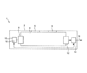
wavelengths
23 of the target analyte. Within this specification and the appended
claims, light refers to
24 electromagnetic radiation irrespective of wavelength and includes, for
example,
CA 2853963 2017-11-23
2
1 electromagnetic radiation in the infra-red region of the spectrum as this
is a region
2 within which many analyte gases have strong absorption lines.
3
4 Light emitting diodes (LEDs) are inexpensive and relatively energy
efficient devices
and so they are commonly employed as sources of light for optical absorption
gas
6 sensors, particularly devices which are intended to be small and low
cost. For many
7 applications, an LED with a peak emission wavelength in the infra-red
region of the
8 spectrum is suitable.
9
Typically, the current supplied to an LED in an optical absorption gas sensor
is
11 pulsed and, indeed, one of the advantages of LEDs is that they can be
readily pulsed.
12 There are several reasons why pulsed light sources are employed.
Firstly, pulsing the
13 source of light provides a signal at the detector which is similarly
pulsed, and so
14 which can be readily separated from noise and any background signal by
known
signal processing techniques, such as synchronous demodulation. Secondly, a
16 pulsed source of light consumes less energy than a source which emits
light
17 continuously at the same peak power consumption. Thirdly, it is known to
shape the
18 pulses, to facilitate the measurement process. Furthermore, LEDs have
maximum
19 operating currents above which the LED would be damaged by the resulting
heat
were the LED operated continuously and pulsing allows, higher maximum
operating
21 currents and therefore higher peak outputs of light than would otherwise
be the case.
22
23 One complication is that the output from an LED is sensitive to
temperature (amongst
24 other factors). As the measured gas concentration is determined from the
attenuation
of light, small effects on LED output can have a substantial effect on the
measured
26 gas concentration. The temperature of the diode junction will vary not
only with
27 ambient temperature, but also with the pulse pattern, and within
individual LED
28 pulses. This presents a technical problem, as it is necessary to control
or
29 compensate in some way for this variation with temperature. Many
photosensors are
also sensitive to temperature, amongst other factors.
31
32 In order to obtain a high signal to noise ratio, it is generally
preferable that the pulses
33 of light be relatively short but of relatively high intensity. Due to
the potential for
34 damage by excessive heat there is a trade off between maximum current
and
therefore maximum peak emitted light intensity and the duration of pulses.
However,
36 known circuits to drive LEDs to provide short pulses of light, with a
high signal-to-
CA 2853963 2017-11-23
3
1 noise ratio and clear pulse shaping, require complex control electronics
and consume
2 a substantial amount of power.
3
4 Accordingly, the invention aims to provide an alternative optical
absorption gas
sensor which employs relatively short pulses of light generated by an LED, and
6 thereby obtains accurate sensor output despite variations in LED
temperature while
7 minimising power consumption.
8
9 Summary of the invention
11 According to a first aspect of the present invention there is provided a
method of
12 operating an optical absorption gas sensor for detecting an analyte gas,
the sensor
13 comprising a gas sample receiving chamber, at least one light emitting
diode (LED)
14 and a photosensor (e.g. a photodiode) having an output signal (e.g. a
current)
sensitive to the amount of light received by the photosensor, the method
comprising
16 generating a plurality of pulses of light by passing a plurality of
pulses of current
17 through the at least one LED, and measuring the current through the at
least one
18 LED a plurality of times during each said pulse, and generating a
compensated signal
19 indicative of the concentration of an analyte gas in the gas sample
receiving chamber
taking into account both the photosensor output signal and the plurality of
21 measurements of the current through the at least one LED.
22
23 One skilled in the art will appreciate that the current through the at
least one LED can
24 be measured by directly measuring the current or, for example, by
measuring a
potential difference related to the current, for example, bypassing the
current through
26 a resistor and measuring the potential difference across the resistor.
27
28 The current through an LED is closely linked to the output of light by
the LED and so,
29 by measuring the current through the at least one LED a plurality of
times during each
pulse, features of the shape of the light pulse (variation in intensity with
time) can be
31 determined. Thus, rather than focussing only on controlling the shape of
the light
32 pulse, the invention involves measuring the shape of the light pulse, or
related
33 properties, during pulses and taking the measurements into account when
34 determining the compensated signal. This avoids the requirement for
complex
electronics to precisely control the shape of each pulse, and therefore the
cost and
36 power consumption associated with complex pulse shaping circuits.
37
CA 2853963 2017-11-23
4
1 The output of light is typically a function of the current through an
LED. Typically this
2 is a linear function up to a threshold and non-linear thereafter, or non-
linear across
3 the majority or substantially all of the useful current range,
4
In order to increase the maximum light output which can be obtained with a
broadly
6 linear relationship to current, a plurality of LEDs may be employed. They
may for
7 example be connected in series or parallel. In this case, typically the
current through
8 each may be measured. The current through each LED of a plurality of LEDs
may be
9 measured independently and than each current measurement taken into
account (for
example, summed), or the current through a plurality of LEDs connected in
series
11 and/or parallel may be measured (e.g. the current into or out of a
circuit comprising a
12 plurality of LEDs connected in series and/or parallel). However, the
method may
13 comprise measuring a current through the at least one LED and
calculating a value
14 linked to light output through the at least one LED using a non-linear
function, or a
lookup table. This latter approach is especially helpful where the at least
one LED
16 may be pulsed to a current which is not a linear function of light
output.
17
18 Preferably, the photosensor output signal (e.g. the current through a
photodiode) is
19 also measured a plurality of times during each said pulse. The plurality
of
measurements of the photosensor output signal may also be taken into account
when
21 generating the compensated signal.
22
23 Thus, by what is effectively sampling the current through the at least
one LED a
24 plurality of times during each pulse, information concerning the shape
of each pulse
(profile of light intensity versus time) can be obtained. This may, for
example, enable
26 a better estimate of the total light emitted by the at least one LED
during a pulse than
27 would be obtained by measuring current at a single instant, or by
measuring e.g.
28 peak current. Thus, the method may comprise estimating the total light
output during
29 a pulse from the measurements of current through the at least one LED a
plurality of
times during the pulse.
31
32 The current through the at least one LED and the photosensor output
signal may be
33 measured alternately (or simultaneously) during the plurality of pulses.
34
The current through the at least one LED may be measured using an analogue to
36 digital converter (ADC). The ADC may measure the potential difference
across a
37 resistor through which the current through the at least one LED is
passed. The
CA 2853963 2017-11-23
5
1 photosensor output signal may be measured by an ADC. A single ADC may be
used
2 to measure the current through the at least one LED and the photosensor
output
3 signal, for example, alternately.
4
Preferably, the current through the at least one LED, and where applicable,
the
6 photosensor output signal, are measured at least 10 times or more
preferably at least
7 20 times during each pulse.
8
9 The method preferably also includes the step of measuring the temperature
of the at
least one LED (and optionally also the temperature of the photosensor if the
11 photosensor is sensitive to temperature, for example, if the photosensor
is a
12 photodiode). The measured temperature may be taken into account when
generating
13 the compensated signal. The amount of light generated per unit of
current will vary
14 with temperature and this enables the amount of light generated to be
more
accurately determined. A plurality of measurements of the temperature of the
at least
16 one LED may be made during each pulse. The said plurality of temperature
17 measurements may be taken into account when generating the compensated
signal.
18
19 The compensated signal may by a value indicative of (e.g. proportional
to) the light
received by the photosensor. The compensated signal may be a value indicative
of
21 (e.g. proportional to the logarithm of) the concentration of the analyte
gas in the gas
22 sample receiving chamber.
23
24 The method may comprise calculating the ratio of the measured current
through the
at least one LED to the photosensor output signal, at least once and typically
a
26 plurality of times during a pulse. For example, the
ratio of the most recent, or
27 average (e.g. mean) measured current through the at least one LED to the
most
28 recent, or average (e.g. mean) photosensor output signal (e.g. the
current from a
29 photodiode) may be calculated a plurality of times during a pulse. The
said ratio may
be used to calculated the compensated signal.
31
32 The method may comprise calculating a transfer ratio of the estimated
total light
33 output from the at least one LED during a pulse (obtained from the said
current
34 measurements) to the estimated total light received by the photodiode
during the
pulse (from the measurement of the photosensor output current), or a parameter
36 related to the said transfer ratio. The said transfer ratio, or
parameter related thereto,
37 may be used to calculate the compensated signal.
CA 2853963 2017-11-23
6
1
2 The method may comprise carrying out a frequency domain analysis of a
plurality of
3 measurement of the measured current through the at least one LED and the
4 photosensor output signal (e.g. the current from a photodiode). For
example, the
method may comprise generating the pulses with a known frequency and
calculating
6 a parameter related to the energy of the measured current through the at
least one
7 LED and/or the photosensor output signal in one or more frequency bands,
for
8 example, a frequency band including the fundamental frequency (the
frequency of the
9 pulses) and one or more frequency bands including harmonics of the
fundamental
frequency (e.g. several consecutive harmonics starting from the first
harmonics, e.g.
11 first harmonic, second harmonic and third harmonic).
12
13 The pulses of current through the at least one LED may be generated by
switching off
14 a current source to an inductor and directing (the resulting) current
from the inductor
through at least one LED (and typically one or more other components such as a
16 resistor, and typically also a switch or further diode to prevent
reverse current flow
17 through the at least one LED).
18
19 It may be that one or more properties of an LED current pulse, for
example, the
maximum current during a pulse or total charge passed through the at least one
LED
21 during a pulse, are selected depending on one or more of the
measurements of the
22 current through the at least one LED carried out during an earlier LED
current pulse.
23 The one or more measurements may, for example, be the peak current
through the at
24 least one LED during an earlier pulse, or the ratio of the current
through the at least
one LED to the photosensor output signal from one or more measurements during
an
26 earlier pulse.
27
28 The one or more properties may be selected by determining the period of
time for
29 which current is supplied by a switching device (such as a transistor or
a MOSFET) to
an inductor operatively connected to (e.g. connected in series with) the at
least one
31 LED before the supply of current to the inductor is restricted
(typically stopped) by the
32 switching device. The period of time for which current is supplied to
the inductor
33 determines the total amount of energy stored in the inductor and the
magnitude of the
34 current then supplied by the inductor to the at least one LED.
36 It may be that one or more properties of an LED current pulse is
selected depending
37 on one or more measurements of the photosensor output signal, for
example to
CA 2853963 2017-11-23
7
1 control where the photosensor output signal is relative to the dynamic
range of an
2 ADC measuring the photosensor output signal. The one or more properties
may be
3 selected by determining the period of time for which current is passed
through an
4 inductor before the current source is restricted (typically stopped) to
drive current
from the inductor through the at least one LED.
6
7 The one or more properties of an LED current pulse may be selected to
compensate
8 for a measured property, e.g. the temperature of the at least one LED or
the
9 photosensor. The one or more properties of an LED current pulse may be
selected to
regulate the magnitude of the photosensor output signal, for example, to keep
the
11 photosensor output signal, or an amplified signal derived therefrom,
within a preferred
12 region of the dynamic range of an ADC, e.g. to minimise quantisation
effects or to
13 avoid the photosensor output signal, or an amplified signal derived
therefrom, from
14 exceeding the dynamic range of an ADC.
16 In addition to the said pulses during which the current through the at
least one LED is
17 measured a plurality of times (and where applicable the photosensor
output signal is
18 measured a plurality of times), there may also be pulses during which
the current
19 through the at least one LED is not measured a plurality of times
(and/or where
applicable the photosensor output signal is measured a plurality of times).
21
22 According to a second aspect of the invention there is provided an
optical absorption
23 gas sensor comprising a gas sample receiving chamber, at least one light
emitting
24 diode (LED) and a light detector (such as a photodiode) having an output
signal (e.g.
a current) sensitive to the amount of light received by the photosensor, an
LED
26 control circuit configured to generate a plurality of pulses of light in
a measurement
27 mode of the optical absorption gas sensor by passing a plurality of
pulses of current
28 through the at least one LED, measuring device configured to measure the
current
29 through the at least one LED a plurality of times during each said
pulse, and a
compensation module configured to output a compensated signal indicative of
the
31 concentration of an analyte gas in the gas sample receiving chamber,
taking into
32 account both the light detector output signal and the plurality of
measurements of the
33 current through the at least one LED.
34
The sensor to measure the current through the at least one LED may be a
current
36 sensor. However, the sensor to measure the current through the at least
one LED
37 may be a potential difference sensor configured to measure a potential
difference
CA 2853963 2017-11-23
8
1 which depends on the current through the at least one LED, for example,
the potential
2 difference across a resistor (typically a resistor connected in series
with the at least
3 one LED) through which the current from the at least one LED is passed.
4
Preferably, the gas sensor comprises a measuring device to measure the
6 photosensor output signal (e.g. a current sensor to measure the current
through a
7 photodiode) a plurality of times during each pulse. The same measuring
device may
8 measure both the current through the at least one LED and the photosensor
output
9 signal. The or each said measuring device may be an ADC. A switch may be
provided to alternately connect the sensor to an output of the at least one
LED and an
11 output of the photosensor (typically through one or more other
components, such as
12 an amplifier).
13
14 The optical absorption gas sensor preferably also comprises one or more
temperature sensors and the compensation module takes into account the one or
16 more sensed temperatures. A temperature sensor may measure the
temperature of
17 the at least one LED. A separate temperature sensor may measure the
temperature
18 of the photosensor. Temperature may be measured by measuring a parameter
19 related to temperature, such as the forward voltage, VF, across the LED
(and/oor
photodiode where the photosensor is a photodiode).
21
22 The LED control circuit may be configured to determine one or more
properties of the
23 LED pulses controlled by the LED control circuit responsive to one or
more of the
24 measurements of the current through the at least one LED and/or one of
the more of
the measurement of the photosensor output signal carried out during an earlier
LED
26 current pulse. Typically, the one or more properties of the LED pulses
are
27 determined by controlling the period of time for which current is
supplied to the
28 inductor.
29
The LED control circuit may comprise an inductor connected in series with the
at
31 least one LED (and typically one or more other components such as a
resistor). The
32 LED control circuit may be operable to supply current to the inductor
and then to
33 restrict (e.g. stop) the supply of current to the inductor, thereby
causing current to flow
34 through the at least one LED. The LED control circuit may be configured
to select the
current supplied to the inductor and/or the period of time for which the
current is
36 supplied to the inductor responsive to one or more of the measurement of
the current
CA 2853963 2017-11-23
9
1 through the at least one LED and/or one of the more of the measurement of
the
2 photosensor output signal carried out during an earlier LED current
pulse.
3
4 The optical absorption gas sensor may comprise a frequency domain
analysis
module operable to analyse of a plurality of measurement of the measured
current
6 through the at least one LED and the photosensor output signal (e.g. the
current from
7 a photodiode). For example, the optical absorption gas sensor may be
operable to
8 generate the pulses with a known frequency and comprise a frequency
domain
9 analysis module operable to calculate a parameter related to the energy
of the
measured current through the at least one LED and/or the photosensor output
signal
11 in one or more frequency bands, for example, a frequency band including
the
12 fundamental frequency (the frequency of the pulses) and one or more
frequency
13 bands including harmonics of the fundamental frequency (e.g. several
consecutive
14 harmonics starting from the first harmonics, e.g. first harmonic, second
harmonic and
third harmonic). The frequency domain analysis module may be an electronic
16 module. The frequency domain analysis module may comprise computer
program
17 code executed by a processor.
18
19 The optical absorption gas sensor is preferably adapted to selectively
measure the
concentration of a specific analyte gas, for example, by selection of one or
more of
21 the output light spectrum of the at least one LED, the spectral range
over which the
22 photosensor is sensitive and or the presence of a filter, such as a band
pass filter,
23 within the optical path (e.g. covering the at least one LED or
photosensor). The
24 optical gas sensor may be adapted to detect an analyte such as carbon
dioxide,
carbon monoxide, methane, water vapour (to measure humidity) etc. by selecting
the
26 LED and photodiode to generate and detect light specifically at one or
more
27 wavelengths where the analyte gases absorb strongly.
28
29 The at least one light emitting diode (and photodiode where the
photosensor is a
photodiode) may each be formed from a narrow band gap III-V material indium
31 aluminium antimonide material ((lni_x)AlxSb), grown on a gallium
arsenide (GaAs)
32 substrate, the doping of which is chosen to tune the band gap to cause
the light
33 emitting diode to emit light of a narrow wavelength *range corresponding
to a
34 wavelength at which the intended analyte (e.g. gaseous carbon dioxide)
absorbs
strongly. The formation of suitable light emitting diodes and photodiodes are
36 disclosed in EP 0 864 180, EP 0 992 094, and in Haigh, M.K. et al.,
Applied Physics
CA 2853963 2017-11-23
10
1 Letters, vol. 90, 231116 (2007).
2
3
4 Optional features presented in respect of the first or second aspect of
the invention
above are optional features of either the first or second aspect of the
invention.
6
7 The invention also extends in a third aspect to an optical absorption gas
sensor
8 comprising a gas sample receiving chamber, at least one light emitting
diode (LED)
9 and a light detector having an output signal sensitive to the amount of
light received
by the photosensor, and a control circuit configured to cause the optical
absorption
11 gas sensor to operate according to the method of the first aspect of the
invention.
12 The control circuit may comprise a computer readable medium (e.g. a
memory, such
13 as a ROM or PROM) storing program code and a processor (e.g. a
microcontroller)
14 operable to execute the program code.
16 Description of the Drawings
17
18 An example embodiment of the present invention will now be illustrated
with
19 reference to the following Figures in which:
21 Figure 1 is a schematic diagram of an optical absorption gas sensor;
22
23 Figure 2 is a circuit diagram for operating an optical absorption gas
sensor;
24
Figure 3 is a schematic diagram of the principle behind the inductor driven
26 mechanism for generating light pulses; and
27
28 Figure 4 is a graph of the variation in voltage at A, inductor current
and LED current
29 with time.
31 Detailed Description of an Example Embodiment
32
33 With reference to Figure 1, an optical absorption gas sensor 1 has a
body 2 defining
34 a gas sample chamber 4, into which a gas sample can pass by diffusion
through one
or more apertures 6. A light emitting diode 8 functions as a light source, and
is driven
36 by an LED control and pulse measurement circuit 10. A photodiode 12
functions as a
37 photosensor, and has an output current dependent on the light which
falls on the
CA 2853963 2017-11-23
11
1 photodiode junction. The current from the photodiode is amplified and
processed by a
2 control and compensation circuit 14 including a microcontroller, which
implements a
3 compensation function and thereby provides a compensated signal through
an output
4 16. The control and compensation circuit also receives information
concerning the
shape of LED pulses and controls the LED control circuit.
6
7 The gas sample chamber may have any of a large number of configurations
known to
8 those skilled in the art, and typically includes a reflective inner
surface, so that light
9 from the LED may be reflected one or more times between the LED and a
photodiode. The LED and photodiode may be located adjacent to each other, or
11 further apart. The optical arrangement is selected so that the
attenuation of light
12 within a wavelength characteristic of a target analyte affects the
current from the
13 photodiode. Thus, the LED may have a defined range of output
wavelengths, the
14 photodiode may be sensitive to a defined range of output wavelengths
and/or a
wavelength band pass filter may be provided.
16
17 The LED control and pulse measurement circuit includes a temperature
sensing
18 circuit 18. The temperature sensing circuit determines the temperature
of the
19 photodiode by measuring the forward voltage, Vf, across the photodiode
respectively.
Suitable circuits for determining temperature by measuring the forward voltage
are
21 disclosed in WO 2009/019467 (Gas Sensing Solutions Limited) and an
example is
22 shown in Figure 2.
23
24 Figure 2 illustrates a circuit for controlling the gas sensor, including
both the LED
control and pulse measurement circuit, LED temperature measurement circuit and
a
26 microcontroller 20 which executes program code stored on a computer
readable
27 medium, such as a ROM, and functions as the compensation module. The
system
28 power supply, V + is typically between 2.7 and 5 V. The microcontroller
20 controls
29 the overall operation of the gas sensor, and can communicate with
external devices
through a serial data interface 16. The LED 8 is driven by a inductor flyback
converter
31 controlled through a driver circuit 22 which is in turn controlled by
the microcontroller
32 which can precisely set the on and off times for a switching device in
the form of a
33 transistor 24.
34
The transistor 24 is switchable to provide current to an inductor 26 under the
control
36 of the driver circuit. The inductor is connected in parallel with a
circuit branch
37 including the LED, a second diode 28 (which functions to prevent reverse
current flow
CA 2853963 2017-11-23
12
1 through the LED, which is potentially substantial for infra-red LEDs
which have very
2 high reverse voltage leakage currents), and a resistor 30 provided to
enable the
3 current through the LED to be measured by virtue of the resulting
potential difference
4 across the resistor 30.
6 The circuit also includes the photodiode 12 and a photodiode output
signal amplifier
7 chain having first and second photodiode signal amplifiers 32 and 34 in
series. An
8 ADC 36 receives the output from the second amplification amplifier as an
input.
9
The ADC has two further inputs. One input is the output signal from an
amplifier 38
11 configured to measure the potential difference across resistor 30. The
other input to
12 the ADC is an output from a differential amplifier 40 which amplifies
the LED forward
13 voltage, for use in measuring the temperature of the LED.
14
The reference voltage VR received as an input by amplifiers 32, 34 and 38 is
selected
16 to bias these amplifiers to a suitable working point. The value of the
reference voltage
17 is not critical, although it must be stable during any given
measurement. It may, for
18 example, be at the middle of the temperature range of the ADC. To
facilitate the
19 operation of the photodiode amplifier chain, a digital to analogue
converter 42 is also
provided, under the control of the microcontroller, to introduce a selectable
offset to
21 the second amplifier of the photodiode amplifier chain via a resistor
44, so that the
22 output from the second amplifier stage can be biased to an optimum
level.
23
24 The photodiode amplifier chain is DC coupled, so that it may be turned
on or off very
quickly either by switching its power supply or using amplifier chips having
shutdown
26 capability. The first amplifier 32 of the photodiode amplifier chain
should be a low
27 noise device, and the voltage gain of the photodiode amplifier chain
should be very
28 high as the output current from a photodiode is small.
29
Figure 3 is a schematic diagram of the principle behind the inductor driven
31 mechanism for generating light pulses and Figure 4 is a graph of the
variation in
32 voltage at A, inductor current and LED current with time. A power supply
provides a
33 voltage source, V. Si is a switch (transistor, MOSFET etc.) which is
switchable to
34 open and close a circuit extending between the power supply and inductor
Li. S2 is a
further switch (a diode in the example embodiment, but S2 may also be a
transistor,
36 MOSFET etc.). LED1 is the light emitting diode (or in some embodiments a
plurality
37 of LEDs connected in series or parallel). Before each pulse, both
switches are open.
CA 2853963 2017-11-23
13
1 Si is closed, the voltage V1 is applied to the inductor. The current
through the
2 inductor therefore increases at a constant rate (dl/dt = V/L). Si is then
opened and
3 S2 closed. The inductor then drives point A negative and current flows
through the
4 inductor, S2 and the LED until the energy stored in the inductor has been
expended.
S2 can then be opened if need be. For a fixed inductor and supply voltage, the
6 energy stored in the inductor and thus the duration of the pulse is
determined by the
7 period of time for which switch Si is open.
8
9 In operation, in the circuit of Figure 2, the microcontroller controls
the driver circuit to
execute a measurement cycle comprising a plurality of light pulses. For each
pulse
11 the transistor (functioning as switch Si) is switched on and current
begins to flow into
12 the inductor. The current increases linearly with time. After a period
of time
13 determined by the controller, the transistor is switched off. As a
result, the voltage at
14 the transistor collector is driven negative by the inductor which then
acts to maintain
the current flow through the inductor as the magnetic field in the inductor is
16 discharged. The resulting current flows through the LED and resistor 30,
causing the
17 LED to generate light and the resistor to develop a potential difference
proportional to
18 the current through the LED. This continues until the potential
difference across the
19 inductor drops below the turn on threshold for the LED. (In an
alternative
embodiment, a MOSFET switched by the potential at the junction of L1 and D1 is
21 employed as the switching device).
22
23 The number of pulses in each measurement cycle, and the duration of the
pulses, is
24 typically selected according to the performance of the ADC, the
amplifier chain and
other considerations. For example, fifty pulses of 20 us duration may be
applied to
26 the LED. The inductance of the inductor is chosen to obtain a suitable
pulse length
27 and peak current. For example, the inductor may have an inductance of
200pH and
28 the peak current may be around 300mA. However, these values would depend
very
29 much on the properties of the or each LED.
31 This circuit does not carefully control the shape of individual pulses
and the precise
32 value of the current in the LED will vary according to many factors,
including the
33 supply voltage (which will often drop by a small amount after each pulse
within a
34 measurement cycle), the inductance of the inductor, and the period of
time for which
the transistor is switched on for each pulse. The invention compensates for
this by
36 measuring the current pulse in the LED and using the resulting
measurement when
37 calculating a compensated output signal. The measurements are also used
to
CA 2853963 2017-11-23
14
1 control the period of time for which current is supplied to the inductor
during
2 subsequent pulses.
3
4 The ADC alternately measures the LED current via the LED output current
amplifier
38 and then the photodiode current via first and second photodiode amplifiers
32, 34.
6 For example, a twelve bit ADC may be employed making around 1,000,000
samples
7 per second
8
9 The CPU receives the data measured by the ADC and processes it, firstly
to separate
signal from noise and background using a synchronous demodulation procedure,
11 known to one skilled in the art, and to otherwise filter and condition
the resulting
12 signal. The microcontroller then calculates the transfer ratio between
the LED light
13 output and the light measured by the photodiode. For example, it may
estimate the
14 total light output from the LED during a pulse by calculating a function
and/or reading
a lookup table to determine a measure of light output at the time when each
LED
16 current was measured from the respective LED current, and integrating
these values
17 throughout the pulse to estimate the total light output. The light
measured by the
18 photodiode can also be calculated by integrating the photodiode current
during the
19 pulse. Both of these values can be scaled and corrected as required, and
may be
integrated over many pulses. The ratio of the two can then be used as the
output
21 signal, indicative of the concentration of analyte gas.
22
23 In some embodiments, a plurality of readings (typically at least 32) of
LED current
24 and photodiode current may be taken during each pulse and all of the
various
measurements, for each of many pulses (typically at least 8 or at least 16)
may be
26 processed simultaneously, using a frequency domain analysis algorithm,
such as a
27 Fourier transform, Fast Fourier Transform, Discrete Fourier Transform or
the Goertzel
28 algorithm. In an example embodiment, the pulses are generated at a
continuous and
29 known rate. The repetition rate of the pulses and the size of the
inductor are chosen
to obtain a desired pulse duty cycle, typically between 30 and 50%. The shape
of the
31 pulses is somewhere between a square and a triangle and so most of the
energy in
32 the pulse train is contained within the fundamental, first, second and
third harmonics
33 of the pulse frequency. The sampled values of the LED current and the
photodiode
34 current, obtained using the ADC can be transformed using a Fourier
transform. From
the resulting signal, the energy in the fundamental and the harmonics can be
36 calculated. Typically, the total number of samples is a power of 2 to
simplify
37 subsequent calculations, e.g. there may be 512, 1024 or 2048 samples.
There
CA 2853963 2017-11-23
15
1 should also be an exact number of pulses in the total sample period,
which means in
2 practice that the number of pulses will be a power of 2, typically 8, 16
or 32. From the
3 Fourier transform, the amplitude of the fundamental and the harmonics,
and therefore
4 the energy of these frequency bands, can be readily calculated by
standard methods.
The ration of the total energy in the LED current in these frequency bands to
the
6 energy in the photodiode current in these frequency bands provides a
measurement
7 of the transfer ratio. This technique allows the signals to be both
filtered and
8 averaged in one mathematical operation. Typically, the
Fourier transform is
9 calculated by a computationally efficient method known to those skilled
in digital
signal processing, such as Fast Fourier Transform or the Goertzel algorithm
11
12 This approach is also advantageous as a difficulty with pulse by pulse
measuring is
13 that the power supply usually drops a little with each pulse. Whilst
methods exist to
14 prevent this they are costly in terms of parts and power consumption. If
each pulse is
different the transfer ratio should be calculated for each individual pulse
and this
16 requires the time at which each pulse starts and stops to be known very
accurately.
17 This can mean that the signal processing requires a greater bandwidth
than is
18 otherwise desirable and increases the overall noise. Accordingly, the
frequency
19 domain analysis provides a useful approach for cost and time efficient
data
processing.
21
22 Furthermore, the microcontroller dynamically varies the period of time
for which the
23 transistor is switched on from one current pulse to the next. The
transfer ratio varies
24 significantly with temperature and so by adjusting the period of time
for which the
transistor is on, the processor can keep the amplitude of the photodiode
signal from
26 becoming too large at low temperatures, or too small at high
temperatures, for
27 accurate readings to be obtained. This ensures that ADC quantisation
noise does not
28 adversely affect the system at high temperatures, and enables the
dynamic range of
29 the ADC to be appropriately employed.
31 Differential amplifier 40 provides a measurement of the forward voltage
of the LED.
32 This can be used to establish the temperature of the LED as the forward
voltage is a
33 function of temperature. A relationship between forward voltage and
temperature can
34 be stored in a lookup table. The controller may, for example, cause a
low current
pulse or pulses to be applied to the LED at the beginning of a measuring cycle
(each
36 cycle into the product of pulses) to measure the temperature in the LED.
The output
37 from the differential amplifier at that time is processed by the ADC.
CA 2853963 2017-11-23
16
1
2 As a result, shorter LED pulses can be employed than would be the case if
the shape
3 of each pulse had to be carefully controlled. Furthermore, the use of the
inductor
4 enables peak LED current to be determined independently of supply
voltage. Thus,
short high amplitude pulses can be employed. This in turn improves the signal
to
6 noise ratio of the measuring system as a whole (photodiode, ADC and
7 microcontroller) because, although shorter pulses require a larger
bandwidth, thermal
8 noise (which is the dominant source of noise in the amplifier chain)
increases with the
9 square root of bandwidth but the photodiode output signal increases
linearly. If, for
example, peak LED current was increased from 50mA to 200mA and the duration of
11 each pulse reduced by a factor of four, the noise would only increase by
a factor of
12 two. In practice, LEDs have series resistance which reduces the
efficiency as the
13 current increases so that gain in signal to noise ration is less than
would be
14 anticipated. Nevertheless, the net effect is an improvement in signal to
noise ratio.
16 The ability to dynamically adjust LED current and offset also reduces
ADC noise
17 effects. The invention also has the benefit that measurements may be
carried out
18 very quickly. For example, it may be possible to carry out an entire
measurement in
19 less than 10 ms, including taking a temperature measurement, measuring
LED and
photodiode current during fifty light pulses, and processing the resulting
data. The
21 procedure may therefore be repeated and averaged and still provide a
rapid result,
22 although each repetition increases the total power output.
23
24 The circuit illustrated in Figure 2 also has the advantage of being
energy-efficient in
comparison with simple circuits for driving LEDs employing a resistor in
series with
26 the LED, or an active current source. Furthermore, most such circuits
require power
27 supplies well in excess of 3 V. A suitable switching regulator can of
course convert a
28 3 V supply at a higher voltage although this would reduce efficiency.
29
The sensor is tolerant of a reasonable temperature differential between LED
and
31 photosensor, enabling the LED and photosensor to be spaced apart, for
example, at
32 opposite ends of a waveguide.
33
34 In an alternative embodiment, a plurality of LEDs are provided,
connected in series or
parallel, and the current through the plurality of LEDs is measured. This
increases
36 the range of light output over which the current is a roughly linear
function of light
CA 2853963 2017-11-23
17
1 output, or at least sufficiently sensitive to light output to enable
light output to be
2 estimated with reasonable accuracy.
3
4 In some embodiments, a resistor is placed in series with the inductor
(L1) and the
potential difference across that series resistor in order to measure the
current through
6 the inductor. This enables the micro controller to regulate the pulses
which are
7 generated to ensure that the current in the inductor does not exceed a
threshold.
8
9 Further variations and modifications may be made by one skilled in the
art within the
scope of the invention herein disclosed.
11
CA 2853963 2017-11-23