Note: Descriptions are shown in the official language in which they were submitted.
CA 02854438 2014-05-02
WO 2013/066332 PCT/US2011/059142
CONTROL SYSTEM FOR SYNCHRONOUS CAPACITOR SWITCH
BACKGROUND
[0001] The present disclosure relates generally to the field of electrical
switch control
systems. More specifically, the present disclosure relates to systems and
methods for
controlling a switch to selectively connect a power source (e.g., a three
phase, medium
voltage power source) to one or more capacitors.
[0002] Switched capacitor banks are installed on poles and at sub stations to
apply power
factor correction (e.g., by altering the load phasing) to the power grid in
response to the
application and removal of heavy industrial inductive loads such as motors.
When loads are
not in phase, additional reactive currents increase transmission losses which
results in
wasted energy and the need for additional generating capacity. In some
systems, a separate
control senses the voltage-to-current phase relationship and commands the
capacitor switch
to open and close based on the relationship. Applying capacitors may help
improve the
transfer efficiency of the electrical energy being transmitted through the
power grid.
Medium voltage applications (e.g., 5 kV ¨ 38 kV) often include capacitors that
are switched
on and off based on power factor correction needs.
[0003] If a switch closes at a time when the AC voltage across the switch is
not at a
waveform zero, disturbances may occur due to heavy inrush currents as the
capacitors are
charged. The disturbances may include, for example, voltage dips, harmonics,
resonance
peaks and/or other undesirable effects on the electrical system. Such
disturbances can cause
problems with sensitive customer equipment, such as industrial VFD (variable
frequency
drive) motor controllers. Due to the mechanical and electrical complexity, the
majority of
medium voltage capacitor switches close randomly with respect to voltage. Some
systems
are configured with a resistor inserted in series with the switch to charge
the capacitor to
voltage, reducing the inrush current. Such systems may be acceptable for some
applications, but may not perform in an acceptable fashion for more sensitive
applications.
[0004] Controllers that are configured to close when the voltage across the
capacitor
switch is nearly zero volts are typically complex, expensive, and difficult to
commission/install because they must handle a complex mixture of mechanical
and
electrical variations. Complex algorithms may be used to estimate the voltage
across each
-1-
CA 02854438 2014-05-02
WO 2013/066332 PCT/US2011/059142
switch, and such algorithms may require the installer to provide detailed
information about
the installation, such as the phase rotation (e.g., A-B-C phasing or A-C-B
phasing),
Wye/Delta capacitor connections and capacitor grounding (e.g., grounded or
ungrounded).
Some controllers blindly time their operations based on a single phase voltage
sensor and
calibration information regarding the electrical system to which the system is
connected.
For example, a voltage sensing transformer may reference only phase A of a
three phase
system. If the capacitor bank is connected in a grounded Wye configuration, it
is expected
that the electrical timing between zero volts of each phase is separated by
120 electrical
degrees. The phase rotation must be known to configure such a controller.
[0005] Additionally, conventional zero-closing switches are configured to
measure
voltage on a single side of the switch (e.g., the power source side). When a
Medium
Voltage AC switch operating a capacitor opens, the current is cleared at a
zero crossing.
Since the current and voltage signals are out of phase 90 degrees due to the
capacitor, a near
peak trapped DC charge is left on the capacitor after the switch is opened.
Capacitors have
an internal resistor that is configured to slowly dissipate this energy until
the voltage across
the capacitor is brought to zero volts. In order to ensure that the capacitor
has fully
discharged (e.g,. such that the voltage on the capacitor side of the switch is
zero) and that
closing the switch will not induce abnormally large inrush current (e.g., more
than 6 times
load capacitive load current), conventional zero-closing switches may be
configured to wait
a predetermined amount of time (e.g., five minutes) after the switch was last
opened before
closing the switch again. Closing the switch prior to the predetermined amount
of time may
produce an abnormally large inrush current (e.g., up to 80 times load current)
as the source
voltage meets a large trapped charge voltage on the capacitor. Specialized
interlocking
control equipment, training, and/or signage is often used to prevent closing
of the switch
prior to the passage of the predetermined amount of time.
[0006] There is a need for an improved control system for controlling the
operation of
switches used to selectively connect power sources to switched capacitors.
There is also a
need for a control system that is highly repeatable under a variety of
environmental
conditions. Further, there is a need for a control system that can be
connected to a variety
of different power system and/or capacitor configurations without the need for
a substantial
amount of specialized calibration to the individual types of configurations.
Further still,
there is a need for a control system that provides greater knowledge and
awareness of the
voltage conditions on both sides of the switch. There is also a need for a
control system that
-2-
CA 02854438 2014-05-02
WO 2013/066332 PCT/US2011/059142
does not require the switch to wait a predetermined amount of time after
opening before the
switch may close again.
SUMMARY
[0007] One exemplary embodiment of the disclosure relates to a method of
controlling the
connection of a multiple phase power source to a plurality of capacitors. Each
phase of the
multiple phase power source is electrically connectable to at least one of the
plurality of
capacitors through a switching device. The method comprises, for each phase of
the
multiple phase power source, determining a first voltage of a power signal for
the respective
phase of the power source using a first voltage divider that is electrically
connected to a first
terminal of the switching device for the phase. The method further comprises,
for each
phase, determining a second voltage across a capacitor that is electrically
connected to a
second terminal of the switching device for the phase. The second voltage is
determined
using a second voltage divider that is electrically connected to the second
terminal of the
switching device for the phase. The method further comprises, for each phase,
generating a
close signal configured to cause the switching device for the phase to close
and electrically
connect the respective phase of the power source to the capacitor when the
difference
between the first voltage and the second voltage is approximately zero.
[0008] Another exemplary embodiment of the disclosure relates to a control
system for
controlling the connection of a multiple phase power source to a plurality of
capacitors.
Each phase of the multiple phase power source is electrically connectable to
at least one of
the plurality of capacitors through a switching device. The control system
comprises a
control circuit. The control circuit is configured to, for each phase of the
multiple phase
power source, determine a first voltage of a power signal for the respective
phase of the
power source using a first voltage divider that is electrically connected to a
first terminal of
the switching device for the phase. The control circuit is further configured
to, for each
phase, determine a second voltage across a capacitor that is electrically
connected to a
second terminal of the switching device for the phase. The second voltage is
determined
using a second voltage divider that is electrically connected to the second
terminal of the
switching device for the phase. The control circuit is further configured to,
for each phase,
generate a close signal configured to cause the switching device for the phase
to close and
electrically connect the respective phase of the power source to the capacitor
when the
difference between the first voltage and the second voltage is approximately
zero.
-3-
10008A1 In a broad aspect, the invention pertains to a method of
controlling the
connection of a multiple phase power source to a plurality of capacitors,
wherein each phase
of the multiple phase power source is electrically connectable to at least one
of the plurality of
capacitors through a switching device. For each phase of the multiple phase
power source,
the method comprises determining a first voltage of a power signal for the
respective phase of
the power source using a first voltage divider that is electrically connected
to a first terminal
of the switching device for the phase. The first voltage divider has a first
high voltage
resistor and a first low voltage resistor, wherein the first voltage is equal
to a voltage across
the first low voltage resistor. A second voltage is determined across a
capacitor that is
electrically connected to a second terminal of the switching device for the
phase, the second
voltage being determined using a second voltage divider that is electrically
connected to the
second terminal of the switching device for the phase. The second voltage
divider has a
second high voltage resistor and a second low voltage resistor, the second
voltage being equal
to a voltage across the second low voltage resistor. A close signal is
generated and is
configured to cause the switching device for the phase to close and
electrically connect the
respective phase of the power source to the capacitor when the difference
between the first
voltage and the second voltage is approximately zero.
10008B1 In a further aspect, the invention provides a control system
for controlling the
connection of a multiple phase power source to a plurality of capacitors. Each
phase of the
multiple phase power source is electrically connectable to at least one of the
plurality of
capacitors through a switching device. The control system comprises a control
circuit
configured to, for each phase of the multiple phase power source, determine a
first voltage of
a power signal for the respective phase of the power source using a first
voltage divider that
is electrically connected to a first terminal of the switching device for the
phase. The first
voltage divider has a first high voltage resistor and a first low voltage
resistor, the first
voltage being equal to a voltage across the first low voltage resistor. A
second voltage is
determined across a capacitor that is electrically connected to a second
terminal of the
switching device for the phase. The second voltage is determined using a
second voltage
divider that is electrically connected to the second terminal of the switching
device for the
phase, the second voltage divider having a second high voltage resistor and a
second low
voltage resistor, the second voltage being equal to a voltage across the
second low voltage
resistor. A close signal is generated and is configured to cause the switching
device for the
phase to close and electrically connect the respective phase of the power
source to the
capacitor when the difference between the first voltage and the second voltage
is
approximately zero.
- 3a -
CA 2854438 2017-12-13
CA 02854438 2014-05-02
WO 2013/066332 PCT/US2011/059142
BRIEF DESCRIPTION OF THE DRAWINGS
[0009] FIG. 1 is a block diagram of a control system that may be used to
control the
operation of switching devices for selectively connecting a three phase
voltage source to
switched capacitors according to an exemplary embodiment.
[0010] FIG. 2 is a single-phase block diagram of the control system shown in
FIG. 1
according to an exemplary embodiment.
[0011] FIG. 3 is a flow diagram for a process of controlling the operation of
a switching
device for connecting a voltage source to a switched capacitor according to an
exemplary
embodiment.
[0012] FIG. 4 is a single-phase schematic electrical diagram of a control
system for
controlling the operation of a switching device for connecting a voltage
source to a switched
capacitor according to an exemplary embodiment.
[0013] FIG. 5 is a perspective view of a control system that may be used to
control the
operation of switching devices for selectively connecting a three phase
voltage source to
switched capacitors according to an exemplary embodiment.
[0014] FIG. 6 is a back planar view of the control system of FIG. 5 according
to an
exemplary embodiment.
[0015] FIG. 7 is a perspective view of a lateral cross-section of the control
system shown
in FIG. 5 according to an exemplary embodiment.
[0016] FIG. 8 is a front planar view of a lateral cross-section of the control
system shown
in FIG. 5 according to an exemplary embodiment.
100171 FIG. 9 is a front planar view of a switching device that may be used to
connect
and/or disconnect a voltage source to a switched capacitor according to an
exemplary
embodiment.
[0018] FIG. 10 is a rear planar view of the switching device of FIG. 9
according to an
exemplary embodiment.
[0019] FIG. 11 is a schematic illustration of an operating rod that may be
used in
connecting and/or disconnecting a voltage source to a switched capacitor
according to an
exemplary embodiment.
DETAILED DESCRIPTION
[0020] Before turning to the Figures, it should be noted that references to
"front," "back,"
"rear," "upward," "downward," "inner," "outer," "right," "left," and/or other
directional
-4-
CA 02854438 2014-05-02
WO 2013/066332 PCT/US2011/059142
terms in this description are merely used to identify the various elements as
they are
oriented in the Figures. These terms are not meant to limit the element which
they describe,
as the various elements may be oriented differently in various applications.
[0021] Referring generally to the Figures, systems and methods for controlling
the
connection between a power source, such as a multiple-phase (e.g., three
phase) power
source, and one or more capacitors are provided according to various exemplary
embodiments. A switch system may be comprised of a separate switching device
or
contactor for each phase of a multiple-phase system (e.g., three contactors
for three phases).
In various embodiments, for each phase, separate voltage dividers may be
provided on each
side of the switching device (e.g., one on the capacitor or load side, another
on the power
source or grid side). The voltage dividers may be used to determine the
voltage on each
side of the switching device for the phase. A control circuit may compare the
determined
voltages to decide if and when the voltage across the switch (e.g., the
difference between
the voltages on the opposite sides of the switch) is approaching approximately
zero. The
control circuit may then generate a signal (e.g., a close signal) that may be
transmitted to the
switching device to cause the switching device to close and form an electrical
connection
between the power source and the one or more capacitors at about the time when
the
difference in the voltages approaches approximately zero volts.
100221 In various exemplary embodiments (e.g., systems and/or methods),
various
features may be utilized to control the connection between a power source and
switched
capacitors. For example, a close signal may be generated before the capacitor
is fully
discharged. The close signal may be generated a predetermined time prior to
when the
difference between the first voltage and the second voltage is expected to
approach
approximately zero. The predetermined time may be based on a time delay
between a time
when the switching device receives the close signal and a time when the
switching device
comes to rest in a closed position. The time delay may be determined by
applying a voltage
across the first and second terminals of the switching device at a first time,
closing the
switching device, and determining a second time at which the voltage
approaches
approximately zero, wherein the time delay comprises the difference between
the first time
and the second time.
[0023] A power supply may be provided that is configured to provide an
approximately
constant current to power the switching device.
[0024] The switching device may comprise a rod configured to be moved between
a first
position in which the switching device is in an open position and a second
position in which
-5-
CA 02854438 2014-05-02
WO 2013/066332 PCT/US2011/059142
the switching device is in a closed position. At least a portion of the first
voltage divider or
second voltage divider may be positioned within the rod. The voltage divider
positioned
within the rod may include one or more high voltage thick film resistors. The
resistor(s)
may be encapsulated within a urethane material.
[0025] Referring now to FIG. 1, a block diagram of a control system 100 that
may be used
to control the operation of switching devices for selectively connecting a
three phase
voltage source to switched capacitors is shown according to an exemplary
embodiment.
System 100 may be used to control the time at which three switching devices
160, 165, and
170 (e.g., one for each of the three phases of the power source) of a three
phase switching
system close and form an electrical connection between the power source and
the
capacitors. While system 100 is illustrated as being applied to a three phase
system, the
features of system 100 described herein may be applied to any single-phase or
multiple-
phase power system.
[0026] System 100 includes a control circuit 105 configured to receive input
signals from
voltage dividers and generate control signals for controlling the operation of
switching
devices based on the input signals. In some embodiments, control circuit 105
includes a
processor 110 and a memory 115. Processor 110 may be any type of general or
special
purpose processing circuit or device. Memory 115 may be any type of machine-
readable
medium, such as flash memory, RAM, ROM, etc.
[0027] Memory 115 may include one or more modules configured to perform
various
functions of control circuit 105. For example, memory 115 may include a
voltage
comparator module 120 configured to compare voltages received from voltage
dividers and
determine when the difference between the voltages is approaching
approximately zero.
Memory 115 may additionally or alternatively include a switch control module
configured
to generate signals (e.g., close and/or open signals) configured to instruct
the switching
devices to open or close. In some embodiments, the modules may be implemented
using
machine-executable instructions stored in memory 115 and executable by
processor 105. In
some embodiments, some or all of the functions of control circuit 105 such as
comparing
input voltages and/or sending control signals to switching devices, may be
implemented
using circuitry other than a processor and/or memory.
[0028] Control circuit 105 is configured to receive voltage signals from at
least two
voltage dividers for each phase of the multiple-phase power system. As
illustrated, control
circuit receives a voltage input signal from a first voltage divider 130 for
phase A (e.g., a
power source-side voltage divider for phase A), a second voltage divider 135
for phase A
-6-
CA 02854438 2014-05-02
WO 2013/066332 PCT/US2011/059142
(e.g., a capacitor or load-side voltage divider for phase A), a first voltage
divider 140 for
phase B (e.g., a power source-side voltage divider for phase B), a second
voltage divider
145 for phase B (e.g., a capacitor or load-side voltage divider for phase B),
a first voltage
divider 150 for phase C (e.g., a power source-side voltage divider for phase
C), and a
second voltage divider 155 for phase C (e.g., a capacitor or load-side voltage
divider for
phase C). In some embodiments, a low voltage terminal or lead of each of the
voltage
dividers and/or of control circuit 105 may be connected to the same low
voltage reference or
ground terminal.
[0029] Control circuit 105 is configured to generate signals for transmission
to phase A
switching device 160, phase B switching device 165, and phase C switching
device 170
based on the voltage inputs from the respective phase voltage dividers. For
example,
control circuit 105 is configured to generate control signals for phase A
switching device
160 based on the voltage inputs from voltage dividers 130 and 135, to generate
control
signals for phase B switching device 165 based on the voltage inputs from
voltage dividers
140 and 145, and to generate control signals for phase C switching device 170
based on
voltage inputs from voltage dividers 150 and 155. In some embodiments, a
single control
circuit may be used to control the operation of switching devices for all
phases. In other
embodiments, multiple control circuits (e.g., a control circuit for each
phase) may be
utilized to control the operation of the switching devices.
[0030] Referring now to FIG. 2, a block diagram of single-phase system 200 of
control
system 100 that is illustrated in FIG. 1 is shown according to an exemplary
embodiment.
Single-phase system 200 illustrates the operation of control circuit 105 in
controlling the
connection of a single phase A to one or more capacitors using phase A
switching device
160. Control circuit 105 is configured to measure the voltage on the source or
grid side of
switching device 160 using voltage divider 130. The voltage measured using
voltage
divider 130 may represent the voltage (e.g., alternating current, or AC,
voltage) of a single-
phase source power signal being transmitted on the phase A pole of the
multiple-phase
power system. Control circuit 105 is configured to measure the voltage on the
load or
capacitor side of switching device 160 using voltage divider 135. The voltage
measured
using voltage divider 135 may represent the voltage (e.g., direct current, or
DC, voltage)
across the capacitor (e.g., due to the energy stored in the capacitor).
[0031] Control circuit 105 may be configured to monitor the difference between
the
voltages on the source and load sides of switching device 160. If the
difference between the
voltages does not approach approximately zero volts, control circuit 105 may
be configured
-7-
CA 02854438 2014-05-02
WO 2013/066332 PCT/US2011/059142
to not generate a close signal and switching device 160 may remain in an open
configuration. When the difference between the voltages on the source and load
sides
approaches approximately zero (e.g., if the voltages are approximately the
same), control
circuit 105 may be configured to generate a close signal and transmit the
signal to switching
device 160, causing switching device 160 to close and form an electrical
connection
between the power source and the capacitor(s). In some embodiments, control
circuit 105
may be configured to maintain closure of the switching devices within +/- 10
degrees of
zero-crossing. Because switching device 160 closes when the voltage difference
between
the source and load sides is approximately zero volts, no substantial in-rush
current should
flow in the resulting circuit and undesirable effects of connecting to the
capacitor(s) are be
reduced or avoided.
[0032] Some existing designs utilize voltage transformers to provide a
reference signal for
proper electrical contact closure sequencing. Because voltage transformers can
be
configured in either phase to phase or phase to ground wiring configurations,
such
variations must be accounted for in the control scheme and configured upon
setup.
[0033] By utilizing voltage dividers on both sides of switching device 160,
the
instantaneous DC component of the voltage is available. Control circuit 105
can use the
voltage divider inputs to determine the actual voltage differential across
switching device
160. Accordingly, control circuit 105 can independently determine the voltage
zero for
each phase and does not need to have knowledge of the phase rotation (e.g., A-
B-C or A-C-
B phasing) of the power system. Further, because the voltage dividers are used
to determine
the actual voltage on each side of switching device 160 independently (e.g.,
as opposed to
inferring the voltage on one side based on a measurement of the other side and
knowledge
of the configuration of the power system), control circuit 105 need not be
calibrated with
the specific configuration of the power system (e.g., Delta/Wye,
grounded/ungrounded, etc.)
in order to determine the appropriate zero or near-zero point at which
switching device 160
should close. Further, no substantial in-rush current should occur as long as
the voltage
differential between the two sides of switching device 160 is approximately
zero, even if the
capacitor is still holding a charge. Accordingly, control circuit 105 does not
need to wait a
predetermined amount of time (e.g., five minutes) after the capacitor has last
opened before
switching device 160 can be closed again.
[0034] In some embodiments, control circuit 105 may also be used to generate
control
signals to cause switching device 160 to open. Current transducers may be used
to
determine an appropriate zero-current opening time. In some embodiments,
control circuit
-8-
CA 02854438 2014-05-02
WO 2013/066332 PCT/US2011/059142
105 may be configured to generate an open signal without using current
transducers by
monitoring the load-side voltage signal. Because the capacitors cause the
current signal to
lead the voltage signal on the load side by 90 degrees, the proper zero-
current opening time
may be calculated by control circuit 105.
100351 Referring now to FIG. 3, a flow diagram for a process 300 of
controlling the
operation of a switching device for connecting a voltage source to a switched
capacitor
according to an exemplary embodiment. In various embodiments, process 300 may
be
implemented using control circuit 105 in a single phase as illustrated in FIG.
2 and/or
applied to multiple phases as illustrated in FIG. 1. As illustrated in FIG. 3,
process 300
includes operations that may be used to control the connection of a single
phase of a power
system to one or more capacitors. In some embodiments, a control circuit may
be
configured to utilize process 300 to control each phase of a multiple-phase
power system
independently (e.g., such that process 300 is repeated for each phase).
[0036] The control circuit may be configured to determine a source-side
voltage
associated with a power signal for a phase of a connected power system using a
voltage
signal received from a first voltage divider (operation 305). The first
voltage divider may
be electrically connected to the source side of a switching device for the
phase. The control
circuit may be configured to determine a load-side voltage, or voltage across
a capacitor
connected to a second side of the switching device, using another voltage
signal received
from a second voltage divider for the phase (operation 310). The second
voltage divider
may be electrically connected to the load, or capacitor, side of the switching
device for the
phase.
[0037] The control circuit may be configured to determine a voltage
differential across the
switching device for the phase using the voltage signals from the first and
second voltage
dividers. The control circuit may be configured to monitor the voltage
differential to
determine if the voltage differential is approaching approximately zero volts
(e.g., such that
the source-side voltage and the load-side voltage are approximately the same)
(operation
315). If the voltage differential is not approximately zero volts, the control
circuit may
continue to monitor the voltage signals received from the voltage dividers and
may not
generate a signal to cause the switching device for the phase to open. When
the voltage
differential is determined to be approximately zero, such as when the
capacitor is fully
discharged and the source side voltage is zero, or when the same non-zero
voltage is present
in the source power signal for the phase and across the capacitor, the control
circuit may be
configured to generate a close signal and transmit the close signal to the
switching device
-9-
CA 02854438 2014-05-02
WO 2013/066332 PCT/US2011/059142
(operation 320). The switching device may be configured to close and
electrically connect
the respective phase or pole of the power system to the capacitor(s) when the
voltage
differential across the switching device is approximately zero volts in
response to receiving
the close signal from the control circuit.
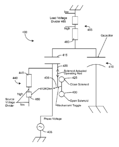
[0038] Referring now to FIG. 4, a single-phase schematic electrical diagram
400 of a
control system for controlling the operation of a switching device for
connecting a voltage
source to a switched capacitor is shown according to an exemplary embodiment.
Electrical
diagram 400 may represent a high-level electrical implementation of control
system 200
and/or a single phase of control system 100 in some exemplary embodiments. In
some
embodiments, the circuit illustrated in electrical diagram 400 may be applied
to control the
connection of a voltage source to a switched capacitor using one or more
operations of
process 300.
[0039] As illustrated in electrical diagram 400, the control system includes a
power source
405 (e.g., an AC voltage source, such as a high voltage power source from a
power grid)
and a capacitor 410 (e.g., one or more capacitors, such as in a capacitor
bank) that are
selectively connectable through the use of a switching device. In some
embodiments, the
voltage of power source 405 may be as high as 22 kV or higher. The switching
device
includes a pair of contactors 415 that may be moved in contact with one
another (e.g., in a
closed position of the switching device) and separated from one another (e.g.,
in an open
position of the switching device) to enable and disable, respectively, an
electrical
connection between power source 405 and capacitor 410.
[0040] In some embodiments, one or both of contactors 415 may be operatively
moved in
and out of contact with the other contactor 415 through the use of a solenoid
assembly or
other type of actuator. In electrical diagram 400, two solenoid devices are
used in
conjunction with an operating rod 420 to move the source-side contactor into
and out of
contact with the load-side (e.g., capacitor-side) contactor. A close solenoid
425 is
configured to push operating rod 420 up, moving the source-side contactor into
contact with
the capacitor-side contactor. An open solenoid 430 is configured to pull
operating rod 420
down, moving the source-side contactor out of contact with the capacitor-side
contactor. A
toggle switch 435 or other mechanism may be used to control the operation of
the solenoid
devices. In some embodiments, one solenoid device may be used to perform both
the
opening and closing functions of the switching device. In some embodiments, a
different
type of actuating device may be used to open and close the connection between
power
source 405 and capacitor 410.
-10-
CA 02854438 2014-05-02
WO 2013/066332 PCT/US2011/059142
[0041] Electrical diagram 400 also includes two separate voltage dividers, one
electrically
connected to the source side of contactors 415 and one electrically connected
to the
capacitor side of contactors 415. Source-side voltage divider 440 includes two
or more
resistors and may be used by a control circuit to determine the voltage (e.g.,
AC voltage) of
power source 405 at any given point in time. Voltage divider 440 may be
connected in a
parallel configuration with power source 405, such that a high voltage side of
voltage
divider 440 may be electrically connected with a high voltage side of power
source 405, and
a low voltage side of voltage divider 440 may be connected to a low voltage
terminal (e.g.,
ground terminal, very high impedance element, etc.). In such a configuration,
the voltage
across voltage divider 440 is the same as the voltage of power source 405.
[0042] Voltage divider 440 may include at least a first resistor 445 and a
second resistor
450. Resistor 445 may be a high voltage resistor configured to withstand a
high voltage
drop across the resistor without damaging the resistor, such as a high voltage
thick film
resistor (e.g., 1 Gfl, 10 Gil, 10 Mil, etc.). Resistor 450 may be a lower
voltage resistor
(e.g., as compared to resistor 445) and may be configured such that the
voltage drop across
resistor 450 is substantially lower than the voltage drop across resistor 445
during operation.
A control circuit may be configured to measure the voltage across resistor 450
(e.g., by
using an electrical connection, such as a wire lead, to a high voltage side of
resistor 450
and/or a low voltage side of resistor 450). The voltage across resistor 450
can be used to
determine the voltage across the entire voltage divider 440 because the
voltage across
resistor 450 is directly related to the total voltage based on the relative
resistance values of
resistors 445 and 450. The total voltage across voltage divider 440 (and,
accordingly, the
voltage of power source 405) can be determined according to the following
expression,
where VVD440 represents the total voltage across voltage divider 440, R445 and
R450 represent
the resistance values of resistors 445 and 450, respectively (e.g., in ohms),
and VR450
represents the voltage measured across the smaller resistor 450:
[0043] Vv1J440 = ((R445 R450)/R445) X VR450
[0044] By measuring across the smaller resistor 450, the voltage may be
reduced to a level
that is safe for the electronics of the control circuit used to measure the
voltage value. In
some embodiments, both resistors 445 and 450 may be included as part of a
voltage divider
assembly. In some embodiments, resistor 445 may be included in a separate
assembly from
resistor 450. For example, resistor 445 may be included in an assembly
configured to
encapsulate a high voltage resistor, and resistor 450 may be mounted or
embedded on a
circuit board, such as a circuit board of the control circuit.
-11-
CA 02854438 2014-05-02
WO 2013/066332
PCT/US2011/059142
[0045] A second voltage divider 455 is electrically connected to the capacitor
side of the
contactors 415. Capacitor-side voltage divider 455 includes two or more
resistors and may
be used by the control circuit to determine the voltage (e.g., DC voltage)
across capacitor
410. Voltage divider 455 may be connected in a parallel configuration with
capacitor 410,
such that a high voltage side of voltage divider 455 is electrically connected
to a high
voltage side of capacitor 410 and a low voltage side of voltage divider 455 is
electrically
connected to a low voltage terminal.
[0046] Capacitor-side voltage divider 455 may include at least a first
resistor 460 and a
second resistor 465. Resistor 460 may be a high voltage resistor and resistor
465 may be a
lower-voltage resistor (e.g., resistor 460 might have a higher resistance
value than resistor
465). The control circuit may be configured to measure the voltage across the
smaller
resistor 465 and use that voltage value to determine the voltage across the
entire voltage
divider 455 and, accordingly, the voltage across capacitor 410. The voltage
across voltage
divider 455 may be determined in the same manner described above with respect
to voltage
divider 445. In various embodiments, resistors 460 and/or 465 may have the
same or
different resistance values as resistors 445 and 450, respectively.
[0047] Referring now to FIG. 5, a perspective view of a control system 500
that may be
used to control the operation of switching devices for selectively connecting
a three phase
voltage source to switched capacitors is shown according to an exemplary
embodiment.
System 500 includes three single-phase switching systems 505, one for
connection to each
phase or pole of the power source. Each single-phase system 505 includes a
housing 510
configured to enclose a switching device used to connect and disconnect the
phase to a
capacitor. The phase of the power source may be connected at a terminal 515,
and the
capacitor(s) may be connected at another terminal 520. Each single-phase
system 505
includes a source-side voltage divider (not visible in FIG. 5) and a capacitor-
side voltage
divider 525 (e.g., an external voltage divider electrically connected to a
capacitor or load
side of the switching device for the phase) that may be used to determine the
voltages at
each side of the switching device for the phase. The switching devices and
voltage dividers
for all three phases may be provided in one integrated control system such
that control
system 500 is a "hook up and go" type system that is as easy to install as non-
zero-close
systems. In some embodiments, a system similar to control system 500 may be
used in the
implementation of various systems and methods described herein (e.g., systems
100 and/or
200, process 300, the electrical system illustrated in diagram 400, etc.) and
control system
500 may incorporate various features described with respect to those systems
and methods.
-12-
CA 02854438 2014-05-02
WO 2013/066332 PCT/US2011/059142
[0048] Referring now to FIG. 6, a back planar view of control system 500 of
FIG. 5 is
shown according to an exemplary embodiment. In this view, a power supply input
interface
605 and a control input interface 610 of system 500 are shown. Control input
interface 610
may be used to receive control input signals to control the operation of the
switching
devices for each phase and/or to calibrate system 500. For example, a
technician may
connect a computing device to one or more terminals of control input interface
to provide
calibration values to system 500, test system 500, manually open and/or close
one or more
of the switching devices, etc. In some embodiments, control input interface
610 may
provide a separate control input for each phase of the three phase power
source.
[0049] In some embodiments, control system 500 may be calibrated once (e.g.,
at a
factory, during production) and may not need subsequent calibration to operate
accurately
once installed on a power grid node. Calibration may include defining a time
delay from
when the control circuit provides a signal to close the switching device until
the time at
which the contacts of the switching device are actually closed and in contact.
Initial
calibration may be accomplished by applying a voltage across the capacitor
switch source
and load main terminals. The control can be put in a calibration mode and use
feedback
regarding the voltage differential across the terminals to calculate the time
delay (e.g., the
time it takes from the transmission of the signal before the voltage
differential approaches
approximately zero). The time delay may be stored in the control circuit as a
constant
value. In some embodiments, a similar process may be used to provide a
feedback to the
control circuit during operation (e.g., for error detection and/or to make
incremental
adjustments to the time delay value due to changes in the switch response
time).
[0050] Power supply input interface 605 may be used to receive operating power
(e.g.,
120 VAC, 50 Hz or 60 Hz, 1000 VA, etc.) for the switching devices (e.g.,
solenoid devices)
from a power supply. Some controllers use energy stored in capacitors to
operate the
solenoid or actuator in the switch. Since capacitor energy varies with
temperature, as does
solenoid winding resistance, many variables may be used to account for proper
temperature
compensation.
[0051] One way to provide increased repeatability and consistency is to use a
constant
current power supply to power the switching devices. Solenoids devices, for
example, have
a set number of turns in their coils, and the output of the solenoid devices
is based on the
product of the number of turns and the current applied. Using a power supply
that provides
a constant current power signal to power the solenoid devices reduces the
number and
complexity of variables associated with changes in capacitance and/or solenoid
winding
-13-
CA 02854438 2014-05-02
WO 2013/066332 PCT/US2011/059142
resistance due to temperature. In some embodiments, a pulse width modulated
(PWM)
current-related drive signal may be used to compensate for coil temperature,
power line
voltage and/or power line impedance variations.
[0052] Referring now to FIG. 7, a perspective view of a lateral cross-section
of control
system 500 shown in FIG. 5 is illustrated according to an exemplary
embodiment. The
illustrated cross-section shows a number of features of each single-phase
system 505 that
are concealed within housing 510. As illustrated in FIG. 7, each system 505
includes a
vacuum interrupter-type switching device. In various embodiments, other types
of
switching devices may be used instead of a vacuum interrupter switch.
[0053] A switching device of system 505 includes two contactors, one for the
source side
of system 505 and one for the load or capacitor side of system 505. Load-side
contactor
705 is electrically connected to capacitor terminal 520 to which the one or
more capacitors
for the phase are connected. Source-side contactor 710 is electrically
connected to power
source terminal 515 to which the respective phase of the three-phase power
source is
connected. In some embodiments, source-side contactor 710 may be electrically
connected
to an operating rod 715 and/or a control circuit.
[0054] Operating rod 715 is coupled (e.g., mechanically and/or electrically)
to source-side
contactor 710 and is used to move source-side contactor 710 into and out of
contact with
load-side contactor 705 to engage and disengage, respectively, electrical
connectivity
between the power source and the capacitor(s). Operating rod 715 is moved
(e.g., up and
down) using an actuator 720. In some embodiments, actuator 720 may include one
or more
solenoid devices configured to move operating rod 715 and, accordingly, source-
side
contactor 710. In some embodiments, operating rod 715 and/or actuator 720 may
be
designed in a different configuration and may be configured to move load-side
contactor
705 instead of source-side contactor 710. The operation of actuator 720 may be
controlled
by a control circuit configured to determine when the contactors should be
closed and/or
opened based on electrical feedback from system 505 (e.g., voltage signals
from voltage
dividers on each of the load and source sides for each phase).
[0055] Referring now to FIG. 8, a front planar view of a lateral cross-section
of control
system 500 shown in FIG. 5 is illustrated according to an exemplary
embodiment. Control
system 500 is shown as including a control circuit 725 that may be used to
control the
operation of the switching devices of one or more single-phase systems 505.
Control circuit
725 may be similar to control circuit 105 shown in FIGS. 1 and 2 and may
incorporate
various features described herein with respect to control circuit 105.
-14-
CA 02854438 2014-05-02
WO 2013/066332 PCT/US2011/059142
[0056] Referring now to FIG. 9, a front planar view of actuator 720 shown in
FIGS. 7 and
8 is illustrated according to an exemplary embodiment. Actuator 720 includes
an open
solenoid device 910 configured to pull operating rod 715 and, accordingly,
source-side
contactor 710 down, breaking the electrical connection between the capacitors
and power
source. Actuator 720 also includes a close solenoid device 915 configured to
push
operating rod 715 and, accordingly, source-side contactor 710 up, engaging
contact between
contactors 705 and 710 and causing an electrical connection between the
capacitors and
power source. Solenoid devices 910 and 915 may move rod 715 through the use of
a cam
905. As illustrated in FIG. 9, actuator 720 is in the open position. In some
embodiments,
actuator 720 may include a single solenoid device configured to perform both
opening and
closing functions and/or may include a different type of actuating device.
[0057] Referring now to FIG. 10, a rear planar view of actuator 720 shown in
FIGS. 7 and
8 is illustrated according to an exemplary embodiment. Actuator 720 may
include one or
more auxiliary switches 1005. The auxiliary switches may be configured to
interrupt the
flow of current after execution of an open operation.
[0058] Referring now to FIG. 11, a schematic illustration of an operating rod
1100 that
may be used in connecting and/or disconnecting a voltage source to a switched
capacitor is
shown according to an exemplary embodiment. In various embodiments, operating
rod
1100 may be used in conjunction with systems 100, 200 and/or 500, in the
implementation
of process 300, and/or as part of the electrical system illustrated in diagram
400, and may be
utilized in combination with any of the various features described with
reference to those
systems.
[0059] Operating rod 1100 is coupled to a source-side switch contact 1155
(e.g., a vacuum
interrupter contact) that is movable into and out of contact with a load-side
switch contact
1150 (e.g., a stationary vacuum interrupter contact) through the use of a
biasing mechanism
1160 (e.g., actuator 720). Rod 1100 may be coupled to contact 1155 through the
use of a
mechanical adapter 1130. Mechanical adapter 1130 may be made at least in part
of
conductive materials configured to transmit electricity through mechanical
adapter 1130
without substantially impeding electrical flow. In some embodiments,
mechanical adapter
1130 may include a biasing element such as a spring configured to promote a
solid interface
between contacts 1150 and 1155. Source-side switch contact 1155 may be
electrically
connected to a source terminal 1135 that is configured for connection to a
power source,
and load-side switch contact 1150 may be electrically connected to a load
terminal 1140
that is configured for connection to one or more capacitors. Load-side switch
contact 1150
-15-
CA 02854438 2014-05-02
WO 2013/066332 PCT/US2011/059142
may also be connected to a voltage divider 1145 (e.g., an external voltage
divider), and a
voltage sense lead 1160 (e.g., a low voltage sense wire tied to voltage
divider 1145) may be
provided for transmitting a load-side voltage signal from voltage divider 1145
to a control
circuit.
[0060] Voltage sensing may be performed using capacitive coupling or using a
voltage
divider. Voltage dividers used to measure a terminal nearest a biasing
mechanism may be
created within a bushing in which the switching device (e.g., vacuum
interrupter) is
encapsulated.
[0061] In some embodiments, at least a portion of a source-side voltage
divider may be
positioned or embedded within operating rod 1100. A resistor 1120 (e.g., a
high voltage,
thick film resistor) is embedded within operating rod 1100 as illustrated in
FIG. 11.
Resistor 1120 may be electrically connected to contact 1155 and/or source
terminal 1135
(e.g., through mechanical adapter 1130) on a high voltage side of resistor
1120 using an
electrical lead 1115. A voltage sense lead 1110 may be connected to a low
voltage side of
resistor 1120 and used to provide a voltage signal (e.g., a high voltage
signal for a second
resistor of the voltage divider) to a control circuit. Resistor 1120 may be
enclosed within an
encapsulation 1125 (e.g., a material such as urethane). Encapsulating resistor
1120 in
urethane may help provide for a dielectric capability, mechanical shock
absorption,
tolerance of thermal expansion, thermal dissipation, an ability to sense the
voltage on the
terminal nearest the biasing mechanism 1160, and/or other benefits. In some
embodiments,
an outer surface 1105 of operating rod 1100 may include a rigid dielectric
tube.
[0062] As illustrated, operating rod 1100 encloses only a portion, or a single
resistor, of
the source-side voltage divider. The second resistor of the source-side
voltage divider may
be provided elsewhere in the system, such as on a circuit board associated
with a control
circuit. In some embodiments, resistor 1120 may be a high-voltage resistor
configured for
use with high voltages that may be experienced in a power grid application,
and the second
resistor may be a lower-voltage resistor configured such that the voltage
sensed across the
second resistor by a control circuit is low enough to avoid damaging the
electronics of the
control circuit. In some embodiments, both resistors of the voltage divider
may be
positioned and/or encapsulated within operating rod 1100.
[0063] The disclosure is described above with reference to drawings. These
drawings
illustrate certain details of specific embodiments that implement the systems
and methods
and programs of the present disclosure. However, describing the disclosure
with drawings
should not be construed as imposing on the disclosure any limitations that may
be present in
-16-
CA 02854438 2014-05-02
WO 2013/066332 PCT/US2011/059142
the drawings. The present disclosure contemplates methods, systems and program
products
on any machine-readable media for accomplishing its operations. The
embodiments of the
present disclosure may be implemented using an existing computer processor, or
by a
special purpose computer processor incorporated for this or another purpose or
by a
hardwired system. No claim element herein is to be construed under the
provisions of 35
U.S.C. 112, sixth paragraph, unless the element is expressly recited using
the phrase
"means for." Furthermore, no element, component or method step in the present
disclosure
is intended to be dedicated to the public, regardless of whether the element,
component or
method step is explicitly recited in the claims.
[0064] Embodiments within the scope of the present disclosure may include
program
products comprising machine-readable media for carrying or having machine-
executable
instructions or data structures stored thereon. Such machine-readable media
can be any
available media which can be accessed by a general purpose or special purpose
computer or
other machine with a processor. By way of example, such machine-readable media
can
comprise RAM, ROM, EPROM, EEPROM, CD ROM or other optical disk storage,
magnetic disk storage or other magnetic storage devices, or any other medium
(e.g., non-
transitory medium) which can be used to carry or store desired program code in
the form of
machine-executable instructions or data structures and which can be accessed
by a general
purpose or special purpose computer or other machine with a processor.
Combinations of
the above are also included within the scope of machine-readable media.
Machine-
executable instructions comprise, for example, instructions and data which
cause a general
purpose computer, special purpose computer, or special purpose processing
machine to
perform a certain function or group of functions.
[0065] Embodiments of the disclosure are described in the general context of
method
steps which may be implemented in one embodiment by a program product
including
machine-executable instructions, such as program code, for example, in the
form of
program modules executed by machines. Generally, program modules include
routines,
programs, objects, components, data structures, etc., that perform particular
tasks or
implement particular abstract data types. Machine-executable instructions,
associated data
structures, and program modules represent examples of program code for
executing steps of
the methods disclosed herein. The particular sequence of such executable
instructions or
associated data structures represent examples of corresponding acts for
implementing the
functions described in such steps.
-17-
CA 02854438 2014-05-02
WO 2013/066332 PCT/US2011/059142
[0066] An exemplary system for implementing the overall system or portions of
the
disclosure might include a general purpose computing device in the form of a
computer,
including a processing unit, a system memory, and a system bus that couples
various system
components including the system memory to the processing unit. The system
memory may
include read only memory (ROM) and random access memory (RAM). The computer
may
also include a magnetic hard disk drive for reading from and writing to a
magnetic hard
disk, a magnetic disk drive for reading from or writing to a removable
magnetic disk, and an
optical disk drive for reading from or writing to a removable optical disk
such as a CD
ROM or other optical media. The drives and their associated machine-readable
media
provide nonvolatile storage of machine-executable instructions, data
structures, program
modules, and other data for the computer.
[0067] It should be noted that although the flowcharts provided herein show a
specific
order of method steps, it is understood that the order of these steps may
differ from what is
depicted. Also, two or more steps may be performed concurrently or with
partial
concurrence. Such variation will depend on the software and hardware systems
chosen and
on designer choice. It is understood that all such variations are within the
scope of the
disclosure. Likewise, software implementations of the present disclosure could
be
accomplished with standard programming techniques with rule based logic and
other logic
to accomplish the various database searching steps, correlation steps,
comparison steps and
decision steps. It should also be noted that the word "component" as used
herein and in the
claims is intended to encompass implementations using one or more lines of
software code,
and/or hardware implementations, and/or equipment for receiving manual inputs.
[0068] The foregoing description of embodiments of the disclosure have been
presented
for purposes of illustration and description. It is not intended to be
exhaustive or to limit the
disclosure to the precise form disclosed, and modifications and variations are
possible in
light of the above teachings or may be acquired from practice of the
disclosure. The
embodiments were chosen and described in order to explain the principals of
the disclosure
and its practical application to enable one skilled in the art to utilize the
disclosure in
various embodiments and with various modifications as are suited to the
particular use
contemplated.
-18-