Note: Descriptions are shown in the official language in which they were submitted.
CA 02855304 2014-06-27
268166
SEMICONDUCTOR DEVICES AND METHODS OF MANUFACTURE
BACKGROUND OF THE INVENTION
[0001] The invention relates generally to methods of manufacturing
semiconductor devices and, more particularly, to methods of manufacturing
silicon
carbide-based devices that utilize a junction termination extension.
[0002] Breakdown voltage of the reverse-blocking junction typically defines
the
maximum reverse voltage that a semiconductor device (having a p-n junction)
can
withstand. Such a blocking junction may comprise, for example, a p-n junction
of a
thyristor, a junction barrier schottky (JBS) diode, a bipolar junction
transistor (BJT), an
insulated-gate bipolar transistor (IGBT), or a corresponding junction in a
metal-oxide-
semiconductor field-effect transistor (MOSFET). Usually avalanche breakdown
occurs
in such devices at a voltage substantially less than the ideal breakdown
voltage if no
termination is present, because excessively high electric fields are present
at certain
locations ("high field points") in the device under reverse bias. A high field
point of a
blocking junction under reverse bias usually occurs at locations where p-n
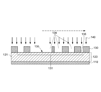
junction is no
longer planar, e.g. at a region of curvature, such as that at the periphery or
edges of
device active area.
[0003] In particular, breakdown voltage is critical for high power devices,
such as
silicon carbide (SIC) devices. Also, properties, such as insensitivity of
device design
(including termination) to active dose and interface charge variation, are
more substantial
in SIC devices, than in silicon (Si) based devices due to fundamental
structural material
differences.
[0004] Semiconductor devices may utilize any of various structures and
methods
to achieve an increase in the breakdown voltage. For example, junction
termination
extension (JTE) regions may be utilized near edge portions of the p-n junction
formed by
CA 02855304 2014-06-27
268166
active area of device. In general, a JTE region may be considered as a more
lightly doped
extension of a heavily doped semiconductor region that adjoins a lightly doped
semiconductor region having opposite type of conductivity to form the
foregoing p-n
junction. The principal function of the JTE region is to reduce the high
concentration of
electric field that would otherwise exist in the vicinity of the unterminated
portion of the
p-n junction, by laterally extending the blocking junction.
[0005] In addition to
breakdown voltage, the design of the JTE affects a number
of critical properties of the semiconductor device, including reliability and
surface charge
variation tolerance, and many of the affected properties have complex
interrelationships.
However, typical methods of manufacturing semiconductor devices include
multiple
implantation steps performed sequentially, which leads to higher implant
costs.
[0006] Accordingly,
there is a need for improved methods of manufacturing
semiconductor devices including a JTE design. Further, it may be desirable to
provide a
JTE design that improves the critical properties of silicon-carbide based
semiconductor
devices, such as breakdown voltage, charge tolerance to surface charge
variation and
reliability.
BRIEF DESCRIPTION OF THE INVENTION
[0007] One embodiment
is directed to a method of manufacturing a
semiconductor device. The method
comprises providing a semiconductor layer
comprising silicon carbide, wherein the semiconductor layer comprises a first
region
doped with a first dopant type. The method
further comprises implanting the
semiconductor layer with a second dopant type using a single implantation mask
and a
substantially similar implantation dose to form a second region and a junction
termination
extension (JTE) in the semiconductor layer, wherein the implantation dose is
in a range
from about 2 x 10¹³ em12t0 about 12 x 1013cm-2.
[0008] Another embodiment is directed to a semiconductor device. The
semiconductor device comprises a substrate and a semiconductor layer
comprising silicon
2
CA 02855304 2014-06-27
268166
carbide disposed on the substrate. The semiconductor layer comprises a first
region, a
second region, and a junction termination extension (JTE), wherein the first
region is
doped with a first dopant type to have a first conductivity type, and the
second region and
the JTE are doped with a second dopant-type to have a second conductivity
type. An
implanted dose in the second region and the JTE is in a range from about 2 x
1013 cm-2 to
about 12 x 1013 cm-2, and a dopant concentration in the second region is
substantially the
same as the dopant concentration in the JTE.
[0009] Another embodiment is directed to a semiconductor device. The
semiconductor device comprises a substrate and a semiconductor layer
comprising silicon
carbide disposed on the substrate. The semiconductor layer comprises a first
region. a
second region, and a junction termination extension (JTE), wherein the first
region is
doped with a first dopant type to have a first conductivity type, and the
second region and
the JTE are doped with a second dopant-type to have a second conductivity
type. An
implanted dose in the second region and the JTE is in a range from about 2 x
1013 ern-2 to
about 7.5 x 1013 cm-2, and a dopant concentration in the second region is
substantially the
same as the dopant concentration in the JTE.
DRAWINGS
[0010] These and other features, aspects, and advantages of the present
invention
will become better understood when the following detailed description is read
with
reference to the accompanying drawings, in which like characters represent
like parts
throughout the drawings, wherein:
[0011] FIG. 1 is a cross-sectional view schematically demonstrating a
method
step of manufacturing a semiconductor device, in accordance with some
embodiments of
the invention.
[0012] FIG. 2 is a cross-sectional view schematically demonstrating a
method
step of manufacturing a semiconductor device, in accordance with some
embodiments of
the invention.
13
CA 02855304 2014-06-27
268166
[0013] FIG. 3 is a cross-sectional view schematically demonstrating a
method
step of manufacturing a semiconductor device, in accordance with some
embodiments of
the invention.
[0014] FIG. 4 is a cross-sectional view schematically demonstrating a
method
step of manufacturing a MOSFET, in accordance with some embodiments of the
invention.
[0015] FIG. 5 is a cross-sectional view schematically demonstrating a
method
step of manufacturing a MOSFET, in accordance with some embodiments of the
invention.
[0016] FIG. 6 is a cross-sectional view schematically demonstrating a
method
step of manufacturing a MOSFET, in accordance with some embodiments of the
invention.
[0017] FIG. 7 is a cross-sectional view schematically demonstrating a
method
step of manufacturing a MOSFET, in accordance with some embodiments of the
invention.
[0018] FIG. 8 is a cross-sectional view of a semiconductor device, in
accordance
with some embodiments of the invention.
DETAILED DESCRIPTION
[0019] As discussed in detail below, some of the embodiments of the
invention
include methods of making silicon carbide (SIC) semiconductor devices
including a
junction termination extension (ITE).
[0020] Approximating language, as used herein throughout the specification
and
claims, may be applied to modify any quantitative representation that could
permissibly
vary without resulting in a change in the basic function to which it is
related.
Accordingly. a value modified by a term or terms, such as -about", and
"substantially" is
4
CA 02855304 2014-06-27
268166
not to be limited to the precise value specified. In some instances, the
approximating
language may correspond to the precision of an instrument for measuring the
value. Here
and throughout the specification and claims, range limitations may be combined
and/or
interchanged, such ranges are identified and include all the sub-ranges
contained therein
unless context or language indicates otherwise.
[0021] In the following specification and the claims, the singular forms
"a", "an"
and "the" include plural referents unless the context clearly dictates
otherwise. As used
herein, the term "or" is not meant to be exclusive and refers to at least one
of the
referenced components (for example, a region) being present and includes
instances in
which a combination of the referenced components may be present, unless the
context
clearly dictates otherwise.
[0022] As used herein, the term "layer" refers to a material disposed on at
least a
portion of an underlying surface in a continuous or discontinuous manner.
Further. the
term "layer" does not necessarily mean a uniform thickness of the disposed
material, and
the disposed material may have a uniform or a variable thickness. Furthermore,
the term
"a layer" as used herein refers to a single layer or a plurality of layers,
unless the context
clearly dictates otherwise.
[0023] As used herein, the term -disposed on" refers to layers disposed
directly in
contact with each other or indirectly by having intervening layers there
between, unless
otherwise specifically indicated. The term "adjacent- as used herein means
that the two
layers are disposed contiguously and arc in direct contact with each other.
[0024] In the present disclosure, when a layer is being described as "on"
another
layer or substrate, it is to be understood that the layers can either be
directly contacting
each other or have one (or more) layer or feature between the layers. Further.
the term
"on" describes the relative position of the layers to each other and does not
necessarily
mean "on top of" since the relative position above or below depends upon the
orientation
of the device to the viewer. Moreover, the use of "top," "bottom," "above,"
"below," and
CA 02855304 2014-06-27
268166
variations of these terms is made for convenience, and does not require any
particular
orientation of the components unless otherwise stated.
[0025] As described in detail later, a method of manufacturing a
semiconductor
device is presented. Figures 1-3 schematically represent a method for
fabricating a
semiconductor device 100, in accordance with one embodiment of the invention.
As
indicated in Fig. 1, the method includes providing a semiconductor layer 120
including
silicon carbide (SiC). The semiconductor layer includes a first region 121
doped with a
first dopant type (for example, n-type dopants) such that it has a first
conductivity type
(for example, n-type).
[0026] In sonic embodiments, the semiconductor layer 120 may he further
disposed on a substrate 110. The substrate 110 and the semiconductor layer 120
may be
n-type or p-type. For example, the semiconductor layer may be a SiC layer of
any
polytype of silicon carbide, such as 3C-SiC, 4H-SiC, or 6H-SiC polytypes. The
substrate
110 may comprise silicon carbide. In one embodiment, the substrate may be a
heavily
doped n+ SiC substrate and the SiC semiconductor layer may also be of n-type.
The
dopant concentration in the substrate may he in a range from about 1018 cin-3
to about
102] cm 3, in some embodiments. The dopant concentration in the SiC
semiconductor
device layer may be in a range from about 1014 cm-3 to about 1017 cm, in some
embodiments. In some embodiments, a buffer layer (not shown) may be further
disposed
between the substrate 110 and the semiconductor layer 120.
[0027] The semiconductor layer 120 may be epitaxially grown over the
substrate.
For example, a deposition technique such as, chemical vapor deposition (CVD)
may be
performed to form the semiconductor layer 120. In certain embodiments, the
thickness of
the semiconductor layer 120 may be in a range of about 1 micron to about 200
microns.
[0028] The method further includes, as indicated in Figures 2 and 3,
implanting
the semiconductor layer 120 with a second dopant type (for example, p-type
dopants)
using a single implantation mask 130 and a substantially similar implantation
dose 140 to
6
268166
form a second region 122 and a junction termination extension (JTE) 124 in the
semiconductor layer 120. The term "JTE" as used herein refers to a more
lightly doped
extension of a more heavily doped semiconductor region (second region) that
adjoins a
lightly doped semiconductor region having opposite type of conductivity to
form a p-n
junction. One of the functions of the JTE is to reduce the high electric field
that would
otherwise exist in the vicinity of the unterminated portion of the p-n
junction, and
especially at the device active area periphery, by laterally extending the
blocking
junction.
[0029] The second region 122 may be referred to as a "well region" in
semiconductor devices, such as, a metal¨oxide¨semiconductor field-effect
transistor
(MOSFET) or an insulated-gate bipolar transistor (IGBT). Further, in
semiconductor
devices, such as, a bipolar junction transistor (BJT) or a thyristor, the
second region 122
may also be referred to as a "base region". For purpose of further
description, the terms
"well region" and "base region" are used herein interchangeably. However, it
should be
noted that the description below is also applicable to "base region" in the
context of BJT
or thyristor.
[0030] As illustrated in Fig. 3, at least a portion of the JTE is
disposed within an
area doped simultaneously with, and contiguous with the second region 122.
This area
may be referred to as a "well-termination region" and may further include the
blocking
junction mentioned earlier. Referring again to Fig. 3, reference numeral 125
indicates the
blocking junction defined by the well region 122 in the semiconductor layer
120.
[0031] The term "single implantation mask" as used herein refers to a
single mask
used to provide the required dopant profile/dose in the active area (e.g. well
region 122)
and the required effective dose in JTE region 124. In some embodiments, the
method
may further include patterning the single implantation mask 130 on the
semiconductor
layer 120, for example, via photolithography and the dopants may be implanted
into the
semiconductor layer 120 using conventional ion implantation procedures (Fig.
2).
7
Date Recue/Date Received 2020-10-20
268166
[0032] As illustrated in Figures 2 and 3, the single implantation mask
130 further
includes a number of window regions 134 defining the well region 122 and the
JTE 124
in the semiconductor layer 120. The window regions 134 are further
characterized by an
open window density. The term "open window density" as used herein refers to
the
unmasked-to-total area ratio. The term "open window density profile" as used
herein
refers to the open window density number as a function of laterally increasing
distance
from the primary blocking junction.
[0033] In some embodiments, the plurality of window regions 134 further
include
a region 135 defining the primary blocking junction 125 in the semiconductor
layer 120,
as illustrated in Figures 2 and 3. In such instances, the open window density
of the
window regions 134 decreases laterally in a direction away from the region 135
defining
the primary blocking junction 125 (as indicated by an arrow in Fig. 2).
[0034] In some embodiments, an open window density of the window
regions
varies laterally such that an effective implanted dose varies in a range from
about 80
percent of the total implanted dose at the primary blocking junction to about
10 percent of
the total implanted dose at a terminal portion of the JTE, and more
particularly from
about 70 percent to about 10 percent.
[0035] As noted earlier, the open window density of the window regions
134
defining the JTE 124 decreases laterally. In some embodiments, the open window
density of the window regions 134 varies over a range of about 90 percent at
the primary
blocking junction 135 to about 5 percent at a terminal portion 136 of the JTE
124. More
particularly, the open window density of the window regions 134 may vary over
a range
of about 80 percent at the primary blocking junction 135 to about 10 percent
at a terminal
portion 136 of the JTE 124. Still more particularly, the open window density
of the
window regions 134 may vary over a range of about 70 percent at the primary
blocking
junction 135 to about 10 percent at a terminal portion 136 of the JTE 124.
8
Date Recue/Date Received 2020-10-20
CA 02855304 2014-06-27
268166
[0036] The term "substantially similar implantation dose" as used herein
means
that the single implantation dose used to provide the required doping profile
of the well
region 122 and the JTE 124 varies by less than about 5 percent. This is in
contrast to
typical methods used to manufacture the well region 122 and JTE 12, wherein
different
implantation masks as well as different implantation doses are employed to
vary the
dopant concentration profile in the well region and JTE. As will be
appreciated by one of
ordinary skill in the art, use of two different masks and implantation doses
leads to
increased number of process steps and increased process cost.
[0037] In some embodiments, the implantation dose is in a range from about
2 x
1013 cm-2 to about 12 x 1013 cm12. More particularly, the implantation dose
may be in a
range from about 2 x 1013 cm-2 to about 7.5 x 10'3 cm-2. Still more
particularly. the
implantation dose may be in a range From about 2 x 10¹³ CM-2 to about 5 x 10¹³
ern-2.
[0038] As will be appreciated by one of ordinary skill in the art, the
implantation
step may include one or more implantation process sub-steps, where
implantation may be
carried out using a single implantation energy/dose or using multiple ion
implantation
energies/doses, in each one of the implantation process sub-steps. However, as
noted
earlier, the implantation is performed using a single implantation mask and a
substantially
similar implantation dose to form well and JTE regions.
[0039] In some embodiments, implantation of the semiconductor layer 120
with a
second dopant type is performed at one or more implantation energy in a range
greater
than 5 keV and less than 700 keV. More particularly, implantation of the
semiconductor
layer 120 with a second dopant type may be performed at one or more
implantation
energy in a range greater than 20 keV and less than 400 keV to provide total
implantation
dose in the rage defined above.
[0040] The well region 122 and the JTE 124 may further include a single
well
structure or a number of structures, as indicated in Fig. 3. In certain
embodiments. the
9
CA 02855304 2014-06-27
268166
well region 122 includes a number of discrete well structures, and the JTE 124
includes a
number of JTE structures.
[0041] In certain embodiments, the JTE 124 includes a number of discrete
regions
that may be separated from each other (depending on effective dose in specific
JTE
region). The discrete regions in the JTE 124 are doped with the second dopant
type (for
example, p-type), such that an effective doping of the JTE decreases in a
direction away
from an edge of the primary blocking junction. Effective JTE doping (defined
by the
acceptor charge minus the donor charge in 124) may be controlled in part by
varying the
density of masked versus unmasked area during the implant. The effective JTE
dose/doping is defined as the product of the implanted dose/doping and the
spatial density
of unmasked to total area ratio (open window density). The effective JTE
doping can be
varied along the laterally increasing distance from the primary blocking
junction by
altering the unmasked to total area ratio according to open window density.
[0042] As noted earlier, the semiconductor layer 120 may be doped with a
first
dopant type to have a first conductivity type. The well region 122 and the JTE
124 may
be further doped with a second dopant type to have a second conductivity type.
For
example, the first and second conductivity types may be p-type and n-type. In
certain
embodiments, the first and second conductivity types may be n-type and p-type.
In such
instances, the method includes forming a p-well region and a p-doped JTE in
the n-type
SiC semiconductor layer. Suitable non-limiting examples of p-type dopants
include
boron, aluminum, gallium, magnesium, carbon, calcium, or combinations thereof.
Suitable non-limiting examples of n-type dopants include nitrogen, phosphorus,
arsenic,
antimony, or combinations thereof.
[0043] It should be noted that the method of manufacturing a semiconductor
device is applicable to a number of device types, depending on the specific
doping. Thus,
suitable non-limiting examples of the semiconductor device 100 include a
metal¨oxide¨
semiconductor field-effect transistor (MOSFET), an insulated-gate bipolar
transistor
CA 02855304 2014-06-27
268166
(IGBT), a bipolar junction transistor (BT), a thyristor, or a diode. In
certain
embodiments, the semiconductor device is a MOSFET.
[0044] Referring now
to Figures 4-7, a method of manufacturing a MOSFET 100
in accordance with some embodiments of the invention is presented. In such
instances,
the method may further include the step of removing the implantation mask 130,
followed by doping the semiconductor layer to form a source region 123 having
a first
conductivity type (for example, n-type), as indicated in Fig. 4. The source
region may be
formed, for example, via photolithography and ion implantation, as
contemplated earlier
for other regions.
[0045] Thereafter, a
base region (p+-region) 141 may be formed, as indicated in
Fig. 5. A drain electrode 127 may also he formed, for example, via vapor
deposition
and/or electroplating in contact with a surface of the substrate 110 opposite
to the surface
in contact with the semiconductor layer 120 (Fig. 6).
[0046] A gate
electrode 128 may also be formed on the semiconductor layer, by
first disposing an insulator layer 129 on the semiconductor layer 120,
followed by
forming the gate electrode 128 on the insulation layer 129 (Fig. 7). Suitable
non-limiting
example of the insulation layer 129 material may include silicon dioxide. A
source
electrode 126 may be formed in contact with the source region 123. for
example, via
vapor deposition and/or electroplating (Fig. 5).
[0047] As noted
earlier, conventional methods of forming p-well and JTE include
different mask sequences and implantation steps. Methods in accordance with
some
embodiments of the invention allow for use of a single implantation mask and a
substantially similar implantation dose to form the well region and JTE
simultaneously.
Thus, the process steps for well and JTE formation may be merged, which could
simplify
the overall process flow and save implantation and processing costs.
[0048] Further,
unlike in Si-based semiconductor devices, merging the JTE
implantation with well/base region implantation into a single profile or
process step in
1 I
CA 02855304 2014-06-27
268166
SiC semiconductor devices is more complex due to a number of material and
technological factors. In SiC power MOSFETs, the inversion channel mobility is
much
lower than in conventional Si MOSFETs. To lower the conduction losses, SIC
MOSFETS are typically designed with very short channels, e.g., less than 0.7
Therefore, in order to hold off premature punchthrough or drain-induced-
barrier-lowering
limited breakdown, a larger implanted dose than the critical dose is used to
form the well
regions. Also, since dopants in SiC diffuse very slowly and require very high
temperatures, ion implantation is the preferred method of forming well
regions.
Conventional ion implantation equipment are limited to energies such that the
resulting
junction depths are on the order of xj=1 flm or less. This further drives up
the required
well concentration to hold off punchthrough and obtain sufficiently low
spreading
resistances under the source region. The resulting optimum well/base region
implanted
doses tend to be multiple times larger than Qc (defined by Qc= EsEc, where Es
is the
dielectric constant and Ec is the critical field) in SiC devices. An example
SiC MOSFET
well region may be implanted with a dose of 5x1013cm-2 whereas the optimal JTE
implanted dose may be 1-2 x10 3CM-2. Embodiments of the present invention
allow for
both optimized SiC well regions and JTE regions with the same implanted dose,
while
using conventional ion implant technologies which are lower cost and typically
higher
volume capability.
[0049] In one
embodiment, a semiconductor device is presented. Fig. 8 illustrates
a semiconductor device 100, in accordance with one embodiment of the
invention. The
semiconductor device 100 includes a substrate 110 and a semiconductor layer
120
comprising silicon carbide disposed on the substrate 110. As illustrated in
Fig. 3, the
semiconductor layer 120 includes a first region 121, a second region 122, and
a JTE 124.
The first region 121 is doped with a first dopant type to have a first
conductivity type.
The second region 122 and the JTE 124 are doped with a second dopant-type to
have a
second conductivity type.
12
CA 02855304 2014-06-27
268166
[0050] In some embodiments, the first dopant type is p-type, and the second
dopant type is n-type. In other embodiments, the first dopant type is n-type,
and the
second dopant type is p-type. In such instances, the semiconductor includes a
p-type
second region 122 (also referred to as p-well region) and a p-type JTE 124 in
a
semiconductor layer 120.
[0051] The second region 122 and the JTE 124 are further characterized by
an
implanted dose and a dopant concentration. The term implanted dose as used
herein
refers to an amount of dopant that is implanted in the second region, and is
differentiated
from the term "implantation dose" that refers to the dose used for
implantation. The term
"implanted dose" as used herein refers to the integrated concentration of
dopant from a
surface of the semiconductor layer to the metallurgical junction.
[0052] In some embodiments, an implanted dose in the second region and the
JTE
is in a range from about 2 x 1013 cm-2 to about 12 x 1013 cm-2. More
particularly. the
implanted dose may be in a range from about 2 x 1013 cm-2 to about 7.5 x 10¹³
cm-2. Still
more particularly, the implanted dose may be in a range from about 2 x 10¹³ em-
2 to about
x 1013 cm-2. Further, the dopant concentration at a given point location in
the second
region is substantially the same as the dopant concentration at a given point
location in
the JTE.
[0053] As noted earlier, suitable non-limiting examples of the
semiconductor
device 100 include a metal¨oxide¨semiconductor field-effect transistor
(MOSFET), an
insulated-gate bipolar transistor (IGBT). a bipolar junction transistor (BJT),
a thyristor, or
a diode. In certain embodiments, the semiconductor device is a MOSFET. In
certain
embodiments, the semiconductor device is an IGBT.
[0054] Referring again to Fig. 7, a MOSFET 100 in accordance with some
embodiments of the invention is illustrated. The MOSFET 100 includes a
substrate 110
and a semiconductor layer 120 disposed on the substrate 110. The MOSFET 100
further
includes a gate electrode 128 disposed on a surface of the semiconductor layer
120. For
13
CA 02855304 2014-06-27
268166
example, the gate electrode 128 may be disposed on an insulator 129, which is
in direct
contact with the semiconductor layer 120, as indicated in Fig. 7. The MOSFET
100
further includes a drain electrode 127 disposed adjacent to a surface of the
substrate 110
that is opposite the surface on which the semiconductor layer 120 is disposed.
[0055] Further, as illustrated in Fig. 7, the semiconductor layer 120
includes a
first region 121 having a first conductivity type (for example, n-type); and a
second
region 122 (for example, well region) and JTE 124 having a conductivity of a
second
type (for example, p-type). The MOSFET 100 further includes a source region
123 of
first conductivity type (for example n-type) in contact with a source
electrode 126.
[0056] The appended claims are intended to claim the invention as broadly
as it
has been conceived and the examples herein presented are illustrative of
selected
embodiments from a manifold of all possible embodiments. Accordingly, it is
the
Applicants' intention that the appended claims are not to be limited by the
choice of
examples utilized to illustrate features of the present invention. As used in
the claims, the
word "comprises" and its grammatical variants logically also subtend and
include phrases
of varying and differing extent such as for example, but not limited thereto,
"consisting
essentially or and "consisting of." Where necessary, ranges have been
supplied; those
ranges are inclusive of all sub-ranges there between. It is to be expected
that variations in
these ranges will suggest themselves to a practitioner having ordinary skill
in the art and
where not already dedicated to the public, those variations should where
possible be
construed to be covered by the appended claims. It is also anticipated that
advances in
science and technology will make equivalents and substitutions possible that
are not now
contemplated by reason of the imprecision of language and these variations
should also
be construed where possible to be covered by the appended claims.
14