Language selection

Search

Patent 2855340 Summary

Third-party information liability

Some of the information on this Web page has been provided by external sources. The Government of Canada is not responsible for the accuracy, reliability or currency of the information supplied by external sources. Users wishing to rely upon this information should consult directly with the source of the information. Content provided by external sources is not subject to official languages, privacy and accessibility requirements.

Claims and Abstract availability

Any discrepancies in the text and image of the Claims and Abstract are due to differing posting times. Text of the Claims and Abstract are posted:

  • At the time the application is open to public inspection;
  • At the time of issue of the patent (grant).
(12) Patent Application: (11) CA 2855340
(54) English Title: ADAPTIVE EQUALIZATION OF IMPEDANCE MISMATCHED CARD-EDGE CONNECTIONS
(54) French Title: CORRECTION ADAPTATIVE DE CONNEXIONS ENCARTABLES PRESENTANT UNE DESADAPTATION D'IMPEDANCE
Status: Deemed Abandoned and Beyond the Period of Reinstatement - Pending Response to Notice of Disregarded Communication
Bibliographic Data
(51) International Patent Classification (IPC):
  • G02B 06/42 (2006.01)
  • H04B 10/2507 (2013.01)
(72) Inventors :
  • HOPKINS, STEVE (United States of America)
  • ISHAUG, BRIAN (United States of America)
  • MORBI, ZULFIKAR (United States of America)
  • SNIEZKO, OLEH (United States of America)
(73) Owners :
  • AURORA NETWORKS, INC.
(71) Applicants :
  • AURORA NETWORKS, INC. (United States of America)
(74) Agent: LAVERY, DE BILLY, LLP
(74) Associate agent:
(45) Issued:
(86) PCT Filing Date: 2012-11-09
(87) Open to Public Inspection: 2013-05-16
Examination requested: 2014-05-09
Availability of licence: N/A
Dedicated to the Public: N/A
(25) Language of filing: English

Patent Cooperation Treaty (PCT): Yes
(86) PCT Filing Number: PCT/US2012/064451
(87) International Publication Number: US2012064451
(85) National Entry: 2014-05-09

(30) Application Priority Data:
Application No. Country/Territory Date
13/672,712 (United States of America) 2012-11-09
61/628,923 (United States of America) 2011-11-09
61/628,933 (United States of America) 2011-11-09
61/629,028 (United States of America) 2011-11-10
61/629,029 (United States of America) 2011-11-10
61/629,030 (United States of America) 2011-11-10

Abstracts

English Abstract

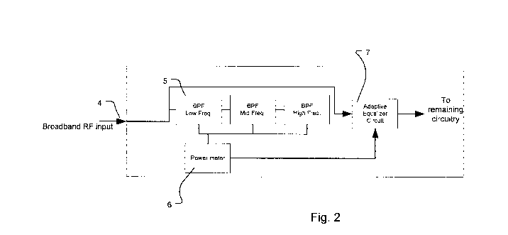
A method includes tapping power from a broadband RF input, filtering the tapped power with a plurality of band pass filters, measuring the power filtered by each of the plurality of band pass filters and controlling an adaptive equalizer circuit to flatten excessive non-linear frequency response from the broadband RF input as a function of measured power filtered at each of the plurality of band pass filters. An apparatus, includes a broadband RF input, a plurality of band pass filters coupled to the broadband RF input, at least one power measurement circuit coupled to the plurality of band pass filters and an adaptive equalizer circuit coupled to the at least one power measurement circuit and the plurality of band pass filters, wherein the at least one power measurement circuit provides control signals to the adaptive equalizer circuit as a function of measured power at each of the plurality of band pass files and wherein the adaptive equalizer circuit flattens excessive non-linear frequency response of the broadband RF input.


French Abstract

L'invention concerne un procédé comprenant les opérations consistant à dériver de l'énergie d'une entrée de radiofréquences en bande large, filtrer l'énergie dérivée avec une pluralité de filtres passe-bande, mesurer la puissance filtrée par chacun de la pluralité de filtres passe-bande et commander à un circuit égaliseur adaptatif de lisser la réponse excessive en fréquence non linéaire provenant de l'entrée de RF en bande large en fonction de l'énergie mesurée filtrée au niveau de chacun de la pluralité de filtres passe-bande. Un équipement comprend une entrée de RF en bande large, une pluralité de filtres passe-bande couplés à l'entrée de RF en bande large, au moins un circuit de mesure de puissance couplé à la pluralité de filtres passe-bande et un circuit égaliseur adaptatif couplé audit au moins un circuit de mesure de puissance et à la pluralité de filtres passe-bande, dans lequel ledit au moins un circuit de mesure de puissance envoie des signaux de commande au circuit égaliseur adaptatif en fonction de la puissance mesurée au niveau de chacun de la pluralité de filtres passe-bande et dans lequel le circuit égaliseur adaptatif lisse la réponse excessive en fréquence non linéaire de l'entrée de RF en bande large.

Claims

Note: Claims are shown in the official language in which they were submitted.


6
CLAIMS
What is claimed is:
1. A method, comprising:
tapping power from a broadband RF input,
filtering the tapped power with a plurality of band pass filters,
measuring the power filtered by each of the plurality of band pass filters and
controlling an adaptive equalizer circuit to flatten excessive non-linear
frequency
response from the broadband RF input as a function of measured power filtered
at each of
the plurality of band pass filters.
2. The method of claim 1, further comprising conveying a broadband RF
signal from a
PCB card-edge connector mating pair to the broadband RF input before tapping
power from
the broadband RF input.
3. An apparatus, comprising:
a broadband RF input,
a plurality of band pass filters coupled to the broadband RF input,
at least one power measurement circuit coupled to the plurality of band pass
filters
and
an adaptive equalizer circuit coupled to the at least one power measurement
circuit
and the plurality of band pass filters,
wherein the at least one power measurement circuit provides control signals to
the
adaptive equalizer circuit as a function of measured power at each of the
plurality of band
pass files and
wherein the adaptive equalizer circuit flattens excessive non-linear frequency
response of the broadband RF input,
4. The apparatus of claim 3, wherein the at least one power measurement
circuit
6

7
includes at least one microcontroller or logic circuit to provide control
signals to the adaptive
equalizer circuit.
5. The apparatus of claim 3, wherein the plurality of band pass filters are
connected in a
single series between the broadband RF input and the adaptive equalizer
circuit.
6. The apparatus of claim 3, wherein the at least one power measurement
circuit
includes a plurality of power measurement circuits, each of the plurality of
power
measurement circuits coupled to one of the plurality of band pass filters.
7. The apparatus of claim 3, further comprising a PCB card-edge connector
mating pair
coupled to the broadband RF input
8. A device/method substantially ai herein described.
7

Description

Note: Descriptions are shown in the official language in which they were submitted.


CA 02855340 2014-05-09
WO 2013/071108
PCT/US2012/064451
DESCRIPTION
Adaptive Equalization of Impedance Mismatched Card-Edge Connections
BACKGROUND
Broadband communication systems are complex systems with many factors to
consider
when designing RF circuits and connectors. Usually one has to use specialized
connectors
in a coaxial form-factor with proper shielding in order to mate RF connections
between
boards or modules. A problem arises when there is not enough physical space to
utilize
these RE connectors and you have to use connection methods that were not
designed for
broadband RF signals. One of the issues with using these types of non-RF
connections is
poor impedance matching that can vary each time the connections are made.
SUMMARY
There is a need for the following embodiments of the present disclosure. Of
course, the
present disclosure is not limited to these embodiments.
According to an embodiment of the present disclosure, a process comprises:
tapping power
from a broadband RF input, filtering the tapped power with a plurality of band
pass fitters,
measuring the power filtered by each of the plurality of band pass fitters and
controlling an
adaptive equalizer circuit to flatten excessive non-linear frequency response
from the
broadband RF input as a function of measured power filtered at each of the
plurality of band
pass fitters. According to another embodiment of the present disclosure, a
machine
comprises: a broadband RF input, a plurality of band pass filters coupled to
the broadband
RF input, at least one power measurement circuit coupled to the plurality of
band pass filters
and an adaptive equalizer circuit coupled to the at least one power
measurement circuit and
the plurality of band pass filters, wherein the at least one power measurement
circuit
provides control signals to the adaptive equalizer circuit as a function of
measured power at
each of the plurality of band pass files and wherein the adaptive equalizer
circuit flattens =
excessive non-linear frequency response of the broadband RF input.
These, and other, embodiments of the present disclosure will be better
appreciated and
understood when considered in conjunction with the following description and
the
accompanying drawings. It should be understood, however, that the following
description,
while indicating various embodiments of the present disclosure and numerous
specific
details thereof, is given for the purpose of illustration and does not imply
limitation. Many
1
SUBSTITUTE SHEET (RULE 26)

CA 02855340 2014-05-09
WO 2013/071108
PCT/US2012/064451
2
substitutions, modifications, additions and/or rearrangements may be made
within the scope
of embodiments of the present disclosure, and embodiments of the present
disclosure
include all such substitutions, modifications, additions and/or
rearrangements.
BRIEF DESCRIPTION OF THE DRAWINGS
The drawings accompanying and forming part of this specification are included
to depict
certain embodiments of the present disclosure. A clearer concept of the
embodiments
described in this application will be readily apparent by referring to the
exemplary, and
therefore nonlimiting, embodiments illustrated in the drawings (wherein
identical reference
numerals (if they occur in more than one view) designate the same elements).
The
described embodiments may be better understood by reference to one or more of
these
drawings in combination with the following description presented herein. It
should be noted
that the features illustrated in the drawings are not necessarily drawn to
scale.
FIG. I is block schematic view of a PCB card-edge connector mating with a card-
edge style
connector and adaptive equalizing circuit, representing an embodiment of the
present
disclosure.
FIG. 2 is block schematic view of an adaptive equalizing circuit, representing
an embodiment
of the present disclosure.
DETAILED DESCRIPTION
Embodiments presented in the present disclosure and the various features and
advantageous details thereof are explained more fully with reference to the
nonlimiting
embodiments that are illustrated in the accompanying drawings and detailed in
the following
description. Descriptions of well known signal processing techniques,
components and
equipment are omitted so as not to unnecessarily obscure the embodiments of
the present
disclosure in detail. It should be understood, however, that the detailed
description and the
specific examples are given by way of illustration only and not by way of
limitation. Various
substitutions, modifications, additions and/or rearrangements within the scope
of the
underlying inventive concept will become apparent to those skilled in the art
from this
disclosure.
Embodiments of the invention relate to transmission of analog and/or digital
signals over
fiber optics. More specifically, some embodiments of the invention relate to
small form factor
2
SUBSTITUTE SHEET (RULE 26)

CA 02855340 2014-05-09
WO 2013/071108
PCT/US2012/064451
3
pluggable modules for transmission systems such as, but not limited to, CAN
systems. The
disclosure of this application is marginally related to copending U.S. Ser.
Nos. 13/672,712,
filed November 9, 2012, 13/672,714, filed November 9, 2012, 13/672,716, filed
November 9,
2012, 13/672,717, filed November 9, 2012, 13/672,718, filed November 9, 2012
the entire
contents of all of which are hereby expressly incorporated by reference for
all purposes.
Embodiments of the invention enable the repair the symptoms of a poorly miss-
matched
connection so that cheaper and smaller form-factor connections can be
utilized, such as, but
not limited to a PCB card-edge connector mating pair.
= Embodiments of the invention can include an adaptive equalizer circuit.
Such an adaptive
equalizer circuit enables a way to fix the excessive non-linear frequency
response problems
associated with poor impedance miss-matching while using connectors that were
not
designed specifically for the job of connecting broadband RF signals.
Referring to Figure 1, a PCB card-edge connector 2 is shown mating with a card-
edge style
connector 1. The PCB card-edge connector 2 includes an adaptive equalizing
circuit 3. This
type of card-edge connector was not specifically designed for broadband analog
RF
transmissions and will have poor impedance matching characteristics. The end
result will be
a non-flat frequency response. For example, with improper impedance matching
the low
frequency signals may have higher amplitude than the higher frequency signals.
Also, the
impedance may change between mating cycles adding a new variable.
Embodiments of the invention described here will allow the use of existing
connectors not
designed for RF with PCB card-edge mating; and will adapt to the variations
one can get
with various mating cycles. Referring to Figure 2, the broadband RF input 4
injected to the
PCB card-edge connection from the connector can be tapped off and injected to
a plurality of
band pass filters (BPF) 5 and a (plurality of) Internal power measurement
circuit(s) 6. The
power measurement circuit(s) may include a microcontroller or logic circuit
that can provide
control signals to the adaptive equalizer circuits. The power
measurement/control circuit can
measure and then make adjustments to an adaptive equalizer circuit 7 in order
to flatten the
otherwise poor frequency response. The number of band pass filters can vary
from the
example shown in Figure 2 to give a finer resolution if necessary to adjust
the incoming
broadband RF input 4 signal appropriately.
3
SUBSTITUTE SHEET (RULE 26)

CA 02855340 2014-05-09
WO 2013/071108
PCT/US2012/064451
4
Definitions
The terms program and/or software and/or the phrases computer program and/or
computer
software are intended to mean a sequence of instructions designed for
execution on a
computer system (e.g., a program and/or computer program, may include a
subroutine, a
function, a procedure, an object method, an object implementation, an
executable
application, an applet, a servlet, a source code, an object code, a shared
library/dynamic
load library and/or other sequence of instructions designed for execution on a
computer or
computer system). The phrase radio frequency (RF) is intended to mean
frequencies less
than or equal to approximately 300 GHz as well as the infrared spectrum.
The term substantially is intended to mean largely but not necessarily wholly
that which is
specified. The term approximately is intended to mean at least close to a
given value (e.g.,
within 10% of). The term generally is intended to mean at least approaching a
given state.
The term coupled is intended to mean connected, although not necessarily
directly, and not
necessarily mechanically.
The terms first or one, and the phrases at least a first or at least one, are
intended to mean
the singular or the plural unless it is clear from the intrinsic text of this
document that it is
meant otherwise. The terms second or another, and the phrases at least a
second or at least
another, are intended to mean the singular or the plural unless it is clear
from the intrinsic
text of this document that it is meant otherwise. Unless expressly stated to
the contrary in
the intrinoic text of this document, the term or is intended to mean an
inclusive or and not an
exclusive or. Specifically, a condition A or B is satisfied by any one of the
following: A is true
(or present) and B is false (or not present), A is false (or not present) and
B is true (or
present), and both A and B are true (or present). The terms a and/or an are
employed for
grammatical style and merely for convenience.
The term plurality is intended to mean two or more than two. The term any is
intended to
mean all applicable members of a set or at least a subset of all applicable
members of the
set. The term means, when followed by the term 'for" is intended to mean
hardware,
firmware and/or software for achieving a result. The term step, when followed
by the term
"for is intended to mean a (sub)method, (sub)process and/or (sub)routine for
achieving the
recited.result. Unless otherwise defined, all technical and scientific terms
used herein have
the same meaning as commonly understood by one of ordinary skill in the art to
which this
present disclosure belongs. In case of conflict, the present specification,
including
definitions, will control.
The described embodiments and examples are illustrative only and not intended
to be
limiting. Although embodiments of the present disclosure can be implemented
separately,
4
SUBSTITUTE SHEET (RULE 26)

CA 02855340 2014-05-09
WO 2013/071108
PCT/US2012/064451
embodiments of the present disclosure may be integrated into the system(s)
with which they
are associated. All the embodiments of the present disclosure disclosed herein
can be made
and used without undue experimentation in light of the disclosure. Embodiments
of the
present disclosure are not limited by theoretical statements (if any) recited
herein. The
5 individual steps of embodiments of the present disclosure need not be
performed in the
disclosed manner, or combined in the disclosed sequences, but may be performed
in any
and all manner and/or combined in any and all sequences. The individual
components of
embodiments of the present disclosure need not be combined in the disclosed
configurations, but could be combined in any and all configurations.
Various substitutions, modifications, additions and/or rearrangements of the
features of
embodiments of the present disclosure may be made without deviating from the
scope of the
underlying inventive concept. All the disclosed elements and features of each
disclosed
embodiment can be combined with, or substituted for, the disclosed elements
and features
of every other disclosed embodiment except where such elements or features are
mutually
exclusive. The scope of the underlying inventive concept as defined by the
appended claims
and their equivalents cover all such substitutions, modifications, additions
and/or
rearrangements.
The appended claims are not to be interpreted as including means-plus-function
limitations,
unless such a limitation is explicitly recited in a given claim using the
phrase(s) "means for"
and/or "step for." Subgeneric embodiments of the invention are delineated by
the appended
independent claims and their equivalents. Specific embodiments of the
invention are
differentiated by the appended dependent claims and their equivalents.
5
SUBSTITUTE SHEET (RULE 26)

Representative Drawing
A single figure which represents the drawing illustrating the invention.
Administrative Status

2024-08-01:As part of the Next Generation Patents (NGP) transition, the Canadian Patents Database (CPD) now contains a more detailed Event History, which replicates the Event Log of our new back-office solution.

Please note that "Inactive:" events refers to events no longer in use in our new back-office solution.

For a clearer understanding of the status of the application/patent presented on this page, the site Disclaimer , as well as the definitions for Patent , Event History , Maintenance Fee  and Payment History  should be consulted.

Event History

Description Date
Application Not Reinstated by Deadline 2016-11-09
Time Limit for Reversal Expired 2016-11-09
Inactive: Abandoned - No reply to s.30(2) Rules requisition 2016-05-02
Deemed Abandoned - Failure to Respond to Maintenance Fee Notice 2015-11-09
Inactive: S.30(2) Rules - Examiner requisition 2015-10-30
Inactive: Report - No QC 2015-09-29
Letter Sent 2014-08-07
Inactive: Reply to s.37 Rules - PCT 2014-07-30
Inactive: Single transfer 2014-07-30
Inactive: Cover page published 2014-07-30
Inactive: Request under s.37 Rules - PCT 2014-07-04
Application Received - PCT 2014-07-04
Inactive: First IPC assigned 2014-07-04
Inactive: IPC assigned 2014-07-04
Inactive: Acknowledgment of national entry - RFE 2014-07-04
Letter Sent 2014-07-04
Request for Examination Requirements Determined Compliant 2014-05-09
All Requirements for Examination Determined Compliant 2014-05-09
National Entry Requirements Determined Compliant 2014-05-09
Application Published (Open to Public Inspection) 2013-05-16

Abandonment History

Abandonment Date Reason Reinstatement Date
2015-11-09

Maintenance Fee

The last payment was received on 2014-10-20

Note : If the full payment has not been received on or before the date indicated, a further fee may be required which may be one of the following

  • the reinstatement fee;
  • the late payment fee; or
  • additional fee to reverse deemed expiry.

Patent fees are adjusted on the 1st of January every year. The amounts above are the current amounts if received by December 31 of the current year.
Please refer to the CIPO Patent Fees web page to see all current fee amounts.

Fee History

Fee Type Anniversary Year Due Date Paid Date
Request for examination - standard 2014-05-09
Basic national fee - standard 2014-05-09
Registration of a document 2014-07-30
MF (application, 2nd anniv.) - standard 02 2014-11-10 2014-10-20
Owners on Record

Note: Records showing the ownership history in alphabetical order.

Current Owners on Record
AURORA NETWORKS, INC.
Past Owners on Record
BRIAN ISHAUG
OLEH SNIEZKO
STEVE HOPKINS
ZULFIKAR MORBI
Past Owners that do not appear in the "Owners on Record" listing will appear in other documentation within the application.
Documents

To view selected files, please enter reCAPTCHA code :


To view images, click a link in the Document Description column. To download the documents, select one or more checkboxes in the first column and then click the "Download Selected in PDF format (Zip Archive)" or the "Download Selected as Single PDF" button.

List of published and non-published patent-specific documents on the CPD .

If you have any difficulty accessing content, you can call the Client Service Centre at 1-866-997-1936 or send them an e-mail at CIPO Client Service Centre.


Document
Description 
Date
(yyyy-mm-dd) 
Number of pages   Size of Image (KB) 
Description 2014-05-08 5 249
Representative drawing 2014-05-08 1 6
Claims 2014-05-08 2 45
Drawings 2014-05-08 2 15
Abstract 2014-05-08 1 72
Acknowledgement of Request for Examination 2014-07-03 1 175
Reminder of maintenance fee due 2014-07-09 1 110
Notice of National Entry 2014-07-03 1 201
Courtesy - Certificate of registration (related document(s)) 2014-08-06 1 104
Courtesy - Abandonment Letter (Maintenance Fee) 2015-12-20 1 172
Courtesy - Abandonment Letter (R30(2)) 2016-06-12 1 164
PCT 2014-05-08 22 814
Correspondence 2014-07-29 8 323
Examiner Requisition 2015-10-29 3 229