Sélection de la langue

Search

Sommaire du brevet 2855340 

Énoncé de désistement de responsabilité concernant l'information provenant de tiers

Une partie des informations de ce site Web a été fournie par des sources externes. Le gouvernement du Canada n'assume aucune responsabilité concernant la précision, l'actualité ou la fiabilité des informations fournies par les sources externes. Les utilisateurs qui désirent employer cette information devraient consulter directement la source des informations. Le contenu fourni par les sources externes n'est pas assujetti aux exigences sur les langues officielles, la protection des renseignements personnels et l'accessibilité.

Disponibilité de l'Abrégé et des Revendications

L'apparition de différences dans le texte et l'image des Revendications et de l'Abrégé dépend du moment auquel le document est publié. Les textes des Revendications et de l'Abrégé sont affichés :

  • lorsque la demande peut être examinée par le public;
  • lorsque le brevet est émis (délivrance).
(12) Demande de brevet: (11) CA 2855340
(54) Titre français: CORRECTION ADAPTATIVE DE CONNEXIONS ENCARTABLES PRESENTANT UNE DESADAPTATION D'IMPEDANCE
(54) Titre anglais: ADAPTIVE EQUALIZATION OF IMPEDANCE MISMATCHED CARD-EDGE CONNECTIONS
Statut: Réputée abandonnée et au-delà du délai pour le rétablissement - en attente de la réponse à l’avis de communication rejetée
Données bibliographiques
(51) Classification internationale des brevets (CIB):
  • G02B 06/42 (2006.01)
  • H04B 10/2507 (2013.01)
(72) Inventeurs :
  • HOPKINS, STEVE (Etats-Unis d'Amérique)
  • ISHAUG, BRIAN (Etats-Unis d'Amérique)
  • MORBI, ZULFIKAR (Etats-Unis d'Amérique)
  • SNIEZKO, OLEH (Etats-Unis d'Amérique)
(73) Titulaires :
  • AURORA NETWORKS, INC.
(71) Demandeurs :
  • AURORA NETWORKS, INC. (Etats-Unis d'Amérique)
(74) Agent: LAVERY, DE BILLY, LLP
(74) Co-agent:
(45) Délivré:
(86) Date de dépôt PCT: 2012-11-09
(87) Mise à la disponibilité du public: 2013-05-16
Requête d'examen: 2014-05-09
Licence disponible: S.O.
Cédé au domaine public: S.O.
(25) Langue des documents déposés: Anglais

Traité de coopération en matière de brevets (PCT): Oui
(86) Numéro de la demande PCT: PCT/US2012/064451
(87) Numéro de publication internationale PCT: US2012064451
(85) Entrée nationale: 2014-05-09

(30) Données de priorité de la demande:
Numéro de la demande Pays / territoire Date
13/672,712 (Etats-Unis d'Amérique) 2012-11-09
61/628,923 (Etats-Unis d'Amérique) 2011-11-09
61/628,933 (Etats-Unis d'Amérique) 2011-11-09
61/629,028 (Etats-Unis d'Amérique) 2011-11-10
61/629,029 (Etats-Unis d'Amérique) 2011-11-10
61/629,030 (Etats-Unis d'Amérique) 2011-11-10

Abrégés

Abrégé français

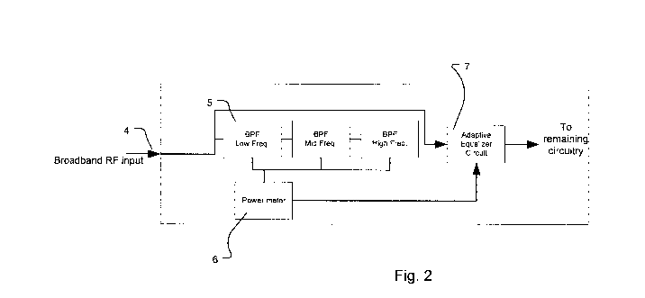
L'invention concerne un procédé comprenant les opérations consistant à dériver de l'énergie d'une entrée de radiofréquences en bande large, filtrer l'énergie dérivée avec une pluralité de filtres passe-bande, mesurer la puissance filtrée par chacun de la pluralité de filtres passe-bande et commander à un circuit égaliseur adaptatif de lisser la réponse excessive en fréquence non linéaire provenant de l'entrée de RF en bande large en fonction de l'énergie mesurée filtrée au niveau de chacun de la pluralité de filtres passe-bande. Un équipement comprend une entrée de RF en bande large, une pluralité de filtres passe-bande couplés à l'entrée de RF en bande large, au moins un circuit de mesure de puissance couplé à la pluralité de filtres passe-bande et un circuit égaliseur adaptatif couplé audit au moins un circuit de mesure de puissance et à la pluralité de filtres passe-bande, dans lequel ledit au moins un circuit de mesure de puissance envoie des signaux de commande au circuit égaliseur adaptatif en fonction de la puissance mesurée au niveau de chacun de la pluralité de filtres passe-bande et dans lequel le circuit égaliseur adaptatif lisse la réponse excessive en fréquence non linéaire de l'entrée de RF en bande large.


Abrégé anglais

A method includes tapping power from a broadband RF input, filtering the tapped power with a plurality of band pass filters, measuring the power filtered by each of the plurality of band pass filters and controlling an adaptive equalizer circuit to flatten excessive non-linear frequency response from the broadband RF input as a function of measured power filtered at each of the plurality of band pass filters. An apparatus, includes a broadband RF input, a plurality of band pass filters coupled to the broadband RF input, at least one power measurement circuit coupled to the plurality of band pass filters and an adaptive equalizer circuit coupled to the at least one power measurement circuit and the plurality of band pass filters, wherein the at least one power measurement circuit provides control signals to the adaptive equalizer circuit as a function of measured power at each of the plurality of band pass files and wherein the adaptive equalizer circuit flattens excessive non-linear frequency response of the broadband RF input.

Revendications

Note : Les revendications sont présentées dans la langue officielle dans laquelle elles ont été soumises.


6
CLAIMS
What is claimed is:
1. A method, comprising:
tapping power from a broadband RF input,
filtering the tapped power with a plurality of band pass filters,
measuring the power filtered by each of the plurality of band pass filters and
controlling an adaptive equalizer circuit to flatten excessive non-linear
frequency
response from the broadband RF input as a function of measured power filtered
at each of
the plurality of band pass filters.
2. The method of claim 1, further comprising conveying a broadband RF
signal from a
PCB card-edge connector mating pair to the broadband RF input before tapping
power from
the broadband RF input.
3. An apparatus, comprising:
a broadband RF input,
a plurality of band pass filters coupled to the broadband RF input,
at least one power measurement circuit coupled to the plurality of band pass
filters
and
an adaptive equalizer circuit coupled to the at least one power measurement
circuit
and the plurality of band pass filters,
wherein the at least one power measurement circuit provides control signals to
the
adaptive equalizer circuit as a function of measured power at each of the
plurality of band
pass files and
wherein the adaptive equalizer circuit flattens excessive non-linear frequency
response of the broadband RF input,
4. The apparatus of claim 3, wherein the at least one power measurement
circuit
6

7
includes at least one microcontroller or logic circuit to provide control
signals to the adaptive
equalizer circuit.
5. The apparatus of claim 3, wherein the plurality of band pass filters are
connected in a
single series between the broadband RF input and the adaptive equalizer
circuit.
6. The apparatus of claim 3, wherein the at least one power measurement
circuit
includes a plurality of power measurement circuits, each of the plurality of
power
measurement circuits coupled to one of the plurality of band pass filters.
7. The apparatus of claim 3, further comprising a PCB card-edge connector
mating pair
coupled to the broadband RF input
8. A device/method substantially ai herein described.
7

Description

Note : Les descriptions sont présentées dans la langue officielle dans laquelle elles ont été soumises.


CA 02855340 2014-05-09
WO 2013/071108
PCT/US2012/064451
DESCRIPTION
Adaptive Equalization of Impedance Mismatched Card-Edge Connections
BACKGROUND
Broadband communication systems are complex systems with many factors to
consider
when designing RF circuits and connectors. Usually one has to use specialized
connectors
in a coaxial form-factor with proper shielding in order to mate RF connections
between
boards or modules. A problem arises when there is not enough physical space to
utilize
these RE connectors and you have to use connection methods that were not
designed for
broadband RF signals. One of the issues with using these types of non-RF
connections is
poor impedance matching that can vary each time the connections are made.
SUMMARY
There is a need for the following embodiments of the present disclosure. Of
course, the
present disclosure is not limited to these embodiments.
According to an embodiment of the present disclosure, a process comprises:
tapping power
from a broadband RF input, filtering the tapped power with a plurality of band
pass fitters,
measuring the power filtered by each of the plurality of band pass fitters and
controlling an
adaptive equalizer circuit to flatten excessive non-linear frequency response
from the
broadband RF input as a function of measured power filtered at each of the
plurality of band
pass fitters. According to another embodiment of the present disclosure, a
machine
comprises: a broadband RF input, a plurality of band pass filters coupled to
the broadband
RF input, at least one power measurement circuit coupled to the plurality of
band pass filters
and an adaptive equalizer circuit coupled to the at least one power
measurement circuit and
the plurality of band pass filters, wherein the at least one power measurement
circuit
provides control signals to the adaptive equalizer circuit as a function of
measured power at
each of the plurality of band pass files and wherein the adaptive equalizer
circuit flattens =
excessive non-linear frequency response of the broadband RF input.
These, and other, embodiments of the present disclosure will be better
appreciated and
understood when considered in conjunction with the following description and
the
accompanying drawings. It should be understood, however, that the following
description,
while indicating various embodiments of the present disclosure and numerous
specific
details thereof, is given for the purpose of illustration and does not imply
limitation. Many
1
SUBSTITUTE SHEET (RULE 26)

CA 02855340 2014-05-09
WO 2013/071108
PCT/US2012/064451
2
substitutions, modifications, additions and/or rearrangements may be made
within the scope
of embodiments of the present disclosure, and embodiments of the present
disclosure
include all such substitutions, modifications, additions and/or
rearrangements.
BRIEF DESCRIPTION OF THE DRAWINGS
The drawings accompanying and forming part of this specification are included
to depict
certain embodiments of the present disclosure. A clearer concept of the
embodiments
described in this application will be readily apparent by referring to the
exemplary, and
therefore nonlimiting, embodiments illustrated in the drawings (wherein
identical reference
numerals (if they occur in more than one view) designate the same elements).
The
described embodiments may be better understood by reference to one or more of
these
drawings in combination with the following description presented herein. It
should be noted
that the features illustrated in the drawings are not necessarily drawn to
scale.
FIG. I is block schematic view of a PCB card-edge connector mating with a card-
edge style
connector and adaptive equalizing circuit, representing an embodiment of the
present
disclosure.
FIG. 2 is block schematic view of an adaptive equalizing circuit, representing
an embodiment
of the present disclosure.
DETAILED DESCRIPTION
Embodiments presented in the present disclosure and the various features and
advantageous details thereof are explained more fully with reference to the
nonlimiting
embodiments that are illustrated in the accompanying drawings and detailed in
the following
description. Descriptions of well known signal processing techniques,
components and
equipment are omitted so as not to unnecessarily obscure the embodiments of
the present
disclosure in detail. It should be understood, however, that the detailed
description and the
specific examples are given by way of illustration only and not by way of
limitation. Various
substitutions, modifications, additions and/or rearrangements within the scope
of the
underlying inventive concept will become apparent to those skilled in the art
from this
disclosure.
Embodiments of the invention relate to transmission of analog and/or digital
signals over
fiber optics. More specifically, some embodiments of the invention relate to
small form factor
2
SUBSTITUTE SHEET (RULE 26)

CA 02855340 2014-05-09
WO 2013/071108
PCT/US2012/064451
3
pluggable modules for transmission systems such as, but not limited to, CAN
systems. The
disclosure of this application is marginally related to copending U.S. Ser.
Nos. 13/672,712,
filed November 9, 2012, 13/672,714, filed November 9, 2012, 13/672,716, filed
November 9,
2012, 13/672,717, filed November 9, 2012, 13/672,718, filed November 9, 2012
the entire
contents of all of which are hereby expressly incorporated by reference for
all purposes.
Embodiments of the invention enable the repair the symptoms of a poorly miss-
matched
connection so that cheaper and smaller form-factor connections can be
utilized, such as, but
not limited to a PCB card-edge connector mating pair.
= Embodiments of the invention can include an adaptive equalizer circuit.
Such an adaptive
equalizer circuit enables a way to fix the excessive non-linear frequency
response problems
associated with poor impedance miss-matching while using connectors that were
not
designed specifically for the job of connecting broadband RF signals.
Referring to Figure 1, a PCB card-edge connector 2 is shown mating with a card-
edge style
connector 1. The PCB card-edge connector 2 includes an adaptive equalizing
circuit 3. This
type of card-edge connector was not specifically designed for broadband analog
RF
transmissions and will have poor impedance matching characteristics. The end
result will be
a non-flat frequency response. For example, with improper impedance matching
the low
frequency signals may have higher amplitude than the higher frequency signals.
Also, the
impedance may change between mating cycles adding a new variable.
Embodiments of the invention described here will allow the use of existing
connectors not
designed for RF with PCB card-edge mating; and will adapt to the variations
one can get
with various mating cycles. Referring to Figure 2, the broadband RF input 4
injected to the
PCB card-edge connection from the connector can be tapped off and injected to
a plurality of
band pass filters (BPF) 5 and a (plurality of) Internal power measurement
circuit(s) 6. The
power measurement circuit(s) may include a microcontroller or logic circuit
that can provide
control signals to the adaptive equalizer circuits. The power
measurement/control circuit can
measure and then make adjustments to an adaptive equalizer circuit 7 in order
to flatten the
otherwise poor frequency response. The number of band pass filters can vary
from the
example shown in Figure 2 to give a finer resolution if necessary to adjust
the incoming
broadband RF input 4 signal appropriately.
3
SUBSTITUTE SHEET (RULE 26)

CA 02855340 2014-05-09
WO 2013/071108
PCT/US2012/064451
4
Definitions
The terms program and/or software and/or the phrases computer program and/or
computer
software are intended to mean a sequence of instructions designed for
execution on a
computer system (e.g., a program and/or computer program, may include a
subroutine, a
function, a procedure, an object method, an object implementation, an
executable
application, an applet, a servlet, a source code, an object code, a shared
library/dynamic
load library and/or other sequence of instructions designed for execution on a
computer or
computer system). The phrase radio frequency (RF) is intended to mean
frequencies less
than or equal to approximately 300 GHz as well as the infrared spectrum.
The term substantially is intended to mean largely but not necessarily wholly
that which is
specified. The term approximately is intended to mean at least close to a
given value (e.g.,
within 10% of). The term generally is intended to mean at least approaching a
given state.
The term coupled is intended to mean connected, although not necessarily
directly, and not
necessarily mechanically.
The terms first or one, and the phrases at least a first or at least one, are
intended to mean
the singular or the plural unless it is clear from the intrinsic text of this
document that it is
meant otherwise. The terms second or another, and the phrases at least a
second or at least
another, are intended to mean the singular or the plural unless it is clear
from the intrinsic
text of this document that it is meant otherwise. Unless expressly stated to
the contrary in
the intrinoic text of this document, the term or is intended to mean an
inclusive or and not an
exclusive or. Specifically, a condition A or B is satisfied by any one of the
following: A is true
(or present) and B is false (or not present), A is false (or not present) and
B is true (or
present), and both A and B are true (or present). The terms a and/or an are
employed for
grammatical style and merely for convenience.
The term plurality is intended to mean two or more than two. The term any is
intended to
mean all applicable members of a set or at least a subset of all applicable
members of the
set. The term means, when followed by the term 'for" is intended to mean
hardware,
firmware and/or software for achieving a result. The term step, when followed
by the term
"for is intended to mean a (sub)method, (sub)process and/or (sub)routine for
achieving the
recited.result. Unless otherwise defined, all technical and scientific terms
used herein have
the same meaning as commonly understood by one of ordinary skill in the art to
which this
present disclosure belongs. In case of conflict, the present specification,
including
definitions, will control.
The described embodiments and examples are illustrative only and not intended
to be
limiting. Although embodiments of the present disclosure can be implemented
separately,
4
SUBSTITUTE SHEET (RULE 26)

CA 02855340 2014-05-09
WO 2013/071108
PCT/US2012/064451
embodiments of the present disclosure may be integrated into the system(s)
with which they
are associated. All the embodiments of the present disclosure disclosed herein
can be made
and used without undue experimentation in light of the disclosure. Embodiments
of the
present disclosure are not limited by theoretical statements (if any) recited
herein. The
5 individual steps of embodiments of the present disclosure need not be
performed in the
disclosed manner, or combined in the disclosed sequences, but may be performed
in any
and all manner and/or combined in any and all sequences. The individual
components of
embodiments of the present disclosure need not be combined in the disclosed
configurations, but could be combined in any and all configurations.
Various substitutions, modifications, additions and/or rearrangements of the
features of
embodiments of the present disclosure may be made without deviating from the
scope of the
underlying inventive concept. All the disclosed elements and features of each
disclosed
embodiment can be combined with, or substituted for, the disclosed elements
and features
of every other disclosed embodiment except where such elements or features are
mutually
exclusive. The scope of the underlying inventive concept as defined by the
appended claims
and their equivalents cover all such substitutions, modifications, additions
and/or
rearrangements.
The appended claims are not to be interpreted as including means-plus-function
limitations,
unless such a limitation is explicitly recited in a given claim using the
phrase(s) "means for"
and/or "step for." Subgeneric embodiments of the invention are delineated by
the appended
independent claims and their equivalents. Specific embodiments of the
invention are
differentiated by the appended dependent claims and their equivalents.
5
SUBSTITUTE SHEET (RULE 26)

Dessin représentatif
Une figure unique qui représente un dessin illustrant l'invention.
États administratifs

2024-08-01 : Dans le cadre de la transition vers les Brevets de nouvelle génération (BNG), la base de données sur les brevets canadiens (BDBC) contient désormais un Historique d'événement plus détaillé, qui reproduit le Journal des événements de notre nouvelle solution interne.

Veuillez noter que les événements débutant par « Inactive : » se réfèrent à des événements qui ne sont plus utilisés dans notre nouvelle solution interne.

Pour une meilleure compréhension de l'état de la demande ou brevet qui figure sur cette page, la rubrique Mise en garde , et les descriptions de Brevet , Historique d'événement , Taxes périodiques et Historique des paiements devraient être consultées.

Historique d'événement

Description Date
Demande non rétablie avant l'échéance 2016-11-09
Le délai pour l'annulation est expiré 2016-11-09
Inactive : Abandon. - Aucune rép dem par.30(2) Règles 2016-05-02
Réputée abandonnée - omission de répondre à un avis sur les taxes pour le maintien en état 2015-11-09
Inactive : Dem. de l'examinateur par.30(2) Règles 2015-10-30
Inactive : Rapport - Aucun CQ 2015-09-29
Lettre envoyée 2014-08-07
Inactive : Réponse à l'art.37 Règles - PCT 2014-07-30
Inactive : Transfert individuel 2014-07-30
Inactive : Page couverture publiée 2014-07-30
Inactive : Demande sous art.37 Règles - PCT 2014-07-04
Demande reçue - PCT 2014-07-04
Inactive : CIB en 1re position 2014-07-04
Inactive : CIB attribuée 2014-07-04
Inactive : Acc. récept. de l'entrée phase nat. - RE 2014-07-04
Lettre envoyée 2014-07-04
Exigences pour une requête d'examen - jugée conforme 2014-05-09
Toutes les exigences pour l'examen - jugée conforme 2014-05-09
Exigences pour l'entrée dans la phase nationale - jugée conforme 2014-05-09
Demande publiée (accessible au public) 2013-05-16

Historique d'abandonnement

Date d'abandonnement Raison Date de rétablissement
2015-11-09

Taxes périodiques

Le dernier paiement a été reçu le 2014-10-20

Avis : Si le paiement en totalité n'a pas été reçu au plus tard à la date indiquée, une taxe supplémentaire peut être imposée, soit une des taxes suivantes :

  • taxe de rétablissement ;
  • taxe pour paiement en souffrance ; ou
  • taxe additionnelle pour le renversement d'une péremption réputée.

Les taxes sur les brevets sont ajustées au 1er janvier de chaque année. Les montants ci-dessus sont les montants actuels s'ils sont reçus au plus tard le 31 décembre de l'année en cours.
Veuillez vous référer à la page web des taxes sur les brevets de l'OPIC pour voir tous les montants actuels des taxes.

Historique des taxes

Type de taxes Anniversaire Échéance Date payée
Requête d'examen - générale 2014-05-09
Taxe nationale de base - générale 2014-05-09
Enregistrement d'un document 2014-07-30
TM (demande, 2e anniv.) - générale 02 2014-11-10 2014-10-20
Titulaires au dossier

Les titulaires actuels et antérieures au dossier sont affichés en ordre alphabétique.

Titulaires actuels au dossier
AURORA NETWORKS, INC.
Titulaires antérieures au dossier
BRIAN ISHAUG
OLEH SNIEZKO
STEVE HOPKINS
ZULFIKAR MORBI
Les propriétaires antérieurs qui ne figurent pas dans la liste des « Propriétaires au dossier » apparaîtront dans d'autres documents au dossier.
Documents

Pour visionner les fichiers sélectionnés, entrer le code reCAPTCHA :


Pour visualiser une image, cliquer sur un lien dans la colonne description du document. Pour télécharger l'image (les images), cliquer l'une ou plusieurs cases à cocher dans la première colonne et ensuite cliquer sur le bouton "Télécharger sélection en format PDF (archive Zip)" ou le bouton "Télécharger sélection (en un fichier PDF fusionné)".

Liste des documents de brevet publiés et non publiés sur la BDBC .

Si vous avez des difficultés à accéder au contenu, veuillez communiquer avec le Centre de services à la clientèle au 1-866-997-1936, ou envoyer un courriel au Centre de service à la clientèle de l'OPIC.


Description du
Document 
Date
(aaaa-mm-jj) 
Nombre de pages   Taille de l'image (Ko) 
Description 2014-05-08 5 249
Dessin représentatif 2014-05-08 1 6
Revendications 2014-05-08 2 45
Dessins 2014-05-08 2 15
Abrégé 2014-05-08 1 72
Accusé de réception de la requête d'examen 2014-07-03 1 175
Rappel de taxe de maintien due 2014-07-09 1 110
Avis d'entree dans la phase nationale 2014-07-03 1 201
Courtoisie - Certificat d'enregistrement (document(s) connexe(s)) 2014-08-06 1 104
Courtoisie - Lettre d'abandon (taxe de maintien en état) 2015-12-20 1 172
Courtoisie - Lettre d'abandon (R30(2)) 2016-06-12 1 164
PCT 2014-05-08 22 814
Correspondance 2014-07-29 8 323
Demande de l'examinateur 2015-10-29 3 229