Note: Descriptions are shown in the official language in which they were submitted.
81779212
INTERDIGITATED ARRAY AND METHOD OF MANUFACTURE
Cross-Reference to Related Applications
[0001] This application claims the benefit of US Serial No. 61/562,645,
filed
November 22, 2011 and of US Serial No. 61/577,933 filed December 20, 2011.
Statement regarding Federally Sponsored Research and Development
[0002] Not Applicable.
Background
[0003] A sensor (also called detector) is a device that measures a
physical quantity and converts it into a signal which can be read by an
observer or by an instrument. For example, a mercury-in-glass thermometer
converts the measured temperature into expansion and contraction of a liquid
which can be read on a calibrated glass tube. A thermocouple converts
temperature to an output voltage which can be read by a voltmeter. For
accuracy, most sensors are calibrated against known standards.
[0004] In biomedicine and biotechnology, sensors which detect
analytes having a biological component, such as cells, protein, or nucleic
acid
are called biosensors. Biosensors can be used for both in vitro and in vivo
applications.
[0005] Typically, biosensors are exposed to a biological specimen,
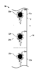
such as blood or urine and are used to detect predetermined analytes within
the biological specimen. The biosensor may then be exposed to a transducer
or detector element which may work in a physiochemical manner using a
1
CA 2856380 2019-02-06
CA 02856380 2014-05-20
WO 2013/078127
PCT/US2012/065834
sensing medium such as light, electricity, piezoelectric, electrochemical or
the
like. In any event, the transducer or detector element transforms a signal
from
the biosensor into another signal that can be more easily measured and
quantified. The signal produced by the transducer or detector element may
be provided to a reader device having associated electronics, signal
processors and/or a display to provide the results in a user readable format.
For example, the results can be provided on a graphical display.
[0006] In any event, one type of biosensor that has been used in the
past is based upon technology including an interdigitated sensor array which
achieves amplification of a sensor signal. The interdigitated sensor array is
provided with at least two microelectrodes, both of which have fingers which
are spaced apart and interleaved in an interdigitated fashion. Each of the
microelectrodes is provided with a relatively large trace connected to a
plurality of relatively fine traces. Exemplary interdigitated sensor arrays
have
been described in a variety of articles, such as Large-area interdigitated
array
microelectrodes for electrochemical sensing, Sensors and Actuators, Adam E.
Cohen, and Roderick R. Kunz (2000) pgs. 23-29; Digital Simulation of the
Measured Electrochemical Response of Reversible Redox Couples at
Microelectrode Arrays: Consequences Arising from Closely Spaced
Ultramicroelectrodes, Allen J. Bard et al., Anal. Chem. 1986, 58, 2321-2331;
and United States Patent Application Number 2009/0084686, filed on
February 27, 2008; and United States Patent Application Number
2007/0145356, filed on December 25, 2005.
[0007] Limitations in the trace dimensions (the width of the
interdigitated fingers) and space dimensions (the edge-to-edge distance of the
2
= 81779212
interdigitated fingers) are encountered using standard screen printing,
electrodeposition and laser ablation approaches to manufacturing the
interdigitated sensor arrays. For these reasons, in the past, the
interdigitated
sensor arrays have been fabricated using semi-conductor type fabrication
techniques including photolithography using substrates suitable for use in
semiconductor fabrication. Exemplary prior art substrates include silicon
dioxide,
glass, ceramic, a semiconductor material, or a flexible material. See for
example,
paragraph [0023] of United States Patent Application Number 2007/0145356.
[0008] However, to Applicant's knowledge, there has not been a cost-effective
method for fabricating a biosensor with an interdigitated sensor array that
makes
such biosensor available to be mass produced and widely used as a disposable
sensor for testing biological specimens, such as blood and urine. It is to
such a
method and apparatus for cost-effectively producing biosensors that the
present
disclosure is directed.
SUMMARY
[0008a] According to one aspect of the present invention, there is provided a
method of making a sensor card, comprising the steps of: applying a first
conductive
ink to a substrate in a first pattern to form a first conducting element and a
second
conducting element, the first and second conducting elements having first and
second widths, the first conductive ink having a particle size of greater than
5
microns; applying a second conductive ink to the substrate with an aerosol
jetting
apparatus in a second pattern to form first fingers interleaved with second
fingers, the
first and second fingers having third and fourth widths that are less than the
first and
second widths of the first and second conducting element, the first fingers
being
spaced a distance from the second fingers between 10 nanometers and 1
millimeter,
the second conductive ink having a particle size of less than or equal to 5
microns,
wherein the first conducting element and the first fingers are electrically
connected to
form a first electrode of a sensor unit, and the second conducting element are
3
CA 2856380 2019-02-06
81779212
electrically connected to the second fingers to form a second electrode of the
sensor
unit; and wherein the step of applying the first conductive ink to the
substrate is
defined further as applying the first conductive ink to the substrate
utilizing a non-
aerosol jetting apparatus selected from a group consisting of a screen
printing
apparatus, a stenciling apparatus, an electro-deposition apparatus, a
sputtering
apparatus, a jetting apparatus, a laser ablation apparatus and combinations
thereof;
and further comprising the step of applying sensor-immobilized biomolecule
receptors
on the substrate between the first electrode and the second electrode such
that the
first electrode is electrically connected to the second electrode upon one or
more of
the biomolecule receptors binding to a biomolecule.
BRIEF DESCRIPTION OF THE DRAWINGS
[0009] The accompanying drawings, which are incorporated in and constitute a
part of this specification, illustrate one or more implementations described
herein and,
together with the description, explain these implementations. In the drawings:
[0010] Figure 1 is a partial, top plan view of a web product having a
plurality of card
zones defining sensing areas with sensor units formed within the sensing areas
in
accordance with the present disclosure.
3a
CA 2856380 2019-02-06
CA 02856380 2014-05-20
WO 2013/078127
PCT/US2012/065834
[0011] Figure 2 is a top plan view of an exemplary sensor card
constructed in accordance with the present disclosure.
[0012] Figure 3 is a top plan view of an exemplary sensor unit
constructed in accordance with the present disclosure.
[0013] Figures 4a, 4b and 4c cooperate to illustrate an exemplary
method for making a sensor unit in accordance with the present disclosure.
[0014] Figures 5a, 5b, and 5c cooperate to illustrate another exemplary
method for making a sensor unit in accordance with the present disclosure.
[0015] Figure 6 is a flow diagram illustrating an exemplary method for
making the web product in accordance with the present disclosure.
[0016] Figure 7 is a block diagram of a biosensor kit constructed in
accordance with the present disclosure.
DETAILED DESCRIPTION
[0017] The following detailed description refers to the accompanying
drawings. The same reference numbers in different drawings may identify the
same or similar elements.
[0018] As used herein, the terms "comprises," "comprising," "includes,"
"including," "has," "having" or any other variation thereof, are intended to
cover a non-exclusive inclusion. For example, a process, method, article, or
apparatus that comprises a list of elements is not necessarily limited to only
those elements but may include other elements not expressly listed or
inherent to such process, method, article, or apparatus. Further, unless
expressly stated to the contrary, "or" refers to an inclusive or and not to an
exclusive or. For example, a condition A or B is satisfied by any one of the
4
CA 02856380 2014-05-20
WO 2013/078127
PCT/US2012/065834
following: A is true (or present) and B is false (or not present), A is false
(or
not present) and B is true (or present), and both A and B are true (or
present).
[0019] In addition, use of the "a" or "an" are employed to describe
elements and components of the embodiments herein. This is done merely for
convenience and to give a general sense of the inventive concept. This
description should be read to include one or more and the singular also
includes the plural unless it is obvious that it is meant otherwise.
[0020] Further, use of the term "plurality" is meant to convey "more than
one" unless expressly stated to the contrary.
[0021] Finally, as used herein any reference to "one embodiment" or
"an embodiment" means that a particular element, feature, structure, or
characteristic described in connection with the embodiment is included in at
least one embodiment. The appearances of the phrase "in one embodiment"
in various places in the specification are not necessarily all referring to
the
same embodiment.
[0022] Circuitry, as used herein, could be analog and/or digital,
components, or one or more suitably programmed microprocessors and
associated hardware and software, or hardwired logic. Also, "components"
may perform one or more functions. The term "component," may include
hardware, such as a processor, an application specific integrated circuit
(ASIC), or a field programmable gate array (FPGA), or a combination of
hardware and software. Software includes one or more computer executable
instructions that when executed by one or more component cause the
component to perform a specified function. It should be understood that the
algorithms described herein are stored on one or more non-transient memory.
-
81779212
Exemplary non-transient memory includes random access memory, read only
memory, flash memory or the like. Such non-transient memory can be
electrically based or optically based.
[0023] Referring
now to the Figures and in particular to Figure 1, shown
therein is an exemplary automated feed manufacturing product 10 constructed
in accordance with the present disclosure. The
automated feed
manufacturing product 10 can be formed as a continuous web, or discrete
sheets formed using one or more sheet feeder that picks up and processes
the discrete sheets as described below. As an example, the automated feed
manufacturing product 10 will described as a web product formed from at
least one flexible web 12. In general, the at least one flexible web 12 is a
continuous sheet of transparent, translucent or opaque material moving in a
direction of travel 16, which is generally along the longitudinal axis of the
flexible web 12. The flexible web 12 is guided by suitable web guiding
equipment including rollers, sensors and a web guide controller. Web guiding
equipment is known in the art, and a detailed description of how to make and
use same is not deemed necessary herein to teach one skilled in the art how
to make and use the automated feed manufacturing product 10. For example,
suitable web guiding equipment is described in U.S. Patent nos. 6,635,895,
6,289,729, or 6,175419.
[0024] The
flexible web 12 has a plurality of card zones 20 which are
designated in Figure 1 with the reference numerals 20a, 20b and 20c. The
card zones 20a, 20b and 20c define sensing areas 22a, 22b and 22c. Sensor
units 24a, 24b and 24c are formed within the sensing areas 22a, 22b and 22c
6
CA 2856380 2019-02-06
CA 02856380 2014-05-20
WO 2013/078127
PCT/US2012/065834
as the flexible web 12 is passed though various equipment. For example, as
shown in Figure 6, the flexible web 12 can be passed through a first printing
station 30, a first curing station 32, a second printing station 34, a second
curing station 36, and treatment and packaging equipment 38. The treatment
and packaging equipment 38 applies biomolecule receptors (not shown) to the
sensor units 24a, 24b and 24c for sensing various types of analytes, and may
also include cutting equipment for forming sensor cards 44 from the flexible
web 12. The biomolecule receptors can be sensor immobilized or non-sensor
immobilized.
[0025] An exemplary sensor card 44 is shown in Figure 2. The sensor
card 44 includes a substrate 46 which may have been a part of the flexible
web 12. The substrate 46 has a first surface 48 upon which one or more of the
sensor units 24a, 24b and 24c are formed. The substrate 46 can be
constructed of a material that is capable of being guided, yet can also be
exposed to a biological specimen such as a cheek swab, blood, plasma, urine
or the like without shrinkage. For example, the substrate 46 can be selected
from a group consisting of paper, and plastics, including polyimide,
polyethylene, polyethylene terephthalate, polyester, and combinations thereof.
[0026] Referring now to Figure 3, the one or more sensor unit 24 has a
first electrode 50 having first fingers 52a-n, and a first conducting element
54;
and a second electrode 56 having second fingers 58a-n and a second
conducting element 60. The first fingers 52a-n are interleaved with the
second fingers 58a-n and the first fingers 52a-n are spaced away from the
second fingers 58a-n. The first fingers 52a-n, the first conducting element
54,
the second fingers 58a-n, and the second conducting element 60 are
7
CA 02856380 2014-05-20
WO 2013/078127
PCT/US2012/065834
constructed of one or more electrically conductive material, such as one or
more layers of cured conductive ink.
[0027] In general,
conductive ink includes a carrier (e.g., a liquid
solvent that evaporates after deposition) and particles of one or more
conductive material, or other functional material that remain on the substrate
46. Any type of conductive material can be utilized so long as a particle size
of the conductive material is suitable for the printing technology being used
to
apply the conductive material to the flexible web 12. For example, the
conductive material can be selected from a group consisting of nanoparticle
aluminum, nanoparticle gold, nanoparticle silver, nanoparticle copper, carbon
nanotubes, nanoparticle graphene, and nanoparticle platinum. The conductive
ink can be cured using any suitable curing process at the first and second
curing stations 32 and 36, such as heat, pulsed light curing and/or laser
sintering.
[0028] The one or
more sensor unit 24 also comprise biomolecule
receptors 64a-n on the substrate 46 between the first fingers 52a-n and the
second fingers 58a-n such that a physical property of the first fingers 52a-n
relative to the second fingers 58a-n is effected upon one or more of the
biomolecule receptors 64a-n binding to a biomolecule. The physical property
of the first fingers 52a-n relative to the second fingers 58a-n refers to
conductivity, resistance, and/or capacitance. Thus, one or
more
biomolecules binding to the biomolecule receptors 64a-n effects the
conductivity, resistance and/or capacitance measured across the first
electrode 50 and the second electrode 56.
8
CA 02856380 2014-05-20
WO 2013/078127
PCT/US2012/065834
[0029] The first
fingers 52a-n are spaced a distance away from the
second fingers 58a-n to permit binding of biomolecules to the biomolecule
receptors 64a-n to establish an electrical connection between the first
fingers
52a-n and the second fingers 58a-n. The edge to edge spacing between the
first fingers 52a-n and the second fingers 58a-n is referred to herein as a
space and can be between 10 nanometers and 1 millimeter. For example, a
suitable space may be between 20 microns and 0.2 microns. For the
purposes of interdigitated arrays (IDAs), the space is an important feature in
signal amplification. Aspect ratio (also known as z-height) is also a
significant
influence in signal amplification. The trace, or line width, plays a lesser
role in
signal amplification. In addition, in an exemplary embodiment, the first
fingers
52a-n and the second fingers 58a-n have a thickness between 0.01
micrometers and 100 micrometers. As will be discussed in more detail below,
in one embodiment, a edge-to-edge space of less than 10 microns can be
achieved using an aerosol jetting apparatus to form the first fingers 52a-n
and
the second fingers 58a-n. An exemplary aerosol jetting apparatus which
could be used in this application is manufactured by Optomec, Inc. For
example, an exemplary aerosol jetting apparatus is described in U.S. Patent
publication no. 2006/0175431.
[0030] The aerosol
jetting apparatus preferably functions without
directly contacting the substrate 46, and may be operated at room
temperature.
[0031] Referring
now to Figures 4a, 4b and 4c, shown therein is an
exemplary method for making the sensor unit 24 in accordance with the
present disclosure. In general, methods disclosed herein for making the
9
CA 02856380 2014-05-20
WO 2013/078127
PCT/US2012/065834
sensor unit 24 utilize a hybrid manufacturing approach using two different
types of printing technologies. As will be discussed in more detail below, the
parts of the first and second electrodes 50 and 56 have different geometries
including widths and pitches.
[0032] As shown in
Figure 4a, parts of the first and second electrodes
50 and 56 having a relatively larger width and/or pitch (which may be referred
to herein as "relatively larger portions") can be formed using conductive ink
applied to the flexible web 12 using one or more first printing technology.
The
first printing technology can be a non-aerosol jetting technology using a non-
aerosol jetting apparatus selected from a group consisting of a screen
printing
apparatus, a stenciling apparatus, an electro-deposition apparatus, a
sputtering apparatus, a laser ablation apparatus and combinations thereof.
Exemplary parts of the first and second electrodes 50 and 56 that can be
formed using one or more first printing technology include the first
conducting
element 54 and the second conducting element 60. The sensor unit 24
shown in Figure 3 is a two-electrode design where the first conducting
element 54 is a counter electrode, and the second conducting element 60 is a
working electrode. The sensor
unit 24a shown in Figure 2 has a four
electrode design (e.g. the working electrode is interdigitated, thus
comprising
two electrodes, the counter electrode and the reference electrode). For the
interdigitated design, a reference electrode may be omitted if that
configuration is compatible with the sensor usage. In addition, the sensor
unit
may also be constructed as a three electrode design having a counter
electrode, a working electrode and a reference electrode.
CA 02856380 2014-05-20
WO 2013/078127
PCT/US2012/065834
[0033] As shown in Figure 4b, parts of the first and second electrodes
50 and 56 having a finer width or pitch (which may be referred to herein as
"relatively finer portions") can be formed using conductive ink having a
particle
size less than or equal to 5 microns and applied to the flexible web 12 using
a
second printing technology such as aerosol jetting. Exemplary parts of the
first and second electrodes 50 and 56 that can be formed using the second
printing technology include the first and second fingers 52a-n and 58a-n.
However, it should be understood that other parts of the first and second
electrodes 50 and 56 can be formed with the second printing technology, such
as the first conducting element 54 and the second conducting element 60.
[0034] As shown in Figure 4c, the sensor unit 24 can be a composite
formed by the combination of additive manufacturing processes including the
first and second printing technologies discussed above. In other words, to
make the sensor unit 24, a first conductive ink is applied to the flexible web
12
and/or substrate 46 in a first pattern to form the first conducting element 54
and the second conducting element 60. The first and second conducting
elements 54 and 60 have first and second widths 70 and 72 as shown in
Figure 3.
[0035] A second conductive ink is applied to the flexible web 12 and/or
substrate 46 with an aerosol jetting apparatus in a second pattern to form
first
fingers 52a-n interleaved with the second fingers 58a-n. The first and second
fingers 52a-n and 58a-n have third and fourth widths 74 and 76 that are less
than the first and second widths 70 and 72 of the first and second conducting
elements 54 and 60.
11
CA 02856380 2014-05-20
WO 2013/078127
PCT/US2012/065834
[0036] The widths 70 and 72 can vary. Currently, the widths 70 and 72,
as well as the pitch between the first fingers 52a-n and the second fingers
58a-n can be in a range between 1 micron and 20 microns with the current
aerosol jetting capability. However, sub-micron spacing would offer an
improvement as the aerosol jetting technology improves. In addition, the first
fingers 52a-n and the second fingers 58a-n have a thickness which also offers
amplification and can be achieved using the aerosol jetting technology by
altering %conductive metal in the conductive ink or by multiple jet passes.
The thickness of the first fingers 52a-n and the second fingers 58a-n can be
in
a range from 20 nanometers to 750 nanometers, and is more preferably in a
range between 200 nanometers and 500 nanometers.
[0037] The first and second patterns overlap such that the first
conducting element 54 and the first fingers 52a-n are electrically connected
to
form the first electrode 50 of the sensor unit 24, and the second conducting
element 60 are electrically connected to the second fingers 58a-n to form the
second electrode 56 of the sensor unit 24.
[0038] The first and second conductive inks can be the same or
different. For example, the first conductive ink can have a particle size
greater
than 5 microns, while the second conductive ink can have a particle size less
than or equal to 5 microns. Further, the types of conductive materials in the
first and second conductive inks can be the same or different. Alternatively,
the first and second conductive inks can both have a particle size less than
or
equal to 5 microns.
[0039] In any event, once the first conductive ink is applied, the
flexible
web 12 and/or the substrate 46 can be passed through the first curing station
12
CA 02856380 2014-05-20
WO 2013/078127
PCT/US2012/065834
32, and after the second conductive ink is applied, the flexible web 12 and/or
the substrate 46 can be passed through the second curing station 36.
[0040] The first and second electrodes 50 and 52 can be formed with a
single layer, or multiple layers utilizing the same or different types of
conductive ink. For example, the second conductive ink can be applied to the
flexible web 12 and/or the substrate 46 to form a first layer of the
predetermined pattern having the first fingers 52a-n of the first electrode 50
interleaved with second fingers 58a-n of the second electrode 56, followed by
the application of a third conductive ink forming a second layer of the
predetermined pattern covering the first layer of the predetermined pattern.
[0041] Once the first and second electrodes 50 and 56 are formed, then
the biomolecule receptors 64a-n can then be applied, and the flexible web 12
can be cut to form the sensors cards 44.
[0042] Shown in Figures 5a, 5b, and Sc is another exemplary method
for making the sensor unit 24 in accordance with the present disclosure. In
particular, as shown in Figure 5a, the aerosol jetting apparatus can be used
to
form the first and second conducting elements 54 and 60; and the first and
second fingers 52a-n and 58a-n of the first and second electrodes 50 and 56.
For example, the first and second conducting elements 54 and 60; and the
first and second fingers 52a-n and 58a-n can be formed using nanoparticle
silver and having a width of .0004 inches. As shown in Figure 5b, the aerosol
jetting apparatus is then used to apply a second layer of conductive ink to
the
first and second conducting elements 54 and 60; and the first and second
fingers 52a-n and 58a-n using a different material, such as graphite, and a
13
CA 02856380 2014-05-20
WO 2013/078127
PCT/US2012/065834
different width of .0012 inches. Any remaining portion(s) of the sensor unit
24
can then be formed with the first printing technology as shown in Figure 5c.
[0043] Shown in Figure 7 is an exemplary biosensor kit 100 constructed
in accordance with the present disclosure. In general, the biosensor kit 100
includes one or more of the sensor card 44, and a reader device 102. The
reader device 102 is provided with a transducer 104 operable to read the one
or more sensor unit 24 on the substrate 46 of the sensor card 44, and
circuitry
106 to provide results of the reading of the one or more sensor unit 24 in a
user-perceivable format. The reader device 102 can also be provided with
one or more input device 108 to permit user and/or machine input into the
reader device 102, and one or more output device 110. Exemplary input
devices 108 include a network port, a keyboard, a touchscreen or the like.
Exemplary output devices 110 include a display, printer, network port or the
like.
[0044] The foregoing description provides illustration and description,
but is not intended to be exhaustive or to limit the inventive concepts to the
precise form disclosed. Modifications and variations are possible in light of
the above teachings or may be acquired from practice of the methodologies
set forth in the present disclosure. For example, the order of applying the
relatively larger portions of the sensor unit 24 with the non-aerosol jetting
technology can be prior to application of the relatively finer portions of the
sensor unit 24 with the aerosol jetting technology, or vice-versa. Further,
although the sensor card 44 is described herein as being formed from the
flexible web 12, it should be understood that the sensor card 44 could be
formed in other manners, such as using a continuous process with discrete
14
CA 02856380 2014-05-20
WO 2013/078127
PCT/US2012/065834
sheets and a sheet feeder rather than a continuous role of plastic or paper
substrate material.
[0045] Also, certain portions of the implementations may have been
described as "components" or circuitry 106 that perform one or more
functions. The term "component" or "circuitry" may include hardware, such as
a processor, an application specific integrated circuit (ASIC), or a field
programmable gate array (FPGA), or a combination of hardware and
software.
[0046] Even though particular combinations of features are recited in
the claims and/or disclosed in the specification, these combinations are not
intended to limit the disclosure. In fact, many of these features may be
combined in ways not specifically recited in the claims and/or disclosed in
the
specification. Although each dependent claim listed below may directly
depend on only one other claim, the disclosure includes each dependent
claim in combination with every other claim in the claim set.
[0047] No element, act, or instruction used in the present application
should be construed as critical or essential to the invention unless
explicitly
described as such outside of the preferred embodiment. Further, the phrase
"based on" is intended to mean "based, at least in part, on" unless explicitly
stated otherwise.