Note: Descriptions are shown in the official language in which they were submitted.
81779603
ANTI-CAPILLARY RESISTOR WIRE
[0001]
BACKGROUND
[0002] A wire assembly generally includes a collection of wires and
other
electrical components used to convey electrical signals or power. In some wire
assemblies, copper wires are terminated to both ends of a resistor with an
over mold
that provides the terminations and the resistor with some protection from
moisture
and corrosion. The over mold does little, however, to provide long-term
sealing
protection or protection against breakage. Moreover, each termination of the
wire to
the resistor is generally formed from solder, which adds to the expense of
manufacturing wire assemblies.
SUMMARY
[0002a] According to an aspect of the present invention, there is
provided a wire
assembly comprising: a plurality of strength members; a first coating layer
disposed
on the strength members; a conductive element helically wound about the first
coating layer and having a length associated with a predetermined resistance;
and a
second coating layer disposed on the conductive element, wherein the second
coating layer is applied to the conductive element; an insulation layer
disposed on the
second coating layer; and one of or both of a jacket and a conductive shield
surrounding the insulation layer; wherein said second coating layer is applied
via
pressure extrusion to eliminate air gaps between at least a portion of the
first coating
layer and the second coating layer.
[0002b] According to another aspect of the present invention, there is
provided
a method comprising: coating a plurality of strength members with a first
coating
layer; helically winding a conductive element about the first coating layer,
wherein the
conductive element has a length associated with a predetermined resistance;
and
applying a second coating layer to the conductive element and the first
coating layer;
1
CA 2856532 2017-11-17
*81779603
extruding an insulation layer onto the second coating layer; and applying a
jacket or
conductive shield to the insulation layer; wherein the second coating layer is
applied
via pressure extrusion to eliminate air gaps between at least a portion of the
first
coating layer and the second coating layer.
BRIEF DESCRIPTION OF THE DRAWINGS
[0003] Figure 1 is a stepped cutaway view of different layers of an
exemplary
wire assembly.
[0004] Figure 2 illustrates a flowchart of an exemplary method that
may be
used to manufacture the wire assembly of Figure 1.
DETAILED DESCRIPTION
[0005] A wire assembly includes a plurality of strength members, a
first coating
layer disposed on the strength members, and a conductive element helically
wound
about the first coating layer. The conductive element has a length associated
with a
predetermined resistance. A second coating layer is disposed on the conductive
element, and the second coating layer is applied to the conductive element and
the
first coating layer via pressure extrusion to eliminate air gaps between at
least a
portion of the first coating layer and the second coating layer. A method of
forming
the wire assembly includes coating the plurality of strength members with the
first
coating layer, helically winding a conductive element about the first coating
layer, and
applying the second coating layer to the conductive element
1a
CA 2856532 2017-11-17
CA 02856532 2014-05-21
WO 2013/082140
PCT/US2012/066837
and the first coating layer via pressure extrusion to eliminate air gaps
between at least a
portion of the first coating layer and the second coating layer.
[0006] The exemplary wire assembly may protect the conductive element from
moisture and
control the specific amount of resistance in series or parallel with an
electronic device. The
controlled resistance of the conductive element may eliminate the need for
additional series
resistors or semiconductors and the associated solder terminations, resulting
in a less
expensive and simplified design. Moreover, the resistance of the conductive
element may be
adjusted during the manufacturing process to provide a wide range of desired
resistance
values and current ratings while still performing its role as a connector for
electrical
components. In addition, the wire assembly may provide an enhanced solid
construction that
prevents moisture from wicking through the conductive element and flowing into
connected
electronic components, especially during thermal cycling. Ultimately, the anti-
capillary
feature may prevent corrosion and premature failure of expensive electronics.
The wire
assembly as a whole may provide improved flexibility and vibration resistance
due to the use
of flexible conductor and insulator materials and the elimination of rigid
electrical
components, such as resistors or semiconductors, while simultaneously reducing
bulk and
weight.
[0007] The exemplary wire assembly may have a positive impact by enabling anti-
capillary
resistance wire technology to provide performance beyond the current limits of
stranded
metal conductor wire and cable products. For example, the wire assembly may
protect
vulnerable electronic components from moisture and corrosion in areas such as
transportation
light emitting diode (LED) lighting required by many original equipment
manufacturer
(OEM) customers.
[0008] As a particular example, the trucking industry is concerned with
corrosion prevention,
and specialized sealed connections have been unable to solve the intrusion of
moisture into
such components. The disclosed exemplary wire assembly may eliminate
terminations,
terminals, resistors, semiconductors and other electrical components, and an
over mold while
providing better quality and reliability through reduction of complexity and
corrosion-prone
parts. The wire assembly, therefore, will have a positive impact due to the
reduction of
quality problems and component cost while protecting components to achieve a
longer useful
life. As already noted above, assembly complexity, bulk, and weight are also
minimized.
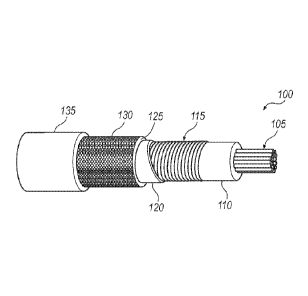
[0009] Figure 1 illustrates an exemplary wire assembly that may take many
different forms
and include multiple and/or alternate components and facilities. While an
exemplary wire
2
CA 02856532 2014-05-21
WO 2013/082140
PCT/US2012/066837
assembly is shown, the exemplary components illustrated are not intended to be
limiting.
Indeed, additional or alternative components and/or implementations may be
used.
[0010] Figure 1 illustrates different layers of an exemplary wire assembly
100. As illustrated,
the wire assembly 100 includes strength members 105, a first coating layer
110, a conductive
element 115, a second coating layer 120, an insulation layer 125, a shield
130, and a jacket
135.
[0011] The strength members 105 may be configured to structurally support to
the wire
assembly 100 yet allow some flexibility. In one exemplary approach, each
strength member
105 may include a strand or fiber of one or more of the following materials:
glass, aramid
fiber, metal, solid plastic, etc. The strength members 105 may be
alternatively formed from
one or more different materials or a combination of materials.
[0012] The first coating layer 110 may be disposed on the strength members
105. In one
possible approach, the first coating layer 110 may be formed from any material
that allows
the strength member 105 to maintain a desired amount of flexibility while
limiting movement
of moisture among the strength members 105. Some properties of the first
coating layer 110
may include low thermal conductivity, low chemical reactivity, electrical
insulation,
sufficient adhesion to the strength members 105, etc. Representative examples
of materials
used in the first coating layer 110 may include forms of latex or silicone.
[0013] The first coating layer 110 may be adhered to the strength members 105
in a way that
at least partially fills air gaps that would otherwise exist between the
strength members 105.
For example, the first coating layer 110 may sometimes exist in a fluid form
that can be cured
or otherwise hardened. During manufacture of the wire assembly 100, the
strength members
105 may be bundled and dipped into the fluid form of the first coating layer
110. When in
fluid form, the first coating layer 110 may have a viscosity that allows the
fluid material to
flow into and fill air gaps between strength members 105. The first coating
layer 110 may
solidify when cured or otherwise hardened. Moreover, the adhesive properties
of the first
coating layer 110 may allow the first coating layer 110 to remain adhered to
the strength
members 105 even after solidifying.
[0014] In addition to having the characteristics above, the first coating
layer 110 may have
other characteristics based upon the intended use of the wire assembly 100.
For instance, the
first coating layer 110 may be formed from a material that can adequately
protect the strength
members 105 from water if the wire assembly 100 will be subject to moisture
caused by
3
CA 02856532 2014-05-21
WO 2013/082140
PCT/US2012/066837
humidity. The first coating layer 110 may be formed from a material that can
seal the strength
members 105 from oil if the wire assembly 100 will likely be exposed to oil.
[0015] The conductive element 115 may be helically wound about the first
coating layer 110.
The conductive element 115 may be formed from any conductive material such as,
copper,
aluminum, tin, gold, or the like depending on the desired magnitude of
resistance, referred to
as a predetermined resistance below. The conductive material 115 may further
be formed
from a conductive material that can, e.g., be drawn into a wire or rolled into
a foil. For
instance, the conductive element 115 may include the foil where relatively low
resistance is
desired or the wire where relatively high resistance is desired. Various
physical properties of
the conductive element 115 may contribute to the resistance of the conductive
element 115.
For example, the length, cross-sectional area, thickness, gauge, and
resistivity of conductor
material used may each contribute to the resistance. Controlling one or more
of these
properties of the conductive element 115 may be used to adjust the resistance
of the
conductive element 115 to achieve the predetermined resistance.
[0016] The predetermined resistance may include a minimum desired value of
resistance
needed for proper operation of the wire assembly 100. By manufacturing the
conductive
element 115 to contain the predetermined resistance, the wire assembly 100 can
operate
despite omitting certain components such as resistors and over molds located
at terminal ends
of the wire assembly 100. The conductive element 115 may contribute most or
all of the
predetermined resistance to the wire assembly 100. Other components may also
contribute to
the predetermined resistance, as discussed in greater detail below.
[0017] Any number of characteristics of the conductive element 115 may be
manipulated to
manufacture the wire assembly 100 with the predetermined resistance. These
characteristics
may include the resistivity of the material used to form the conductive
element 115, the
length of the conductive element 115, and the cross-sectional area or
thickness of the
conductive element 115. In one possible implementation, the conductive element
115 may
include a wire helically wound about the first coating layer 110 to form a
coil wrap. The
length and size of the wire may be associated with the predetermined
resistance. That is, the
resistance of the wire may be directly proportional to the length of the wire
and inversely
proportional to the cross-sectional area or thickness of the wire. During
manufacture, the wire
may be drawn to have a substantially uniform cross-sectional area and length
associated with
the predetermined resistance and other constraints. Since the wire is wound
about the first
coating layer 110, the resistance of the coil wrap may be associated with a
specific number of
4
CA 02856532 2014-05-21
WO 2013/082140
PCT/US2012/066837
turns per inch, yard, or any other measure of distance, depending on the
circumference of the
first coating layer 110. Alternatively, the conductive element 115 may include
foil wound
about the first coating layer 110 to form a foil wrap. As with the coil wrap,
the length and
cross-sectional area or thickness of the foil may be associated with the
predetermined
resistance. Accordingly, the resistance of the foil wrap may be associated
with a specific
number of turns per unit of length depending on the circumference of the first
coating layer
110.
[0018] The second coating layer 120 may be disposed on the conductive element
115 and
first coating layer 110. The second coating layer 120 may be formed from the
same or a
different material than the first coating layer 110. Like the first coating
layer 110, the material
of the second coating layer 120 may allow for a minimum amount of flexibility
and may be
selected to accommodate the intended use of the wire assembly 100. For
instance, the second
coating layer 120 may be formed from a material that can prevent water
infiltration if
humidity or water exposure is expected of possible. A material that can seal
the conductive
element 115 from oil infiltration may be used if oil exposure is likely. The
second coating
layer 120 may be further formed from a material that can adhere to the
conductive element
115 and the first coating layer 110. The second coating layer 120 may have
additional
properties such as low thermal conductivity and low chemical reactivity.
Representative
examples of materials used for the second coating layer 120 may include forms
of silicone or
latex. In some situations both coating 110 and coating 120 may be formed from
the same
compound. In some implementations, the second coating layer 120 may be formed
from an
insulating material. The second coating layer 120 may be alternatively formed
from a
semiconductor material. Generally, semiconductor materials exhibit more
electrical
conductivity than an insulator but less than a conductor, such as the
conductive element 115.
Semiconductors may further exhibit resistivity. In this implementation where
the second
coating layer 120 is formed from a semiconductor material, the resistivity of
the second
coating layer 120 may further contribute to the predetermined resistance.
Accordingly, the
length of the conductive element 115 may be shorter or the cross-sectional
thickness of the
conductive element 115 may be larger if the second coating layer 120 includes
a
semiconductor material.
[0019] Air gaps near the strength members 105, the first coating layer 110,
the conductive
element 115, and the second coating layer 120 may cause moisture to wick
through the wire
assembly 100. One way to eliminate air gaps between the strength members 105
is discussed
CA 02856532 2014-05-21
WO 2013/082140
PCT/US2012/066837
above. One way to eliminate air gaps between at least a portion of the first
coating layer 110,
the conductive element 115, and the second coating layer 120, and thus seal
the conductive
element 115 from moisture, is to apply the second coating layer 120 to the
conductive
element 115 and first coating layer 110 via pressure extrusion. When applied
through
pressure extrusion, the second coating layer 120 fills air gaps that could
otherwise exist
between at least a portion of the first and second coating layers 110, 120 and
the conductive
element 115. The portion of the first and second coating layers 110, 120
sealed may be of any
length to prevent moisture from collecting in and wicking through the wire
assembly 100.
The length of the sealed portion may be measured by any unit of distance, such
as
millimeters, centimeters, inches, feet, meters, yards, etc., depending on the
overall length of
the wire assembly 100. Alternative methods of applying the second coating
layer 120 to the
conductive element 115 may also provide sufficient protection by, e.g.,
reducing a significant
number of air gaps or even eliminating the air gaps altogether.
[0020] The insulation layer 125 may include any material that may be disposed
on the second
coating layer 120 to provide further protection to the wire assembly 100 while
allowing the
wire assembly 100 to remain sufficiently flexible. The insulation layer 125
may be formed
from the same or a different material than the first coating layer 110 or the
second coating
layer 120. The insulation layer 125 may be applied to the second coating layer
120 via an
extrusion process. In some instances, such as low-voltage implementations, the
insulation
layer 125 may be the outermost layer of the wire assembly 100. Other
implementations,
however, may necessitate additional layers. For instance, in higher voltage
instances, for
noise prevention, or for shield 130ing purposes, additional layers, such as
the shield 130 and
the jacket 135, may be used.
[0021] The shield 130 may be configured to protect the conductive element 115
from
electrical interference as well as prevent the conductive element 115 from
transmitting
interfering signals. For example, the shield 130 may include a metal mesh or
braided wires
wrapped about the insulation layer 125. In operation, the shield 130 may be
configured to
disperse electromagnetic fields generated or received by the conductive
material.
[0022] The jacket 135 may be disposed on the shield 130 and allow for
sufficient flexibility
and insulation of the wire assembly 100. The jacket 135 may be formed from the
same or a
different material than the insulation layer 125, the first coating layer 110,
or the second
coating layer 120.
6
CA 02856532 2014-05-21
WO 2013/082140
PCT/US2012/066837
[0023] Figure 2 illustrates an example process 200 that may be used to
assemble the
components of the wire assembly 100. Any of the steps of the process 200 may
be performed
simultaneously or sequentially.
[0024] At block 205, the strength members 105 may be coated with the first
coating layer
110. One way to coat the strength members 105 is to bundle the strength
members 105 and
dip the bundled strength members 105 into a fluid form of the first coating
layer 110. Dipping
the strength members 105 into the liquid form of the first coating layer 110
may allow the
first coating layer 110 to substantially fill and eliminate air gaps between
the strength
members 105. This reduction of air gaps may effectively prevent moisture from
wicking
through the strength members 105. Coating the plurality of strength members
105 may
further include curing or otherwise hardening the first coating layer 110. The
first coating
layer 110 may be cured chemically or may simply harden over time. After the
first coating
layer 110 cures or hardens, the process 200 may continue at block 210.
[0025] At block 210, the conductive element 115 may be helically wound about
the first
coating layer 110. For instance, the conductive element 115 may be drawn into
a wire or
rolled into a foil and applied to the first coating layer 110 in a generally
spiral fashion to form
either a coil wrap or a foil wrap, respectively. The length or cross-sectional
thickness of the
conductive element 115 may be selected based upon a desired, predetermined
resistance of
the conductive element 115. The resistance of the conductive element 115 may
be designated
as a number of turns per unit of length, depending upon the circumference of
the first coating
layer 110.
[0026] At block 215, the second coating layer 120 may be applied to the
conductive element
115 and the first coating layer 110. The second coating element may be applied
via pressure
extrusion to reduce or otherwise fill air gaps that would otherwise exist on
or near the first
coating layer 110, the second coating layer 120, and the conductive element
115. Eliminating
air gaps may reduce or prevent moisture wicking through the wire assembly 100.
[0027] At block 220, the insulation layer 125 may be applied to the second
coating layer 120
via, e.g., extrusion. In one exemplary approach, the process 200 may continue
at block 225
after the insulation layer 125 is applied. In some instances, however, the
extrusion that occurs
at block 220 may further apply the shield 130, jacket 135, or both, to the
wire assembly 100.
Relative to the insulation layer 125, the shield 130 and jacket 135 may be
subsequently or
simultaneously applied to the wire assembly 100.
7
CA 02856532 2014-05-21
WO 2013/082140
PCT/US2012/066837
[0028] At block 225, the wire assembly 100 may be tested and packaged
depending on the
outcome of the testing. The process 200 may end after block 225.
CONCLUSION
[0029] With regard to the processes, systems, methods, heuristics, etc.
described herein, it
should be understood that, although the steps of such processes, etc. have
been described as
occurring according to a certain ordered sequence, such processes could be
practiced with the
described steps performed in an order other than the order described herein.
It further should
be understood that certain steps could be performed simultaneously, that other
steps could be
added, or that certain steps described herein could be omitted. In other
words, the
descriptions of processes herein are provided for the purpose of illustrating
certain
embodiments, and should in no way be construed so as to limit the claims.
[0030] Accordingly, it is to be understood that the above description is
intended to be
illustrative and not restrictive. Many embodiments and applications other than
the examples
provided would be apparent upon reading the above description. The scope
should be
determined, not with reference to the above description, but should instead be
determined
with reference to the appended claims, along with the full scope of
equivalents to which such
claims are entitled. It is anticipated and intended that future developments
will occur in the
technologies discussed herein, and that the disclosed systems and methods will
be
incorporated into such future embodiments. In sum, it should be understood
that the
application is capable of modification and variation.
[0031] All terms used in the claims are intended to be given their broadest
reasonable
constructions and their ordinary meanings as understood by those knowledgeable
in the
technologies described herein unless an explicit indication to the contrary in
made herein. In
particular, use of the singular articles such as "a," "the," "said," etc.
should be read to recite
one or more of the indicated elements unless a claim recites an explicit
limitation to the
contrary.
8