Note: Descriptions are shown in the official language in which they were submitted.
CA 02857015 2014-05-26
4
DESCRIPTION
OPTICAL MODULATOR
Technical field
[0001]
The present invention relates to an optical modulator that
is applicable to an optical communication system.
Background art
[0002]
In an optical fiber communication system, it is an
important problem to improve a receiving sensitivity to expand
a transmission distance. Recently, thanks to rapid progress
of a digital coherent technology by a combination of digital
signal processing (DSP) and a coherent transmission technology,
selections of modulation formats in optical communications have
largely been widened. Therefore, there have been made many
attempts to improve the receiving sensitivity by innovation of
the modulation format.
[0003]
Polarization-switched quadrature phase-shift keying
(PS-QPSK) may be exemplified as a representative high receiving
sensitivity modulation system. The PS modulation is
modulation for switching the momentary polarization between two
quadrature polarizations (X and Y) in response to data of 0 or
1, and thereby, an information amount of one bit/symbol can be
- 1 -
CA 02857015 2014-05-26
added as compared to a single polarization signal having the
same multi-valued degrees. The PS-QPSK is modulation of a total
of three bits/symbol by a combination of the QPSK of two
bits/symbol and the PS modulation.
[0004]
As to an optical modulation system utilizing the
polarization, a polarization division multiplexing (PDM)
system that uses two quadrature polarizations respectively as
independent channels is widely known. The PDM can double the
information amount as compared to the single polarization
signal (2 x 2 = 4 bits/symbol in case of PDM - QPSK). On the
other hand, the receiving sensitivity in the same symbol rate
is reduced to a half as compared to that in the single
polarization signal. Since the modulation is momentarily
performed by the single polarization in a case of the PS
modulation, the information amount can be increased without
deteriorating the receiving sensitivity.
[0005]
In fact, Non-Patent Literature 1 shows that a signal point
arrangement of PS-QPSK is an optimal arrangement in view of
receiving sensitivity in a four dimensional space having
respective components of X polarization in-phase (XI), X
polarization quadrature (XQ), Y polarization in-phase (YI) and
Y polarization quadrature (YQ) as a base. Further, also in
Non-Patent literature 2, long distance transmission of 13600km
using a PS-QPSK signal of 42.7Gbps is reported, which
experimentally indicates that the PS-QPSK can be sufficiently
- 2 -
CA 02857015 2014-05-26
applied also to the long distance transmission in the degree
of Pacific Ocean crossing.
[0006]
As to a method of generating the PS-QPSK signal, two kinds
of methods shown in Fig. 2 in Non-patent Literature 1 are well
known. That is, one is a method (conventional art 1) for
serially connecting a QPSK modulator and a polarization
modulator, and the other is a method (conventional art 2) in
which a PDM-QPSK modulator is used, and a particular correlation
is formed between signals of four lines driving the PDM-QPSK
modulator, whereby a half of signal points of the PS-QPSK is
thinned out to generate the PS-QPSK signal.
[0007]
Fig. 1 shows a configuration example of a modulator using
the conventional art 1. In this example, a QPSK modulation unit
191 is serially connected to a polarization modulation unit 192.
In Fig. 1, the QPSK modulation unit 191 has a general
configuration, that is, the configuration in which an optical
splitting circuit having an optical intensity splitting ratio
of 1:1 (0.5:0.5) and an optical coupling circuit having an
optical coupling ratio of 1:1 (0.5:0.5) are provided, and BPSK
modulation units 111 and 112 that perform binary phase
modulation (Binary-PSK: BPSK) are respectively arranged in the
respective arms in a Mach-Zehnder (MZ ) circuit configured of the
splitting and coupling circuits, and further, a phase shifter
121 is provided in the one-side arm for making a phase change
of 7/2. It is the most general to use an MZ circuit having
- 3 -
CA 02857015 2014-05-26
high-speed phase modulation units in both the arms (hereinafter,
simply "MZ modulation circuit") as the BPSK modulation unit.
The BPSK modulation units 111 and 112 and the polarization
modulation unit 192 are respectively driven by binary data
signals dl, d2, and d3.
[0008]
In this example, there will be considered a case where
operation polarization of the BPSK modulation units 111 and 112
is set to X polarization, and X polarization continuous light
of intensity 1 is input to a main input port 101. When an input
optical field to the main input port 101 expressed by Jones
vector of X, Y base (the 1st row corresponds to X polarization,
and the 2nd row corresponds to Y polarization) is indicated at
Ein, and an output optical filed from a main output port 102
is indicated at Eout, Eout can be expressed according to the
following equation.
[0009]
[Formula 1]
Eout= T2TiEin
= Vri r2 b1 + e -\,/ (1 - r1 ) (1 - r2) b2 0
0 a
= ( + j b2 0)
2 O a)
0)
T2 ¨
(1 ¨ p 0)
= (01)
- 4 -
CA 02857015 2014-05-26
...Eout -!-((11-1-
)(b12))
(Equation 1)
[0010]
Herein, TI and T2 respectively are Jones matrixes of X,
Y base expressing transmission characteristics of the QPSK
modulation unit 191 and the polarization modulation unit 192.
r1 is an optical intensity splitting ratio of the optical
splitting circuit 131 and r2 is an optical coupling ratio of
the optical coupling circuit 132, and in the present embodiment,
r1= r2 = 0.5. b1 and b2 are respectively modulation parameters
of the BPSK modulation units 111 and 112, and have either one
of +1 or -1 in a symbol point (center timing of a symbol on time
axis). p is a modulation parameter of the polarization
modulation unit 192, and has either one of 1 or 0 in a symbol
point. a is transmittance of the QPSK modulation unit 191 to
Y polarization, and since input light to the modulation unit
is X polarization, a value of a does not affect the output light.
[0011]
It should be noted that in the present specification, the
optical splitting unit, the optical coupling unit, the BPSK
modulation unit, other circuit elements (including a
polarization rotating unit and a polarization coupling unit
which will be described later), and optical waveguides for
connecting them are all assumed to be in an ideal state where
the excessive loss is zero, for model simplification. All the
circuit elements except the polarization modulation unit and
the polarization rotating unit are assumed to be in an ideal
- 5 -
CA 02857015 2014-05-26
state where the polarization rotation is not generated (that
is, in a state where off-diagonal elements of Jones matrix are
zero).
[0012]
Fig. 2A, Fig. 2B and Fig. 20 show two kinds of diagrams
indicating a relation between d1 to d3 and Ec,õt in the modulator
configuration shown in Fig. 1. Fig. 2A and Fig. 2B are
respectively complex signal diagrams each having an X
polarization component and a Y polarization component. The
respective lateral axes indicate optical electrical field
amplitudes Exi and Eyy of I phase, and the respective vertical
axes indicate optical electrical field amplitudes ExQ and EyQ
of Q phase . Next, for distinction from Fig. 2C to be described,
such a diagram is hereinafter called "IQ diagram". Fig. 20
is a diagram where a lateral axis indicates phase (1)x. of an X'
polarization component and a vertical axis indicates phase (I)y,
of a Y' polarization component. As shown in Fig. 10, however,
X' polarization axis and X polarization axis, and Y'
polarization axis and Y polarization axis are respectively
defined to be shifted by 45 degrees with each other. In addition,
an indication range (entire width) of each of the lateral axis
and the vertical axis is set to 2n. This diagram is often used
for expressing PS-QPSK signal point arrangement (for example,
Non-Patent Literature 3), and this diagram is hereinafter
called "XY diagram" for distinction from Fig. 2A and Fig. 2B.
[0013]
- 6 -
CA 02857015 2014-05-26
A relation between Jones vector Eõt of the output optical
light, and vertical axis values and lateral axis values of the
respective diagrams (ExT, En, Eyi, En, (I)x, and (I)y.) will be put
in order as follows.
[0014]
[Formula 2]
=
(Ex/ jEx(2 = ( 1 1) (Ax' exp(j Ox, ))
Eout
Ey, + jEy(2 )
¨1 1 Ay, exp(j y')
Ax = (Ex/ ¨ E1 )2(Ex(2 EYQ )2
AY = "\/(EX1 + 41)2 + (E" + EyQ)2
(Equation 2)
a r g { Exi ¨ Ey, + xcl ¨ EyQ )}
(I)y = a rg {Ex/ + Ey, + xQ EyQ )}
[0015]
It should be noted that in the modulation system which
does not include intensity modulation, such as PS-QPSK,
PDM-QPSK or the like, Ax, and Ay, always have constant values.
Therefore, (1)x, and (I)y are sufficient as parameters for expressing
the signal point arrangement, and the arrangement of all the
signal points can be expressed by a single diagram when the XY
diagram is used.
[0016]
According to Equation 1 and Equation 2, a relation between
vertical axis values and lateral axis values of the respective
diagrams and modulation parameters of the respective modulation
units is as follows.
- 7 -
CA 02857015 2014-05-26
[0017]
[Formula 3]
,
Exi = poi
,__
ExQ := -2 pp2
1
Eyi = -2 (1 p)
(Equation 3)
EyQ = -2 (1 ¨ p) b2
(1)]<1 = arg1(2P-1)bi+j(2p-1)b21
(1)yl = argIbi+j1021
[0018]
[d1d2d3] in Fig. 2A, Fig. 2B, and Fig. 2C indicate mapping
of drive binary data to the respective signal points. A data
bit value is associated with a value of a modulation parameter
in each BPSK modulation unit in a symbol point in a one-to-one
relation. Herein, as to the BPSK modulators 111 and 112 (n =
1, 2) in Fig. 1, when cin = 0, bn = +1 (phase 0), and when dn =
1, b = -1 (phase 7). In addition, as to the polarization
modulation unit 192 in Fig. 1, when d3 = 0, p = 1, and when d3
= 1, p = 0. According to the above corresponding relation and
the Equation 3, the mapping shown in each of Fig. 2A, Fig. 2B
and Fig. 2C can be obtained.
[0019]
As shown in the IQ amplitude diagram in each of Fig. 2A
and Fig. 2B, when d3 = 0, signal intensity of Y polarization
is zero, when d3= 1, signal intensity of X polarization is zero,
and a signal state in a polarization side of intensity non-zero
takes four values equivalent to the QPSK signal arrangement
corresponding to d] and d2.
- 8 -
CA 02857015 2014-05-26
[0020]
As shown in Fig. 2C, when the XY diagram is used, signal
points of 23= 8 points of PS-QPSK which is three bits / symbol
modulation can be all expressed at a time. When an output signal
is X polarization (d3 = 0), a phase difference between X'
component and Y' component is zero. Therefore, the
corresponding point is on a straight line of inclination 1
passing through the origin. When the output signal is Y
polarization (d3= 1), the phase difference between X' component
and Y' component is M. Therefore, the corresponding point is
on a straight line where the section is it or -7E, and the
inclination is 1.
[0021]-[0025]
Fig. 3 shows a modulator configuration example using the
conventional art 2. In this example, a PDM-QPSK modulator 300
is used. The PS-QPSK 300 uses a general configuration, that
is, the configuration that QPSK modulation units 391 and 392
having the same configuration as that of the conventional art
1 are connected to the respective outputs of an optical
splitting unit 330 having a splitting ratio of 1 : 1, the output
of the QPSK modulation unit 391 is connected directly to a
polarization coupling unit 352, and the output of the QPSK
modulation unit 392 is connected through a 90-degree
polarization rotating unit 351 to the polarization coupling
unit 352. BPSK modulation units 311 to 314 are respectively
driven by binary data signals d1 to d4. Among them, d1 to d3
use independent data signals, and d4 is generated to be [Formula
- 9 -
CA 0285.7015 2014-05-26
4: d4 = (di CI d2) e d3] ( [Formula 5: "0"] expresses XOR
calculation) .
[0026]
Hereinafter, there will be considered a case where
operation polarization of the BPSK modulation units 311 and 314
is indicated at X' for descriptive purposes, and X' polarization
continuous light of intensity 1 is input to a main input port
301. When Jones vector of X' , Y' base (the 1st row corresponds
to X' polarization and the 2nd row corresponds to Y'
polarization) of output light from a main output port 302 is
indicated at Eat, and Jones vector of X, Y base (the 1st row
corresponds to X polarization and the 2nd row corresponds to
Y polarization) is indicated at Eout, the following relation is
established.
[0027]
[Formula 6]
1
Emit = {Si Ti'¨ + S2 R T2
v2 0
T1 = ( + j b2 0
2 0 al)
T2 -1 b3 b4 )
2 0 a2
R' (0 -1)
0)
(1 0)
0)
- 10 -
CA 02857015 2014-05-26
s2 (0 0)
0 1)
=
: (13
.E,õ ' - 7,3 jx.,Lb2
1 + J)
-
2V2 1./
t 4
E. 1 ,'1 1) b3 j (b2 b4.)
Eout' =- (Equation 4)
t -12--1 1 4 b3 j (--b2 b4))
[0028]-[0030]
Here, Ti' and T2' are respectively Jones matrixes of X',
Y' base expressing transmission characteristics of the QPSK
modulation units 391 and 392, R' is Jones matrix of X', Y' base
expressing transmission characteristics of the 90-degree
polarization rotating unit 351, S1' and S2' are respectively
Jones matrixes of X', Y' base expressing transmission
characteristics of the polarization coupling unit 352 to inputs
from a port 1 (side of the QPSK modulation units 391) and a port
2 (side of the QPSK modulation unit 392). A coefficient
[Formula7:-F]of a right side in the first line expresses
v2
a branch by the optical splitting unit 330. bl to b4 are
respectively modulation parameters of the BPSK modulation units
311 to 314, and take either one of +1 or -1 in a symbol point
(center timing of a symbol on time axis). al and a2 are
respectively transmittances of the QPSK modulation units 391
and 392 to Y' polarization, and since input light to the
modulation unit is X' polarization, values of al and a2 do not
affect the output light.
[0031]
- 11 -
CA 02857015 2014-05-26
=
According to Equation 2 and Equation 4, the following
relation is established in the present example.
[0032]
[Formula 8]
Exi = -4 (b1 + b3)
1
ExQ ( b2 b4)
Eyi = - ( -b1 b3)
(Equation 5)
4
1
EyQ -1-)2 + b4)
4
(1)x = arg{bi + j132
(1)y = arg{b3 + jb4}
[0033]
Fig. 4B shows an XY diagram expressing a relation between
d1 to d4 and E,,,t in the modulator configuration shown in Fig.
3. [d1
d2 d3 d4] in the figure indicates mapping of drive binary
data to each signal point. A data bit value is associated with
a value of a modulation parameter in each BPSK modulation unit
in a symbol point in a one-to-one relation. Herein, when dr,
=0, b=+1 (phase 0) , and when dn= I, bn= -1 (phase TO . According
to the above corresponding relation and Equation 5, the mapping
shown in Fig. 4B can be obtained.
[0034]
For facilitating understanding of the operation principle
in the present example, Fig. 4A firstly shows a signal point
arrangement in a case where all of d1 to d4 are provided as
independent data, that is, in a case of a regular PDM-QPSK drive.
It is found out that signal points of 24 = 16 points of PDM-QPSK
which is four bits /symbol modulation are arranged in a lattice
- 12 -
CA 02857015 2014-05-26
shape of 4 x 4. [d1 d2] corresponds to a lateral axis and [d3
d4] corresponds to a vertical axis.
[0035]-[0037]
Next, by referring to Fig. 4B, it is found out that by
associating d4 with d1 to d3 as [Formula 9: d4= (d1 d2) E0 d3]
according to the drive method in this example, a half of the
signal points are thinned out to produce a signal point
arrangement of PS-QPSK as similar to that of Fig. 2C.
Citation List
Non-Patent Literature
[0038]
NPL 1: M. Karlsson and E. Agrell, "Which is the most
power-efficient modulation format in optical links?, " Opt.
Exp., vol. 17, no. pp. 10814-10819, 2009.
NPL 2: C. Behrens, D. Lavery, D. S. Millar, S. Makovejs,
B. C. Thomsen, R. I. Killey, S. J. Savory and P. Bayvel,
"Ultra-long-haul transmission of 7 x 42.9Gbit/s PS-QPSK and
PM-BPSK, " Proc. ECOC2011, Mo. 2. B. 2, 2011.
NPL 3: J. K. Fischer, L. Molle, M. Nolle, D. - D. Gross,
C. Schubert, "Experimental Investigation of 28-GBd
Polarization-Switched Quadrature Phase-Shift keying Signals, "
Proc. ECOC2011, Mo. 2. B. 1, 2011.
NPL 4: N. Kikuchi, "Intersymbol Interference (ISI)
Suppression Technique for Optical Binary and Multilevel Signal
Generation, " J. Lightwave Technol., Vol. 25, No. 25, No. 8,
pp. 2060-2068, 2007.
- 13 -
CA 02857015 2014-05-26
NPL 5: K. Jinguj 1, and M. Kawachi, "Synthesis of Coherent
Two-Port Lattice-Form Optical Delay-Line Circuit, "J.
Lightwave Technol. , Vol. 13, No. 1, pp. 73-82, 1995.
NPL 6: K. Jinguji, N. Takato, A. Sugita, and M. Kawachi,
"Mach-Zehnder interferometer type optical waveguide coupler
with wavelength-flattened coupling ratio, "Electron. Lett.,
Vol. 26, No. 17, pp. 1326-1327, 1990.
Summary of Invention
Technical Problem
[0039]
However, the above conventional arts 1 and 2 have a common
problem that intrinsic optical loss is generated due to the
modulator configuration. Note that "intrinsic optical loss
due to the modulator configuration" (hereinafter, simply
"intrinsic loss") herein means an optical loss unavoidably
generated in generating processes of optical signals also under
an ideal condition that propagation loss of an optical waveguide,
loss by process errors or the like are zero. Output optical
intensity in a symbol point in the conventional art 1 or 2 in
a case where the input optical intensity is set to 1 is equivalent
to lEouti2 in Equation 1 and Equation 4, but it is found out that
in any case, I E0ut12 = 1/2 all the time, and intrinsic loss of
3dB is generated.
[0040]
In addition, the conventional art 1 has a problem that
an additional loss is further generated due to the configuration
- 14 -
CA 02857015 2015-12-23
95546-8T
of the polarization modulation unit. For
example, in
Non-Patent Literature 3, output light of the QPSK modulation
unit is split into two paths, and an on-off modulator is provided
in each path to always block either one of the two split signals,
which is output through a polarization beam combiner in such
a manner as to output polarization that differs depending on
the passed optical path. However, in this configuration, an
excessive loss of 3dB is generated in the polarization
modulation unit (on-off modulation unit).
[0041]
In addition, in the conventional art 2, an electronic
circuit including an XOR gate for generating d4 is necessary
and further, binary data drive systems of four lines and four
BPSK modulation units are required for modulation of three
bits/symbol. Therefore, there is a problem that the device
becomes complicated. (In general, the number of the binary data
drive systems and the number of the BPSK modulation units are
respectively N.)
[0042]
The present invention is made in view of this problem,
and an object of the present invention is to provide a PS-QPSK
optical modulator in which intrinsic optical loss is not
generated and a configuration is simple.
Solution to Problem
[0043]
For solving the above problem, an optical modulator in
the present invention includes an input optical splitting unit
- 15 -
CA 02857015 2015-12-23
95546-8T
for bifurcating input light from a main input port, a final
optical coupling unit for coupling optical signals of two lines
in a polarization state orthogonal to each other to output to
a main output port, an intermediate optical coupling unit
provided in an intermediate position between the input optical
splitting unit and the final optical coupling unit, the
intermediate optical coupling unit including at least two input
ports and at least two output ports, first and second optical
paths for connecting the input optical splitting unit and the
intermediate optical coupling unit, optical path lengths of the
first and second optical paths are approximately equal to each
other, third and fourth optical paths for connecting the
intermediate optical coupling unit and the final optical
coupling unit, optical path lengths of third and fourth optical
paths are approximately equal to each other, and three binary
phase modulation unit arranged one by one in each of the three
optical paths of the first, second, third and fourth optical
paths.
[0044]
In addition, an optical modulator in the present invention
is characterized in that each of the binary phase modulation
unit is a Mach-Zehnder modulation circuit.
[0045]
In addition, an optical modulator in the present invention
includes a phase adjusting unit for adjusting a relative optical
phase between the first and second optical paths.
- 16 -
CA 02857015 2015-12-23
95546-8T
[0046]
In addition, an optical modulator in the present invention
includes an optical intensity adjusting unit provided in a
single optical path, in which the binary phase modulation unit
is not arranged, among the first, second, third and fourth
optical paths.
Advantageous Effects of Invention
[0047]
According to the present invention, there is provided a
PS-QPSK optical modulator in which intrinsic optical loss is
not generated and the configuration is simple.
Brief Description of Drawings
[0048]
[Fig. 1] Fig. 1 is a diagram illustrating a circuit
configuration of a PS-QPSK modulator according to a first
conventional art;
[Fig. 2A] Fig. 2A is an output signal diagram of the PS-QPSK
modulator according to the first conventional art;
[Fig. 2B] Fig. 2B is an output signal diagram of the PS-QPSK
modulator according to the first conventional art;
[Fig. 2C] Fig. 2C is an output signal diagram of the PS-QPSK
modulator according to the first conventional art;
- 17 -
CA 02857015 2014-05-26
[Fig. 3] Fig. 3 is a diagram illustrating a circuit
configuration of a PS-QPSK modulator according to a second
conventional art;
[Fig. 4A] Fig. 4A is an output signal diagram of the PS-QPSK
modulator according to the second conventional art;
[Fig. 4B] Fig. 4B is an output signal diagram of the PS-QPSK
modulator according to the second conventional art;
[Fig. 5] Fig. 5 is a diagram illustrating a circuit
configuration of a PS-QPSK modulator according to a first
embodiment in the present invention;
[Fig. 6A] Fig. 6A is an output signal diagram illustrating
an optical signal state in an inside of the PS-QPSK modulator
according to the first embodiment in the present invention;
[Fig. 6B] Fig. 6B is an output signal diagram illustrating
an optical signal state in an inside of the PS-QPSK modulator
according to the first embodiment in the present invention;
[Fig. 6C] Fig. 6C is an output signal diagram illustrating
an optical signal state in an inside of the PS-QPSK modulator
according to the first embodiment in the present invention;
[Fig. 7A] Fig. 7A is a final output signal diagram of the
PS-QPSK modulator according to the first embodiment in the
present invention;
[Fig. 7B] Fig. 7B is a final output signal diagram of the
PS-QPSK modulator according to the first embodiment in the
present invention;
- 18 -
CA 02857015 2014-05-26
[Fig. 7C] Fig. 7C is a final output signal diagram of the
PS-QPSK modulator according to the first embodiment in the
present invention;
[Fig. 8] Fig. 8 is a diagram illustrating a circuit
configuration of a PS-QPSK modulator according to a second
embodiment in the present invention;
[Fig. 9A] Fig. 9A is a final output signal diagram of the
PS-QPSK modulator according to the second embodiment in the
present invention;
[Fig. 9B] Fig. 9B is a final output signal diagram of the
PS-QPSK modulator according to the second embodiment in the
present invention;
[Fig. 9C] Fig. 9C is a final output signal diagram of the
PS-QPSK modulator according to the second embodiment in the
present invention; and
[Fig. 10] Fig. 10 is a diagram illustrating a definition
of polarization axes in the present specification.
Description of Embodiments
[0049]
The present invention relates to a circuit configuration
of a modulator. Since the effect does not depend on a material
forming the modulator, the material is not particularly
specified in embodiments as shown below. An example of the
material forming the modulator may include a multi-elemental
oxide crystal such as LiNb03 (LN), KTa1_xNbx03, or Ki_yLiyTai_xNb.03,
having a Pockels effect which is one kind of an electro-optic
- 19 -
CA 02857015 2014-05-26
(E0) effect, a GaAs or InP compound semiconductor in which
modulation of a refractive index or an absorption coefficient
by an electro-absorption (EA) effect or by a quantum confined
stark effect (QCSE) is possible, or a polymer having an EO effect,
such as chromophore. Further, for producing the modulator
circuit having a complicated configuration in a low loss, as
shown in Non-Patent Literature 1, a junction type configuration
by different kinds of substrates composed of the above material
substrate and silica planar lightwave circuits (PLCs) may be
used. Further, a bulk type optical element may be used as the
polarization rotating unit or the polarization coupling unit.
[0050]
Hereinafter, in the embodiment, the configuration of a
multilevel modulator by a combination of a plurality of BPSK
modulation units is shown. It is the most general to use an MZ
modulation circuit as the BPSK modulation unit. AS in detail
discussed in Non-Patent Literature 4, there is an advantage that,
when the MZ modulation circuit is driven in a push-pull manner
by a voltage amplitude that causes an arm-to-arm phase
difference +7 to -7, pulsation of optical output due to drive
electrical signal noises can be controlled to the minimum to
suppress interference between symbols. However, since the
effect of the present invention does not depend on a specific
configuration of the BPSK modulation unit, for example, a
straight phase modulator or the like may be used.
[0051]
- 20 -
CA 02857015 2014-05-26
It should be noted that, unless particularly mentioned,
optical path lengths of both the arms in the NZ circuit are all
equal. In fact, a deviation of the optical path length is
generated by a process error, a DC drifter or the like, but such
a deviation is generally compensated for by adjustment of a
phase shifter. Since the compensation amount variously
differs depending on materials, manufacturing conditions, use
environments of the modulator or the like, it cannot be uniquely
determined. Therefore, a value of a phase shift amount in the
phase shifter in the following embodiment will not contain a
phase shift amount for the optical path length compensation.
Hereinafter, in the embodiment, the phase shift is arranged only
in one arm of the NZ circuit in order to simplify the explanation
by equations, but since a phase difference between arms is an
essential parameter in the NZ circuit, in a case where the phase
shifter is arranged in the other arm or in both the arms, it
is obvious that the same effect can be obtained. The effect
of the present invention does not depend on the selection of
the arm (one arm, the other arm and both the arms) in which the
phase shifter is arranged.
[0052]
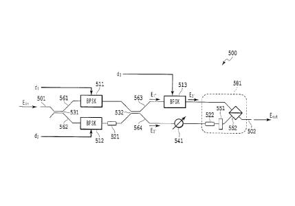
(First Embodiment)
Fig. 5 shows the configuration of a PS-QPSK modulator
according to a first embodiment in the present invention. The
PS-QPSK modulator includes a main input port 501, an input
optical splitting unit 531, an intermediate optical coupling
unit 532, a final optical coupling unit 581, optical paths 561
- 21 -
CA 02857015 2014-05-26
and 562 connecting the input optical splitting unit and the
intermediate optical coupling unit, optical paths 563 and 564
connecting the intermediate optical coupling unit and the final
optical coupling unit, BPSK modulation units 511, 512 and 513
arranged in the optical paths 561, 562 and 563 respectively,
a phase adjusting unit 521 for adjusting a relative phase
between the optical paths 561 and 562 to 7/2, an optical
intensity adjusting unit 541 arranged in the optical path 564,
and a main output port 502. An optical path length of the
optical path 561 is approximately equal to that of the optical
path 562, and an optical path length of the optical path 563
is also approximately equal to that of the optical path 564.
("the optical path lengths are approximately equal" herein
means that a group delay time difference between optical paths
is sufficiently smaller than the inverse of the modulation
symbol rate, that is, one symbol time.) The final optical
coupling unit 581 includes a phase adjusting unit 522 for
adjusting a relative phase between the optical paths 563 and
564 to zero, a polarization rotating unit 551 for rotating a
polarization of an optical signal of the optical path 564 by
90 degrees, and a polarization coupling unit 552. In addition,
since the excessive loss of the BPSK modulation unit is assumed
to be OdB in the present specification as described above, the
optical intensity adjusting unit 541 is also assumed to be set
to the loss of OdB. In fact, the loss of the optical intensity
adjusting unit 541 is set to a value equal to the excessive loss
of the BPSK modulation unit 513.
- 22 -
CA 02857015 2014-05-26
[0053]
The QPSK modulator formed of the input optical splitting
unit 531, the BPSK modulation units 511 and 512, the phase
adjusting unit 521, and the intermediate optical coupling unit
532 configures a QPSK modulation unit approximately equivalent
to that used in the above conventional arts 1 and 2, but differs
in a point where the optical splitting unit 531 and the coupling
unit 532 are a directional coupler of two inputs and two outputs
having an optical intensity coupling ratio of 1 : 1 (0.5 : 0.5) .
[0054]
As well known, transmission characteristics of the
directional coupler can be expressed according to the following
equation (refer to Non-Patent Literature 5 and the like) .
[0055]
[Formula 10]
Eout,c
r = E j ¨ r = E 13
E out , D = -j./1¨r = E + VT" = E in jj
(Equation 6)
[0056]
Note that Ein,A, and Ein,B are respectively input optical
fields from input ports A and B, and Eout,c and Eout,D are
respectively output optical fields from output ports C and D
(any of them is expressed by a complex number), and r is an
optical intensity coupling ratio.
[0057]
Hereinafter, operation polarization of the BPSK
modulation units 511 to 513 is indicated at X', and X'
polarization continuous light of intensity 1 is input to the
- 23 -
CA 02857015 2014-05-26
main input port 501. When the transmission characteristic,
which is expressed using Jones matrix of X', Y' base, from the
main input port to the output port in the side of the optical
path 561 in the intermediate optical coupling unit is indicated
at TI', and the transmission characteristic, which is expressed
using Jones matrix of X', Y' base, from the main input port to
the output port in the side of the optical path 562 in the
intermediate optical coupling unit is indicated at T2', TI' and
T2' can be expressed as follows.
[0058]
[Formula 11]
1
01( bi ¨j b2 0
\\
) = )
Ti , = v2 -v2 v2 v2
0 ad 2 0 al)
1 1 i b ---j
T2' - (-jh Vf'1.\/ 4- ff) 2 ad ) , 1. ( b2 - ibi a2))
0
(Equation 7)
0 2 0
[0059]
Herein, bl and b2 are respectively modulation parameters
of the BPSK modulation units 511 and 512, and take either one
of +1 or -1 in a symbol point (center timing of a symbol on time
axis). al and a2 are transmission rates to Y' polarization
respectively. Since the input light to the modulation unit is
X' polarization, values of al and a2 do not affect the output
light.
[0060]
When Jones vector of X', Y' base in the signal light in
the output port in the side of the optical path 563 in the
intermediate optical coupling unit is indicated at Ei', when
- 24 -
CA 02857015 2014-05-26
Jones vector of X', Y' base in the signal light in the output
port in the side of the optical path 564 is indicated at E2',and
when Jones vector of X', Y' base in the signal light immediately
after the BPSK modulation unit 513 is indicated at E3', E11,
E2 and E3' are as follows according to Equation 7.
[0061]
[Formula 12]
1 (b1¨ j b2)
El' = T141)
ql) 2
E2' = T2!() 1 ( b2 ¨0 bi)
(Equation 8)
(b3 , = b3(b1 ¨ j b2))
E3' =
0 0) 0
[0062]
Herein, b3 is a modulation parameter of the BPSK modulat ion
unit 513, and takes either one of +1 or -1 in a symbol point
(center timing of a symbol on time axis). a3 is a transmission
rate to Y' polarization of the BPSK modulation unit 513. Since
the input light to the modulation unit is X' polarization, a
value of a3 does not affect the output light. Comparing El'and
E2', plus and minus of a relative phase of bl term and b2 term
are replaced, and it is found out that these signal lights have
a relation of a positive phase signal and a reverse phase signal
with each other.
[0063]
When Jones vector of X', Y' base of the output light from
the main output port 502 is indicated at Emit' and when Jones
- 25 -
CA 02857015 2014-05-26
vector of X, Y base of the output light from the main output
port 502 is indicated at Eout, the following relation is
established.
[0064]
[Formula 13]
5õt' =S1tE3T + S2' R' eilt21
(1) = 0
( ¨1)
0 )
S1
= (1 0)
S2 , (0 0)
0 1)
...Eaut, = (b3 (b1 j b2))
2 b2
( 1 1) E b3 + b2 + j(¨bi ¨ b2 b3 )
Eout----Trz 1) out ¨212- 63 +b2 +j (-61 +b2 63))
(Equation 9)
[0065]
Herein, (I) is a phase shift amount of the phase adjusting
unit 522, and (j) = 0 in this example. R' is a transmission
characteristic of the 90-degree polarization rotating unit 551.
Each of S1' and S21 is Jones matrix of X', Y' base expressing
a transmission characteristic of the polarization coupling unit
552 to each of optical signals from the side of the optical path
563 and from the side of the optical path 564. In this example,
the polarization coupling unit 552 is a polarization beam
combiner of polarization axes X' and Y' .
- 26 -
CA 02857015 2014-05-26
[0066]
The following relation is established according to
Equation 2 and Equation 9 in this example.
[0067]
[Formula 14]
2v
ExT--(101b3+ b9)
2
1
ExQ (-b1 b2b3)
2v2
1
-Eyi = b1b3 + b2)
2v2
1
EYQ
+ b2b3)
(Equation 10)
-72 2
(1)x arg{b3 (bi-jb2}
(I)y = arg{b2-ib1}
[0068]
Fig. 6A, Fig. 6B, and Fig. 6C show IQ diagrams of X'
polarization indicating a relation between d1 to d3 in the
modulator configuration shown in Fig. 5, and El', E2' and
E3'shown in Equation 8. Fig. 6A is a diagram of El'. Fig. 6B
is a diagram of E2'. Fig. 6C is a diagram of E3'. [d1 d2
d3] in
the figure indicates mapping of drive binary data to each signal
point. A data bit value is associated with a value of a
modulation parameter in each BPSK modulation unit in a symbol
point in a one-to-one relation. Herein, when d. = 0, b. = +1
(phase 0), and when d. ¨ 1, b = -1 (phase n). When d3 = 0, p
= I, and when d3 = 1, p= 0. According to the above corresponding
relation and Equation 8, the mapping shown in each of Fig. 6A,
Fig. 6B and Fig. 6C can be obtained. It should be noted that
since El' and E2' do not depend on b3, data of the third bit in
Fig. 6A and Fig. 6B is set to x (any value).
- 27 -
CA 02857015 2014-05-26
[0069]
Comparing Fig. 6A and Fig. 68, it is found out that graphics
drawn by signal points are the same squares, but differ in data
mapping, and are in reverse direction with each other at tracing
along the signal points in the order of [0 0 x] , [0 1 x], [1
1 x] and [1 0 x] . That is, El.' and 82 have a relation of a normal
phase signal and a reverse phase signal. In addition, as shown
in Fig. 6C, it is found out that 83' becomes a QPSK signal in
which two kinds of data overlap in each signal point.
[0070]
Fig. 7A, Fig. 7B, and Fig. 7C show IQ diagrams and an XY
diagram indicating a relation between d1 to d3 in the modulator
configuration shown in Fig. 5 and Eout shown in Equation 9. Fig.
7A is an IQ diagram in regard to X polarization of Eout, Fig.
7B is an IQ diagram in regard to Y polarization of Eout, and Fig.
7C is an XY diagram of Eout. The mapping shown in each of Fig.
7A, Fig. 7B and Fig. 70 can be obtained according to the
corresponding relation of dn and bn, and Equation 10.
[0071]
As shown in Fig. 7C, it is found out that as similar to
the output signal in the conventional art shown in Fig. 2C or
Fig. 4B also in this example, the XY diagram composed of eight
signal points can be obtained and the PS-QPSK signal can be
obtained.
[0072]
A corresponding relation between Fig. 7C and Fig. 68, and
Fig. 6C can be explained as follows. As shown in Fig. 5, 82
- 28 -
CA 02857015 2014-05-26
is incident to the polarization coupling unit 552 as X'
polarization as it is, and E3' is polarization-rotated by 90
degrees to be incident to the polarization coupling unit 552
as Y' polarization. Therefore, A lateral axis in Fig. 7C
corresponds to a phase of E3' shown in Fig. 6C, and a vertical
axis in Fig. 7C corresponds to a phase of E2' shown in Fig. 6B.
A point [d1 d2 x] in Fig. 6B corresponds to any of four vertical
axis levels (-0.757, -0.257, +0.257, +0.757), and two points
corresponding to the vertical axis level correspond to [d1 d2
0] and [d1 d211 in Fig. 6C. For example, [1 0 x] in Fig. 6B
corresponds to +0.25n in the vertical axis level in Fig. 7C,
and two points corresponding to [1 0 0] and [1 0 1] appear in
the same vertical axis level.
[0073]-[0075]
Incidentally, the distance from the original point to
each signal point in the IQ diagrams in Fig. 7A and Fig. 7B is
[Formula 15: VT] times larger than that in the IQ diagrams in
Fig. 2A and 2B. This means that the output optical intensity
that is twice that of the conventional art can be obtained in
the present embodiment relative to the same input optical
intensity. As described before, in the conventional arts 1 and
2 (Equations 1 and 4) , Eoutl 2 = 1/2, and in the present embodiment
(Equation 9), lEcnitl 2 = 1. That is, the intrinsic loss 3dB is
generated in the conventional art, and the intrinsic loss is
OdB in the present embodiment.
[0076]
- 29 -
CA 02857015 2014-05-26
As explained above, the PS-QPSK signal can be generated
without generation of the intrinsic loss by a simple
configuration composed of the binary data drive systems of three
lines and the three BPSK modulation units.
[0077]
It is already apparent by Equation 9 that the intrinsic
loss is OdB in the present embodiment, but the principle is
explained in a qualitative and intuitive manner as follows. In
the conventional art, only either one of the signals
corresponding to Fig. 6A and Fig. 6B, that is, a normal phase
signal and a reverse phase signal is used for combination of
final output signals, and the other is discarded as radiated
light in the optical coupling unit as shown in Fig. 1 and Fig.
3. This causes the intrinsic loss of 3dB. There is generally
used the configuration of using the reverse phase signal (or
normal phase signal) as monitor signal light without being
discarded as the radiated light, but since the monitor signal
light does not contribute to the output signal light also in
this case, the intrinsic loss to the main output signal is the
same as in the case of discarding the reverse phase signal (or
normal phase signal) as the radiated light. In contrast, in
the present invention, it is possible to make the intrinsic loss
OdB with a new concept that one of the normal phase signal and
the reverse phase signal is further modulated and both thereof
are combined by quadrature polarization to obtain a final output
signal.
[0078]
- 30 -
CA 02857015 2014-05-26
In all the embodiments of the present invention including
the present embodiment, a multi-mode interference (MMI) coupler
or a wavelength insensitive coupler (WINC) shown in Non-Patent
Literature 6 in place of the directional coupler may be used
as the intermediate optical coupling unit of two inputs and two
outputs. The transmission function of these couplers differs
from Equation 6, but even if any coupler of two inputs and two
outputs is used, optical signals from the output port have a
relation of a normal phase signal and a reverse phase signal
with each other. This relation can be derived from reciprocity
of an optical coupler and the energy conservation law (exactly,
in some cases a signal diagram is disturbed by an inner loss
of a coupler, but there is no problem if a coupler having a
sufficiently small inner loss is used). Further, as the input
optical splitting unit, the output coupler of two inputs and
two outputs may be used as in the case of this example, or a
Y-branch coupler may be used. However,
since the phase
characteristic of a coupler differs depending on a kind of the
coupler, it is necessary to change the phase shift amount of
the phase shifter 521 from the above value in accordance with
the kind of the coupler.
[0079]
In the final optical coupling unit 581, the arrangement
of the polarization rotating unit 551 is provided not only to
the side of the optical path 564 as in the case of this example,
but also may be provided to the side of the optical path 563
to use a polarization coupling unit in accordance therewith.
- 31 -
CA 02857015 2014-05-26
In general, it is only required that polarization states in the
side of the optical path 563 and in the side of the optical path
564 are orthogonal to each other, and for example, a 0-degree
polarization rotating unit is provided in the side of the
optical path 563 and a 90-0-degree polarization rotating unit
may be provided in the side of the optical path 564, and
polarization coupling units in which the polarization axis is
fitted may be used to these output polarizations.
[0080]
In addition, in the optical coupling unit 581, the phase
adjusting unit 522 for adjusting a relative phase between
optical signals in the side of the optical path 563 and in the
side of the optical path 564 is provided and the phase shift
amount (I) is set to 0, but in fact, in many cases this phase
adjusting unit 522 may be eliminated. Because the relative
phase between the optical signals in the side of the optical
path 563 and in the side of the optical path 564 does not affect
the polarization orthogonality in the present configuration.
It is assumed that the phase adjusting unit 522 is eliminated
and a relative phase (1)0 between a third and second optical
signals is not controlled. (1)0 is a fixed value depending on
refractive index fluctuation at manufacturing or the like or
a value varying at a sufficient slow speed to a modulation symbol
rate by DC drift in an LN waveguide or the like. Since the
optical signals in the side of the path 563 and in the side of
the optical path 564 are formed of an X' polarization component
and a Y' polarization component in a final output signal from
- 32 -
CA 02857015 2014-05-26
the main output port 502, (1)0, that is, corresponds to a phase
difference between the X' polarization component and the Y'
polarization component in the final output signal. That is,
changing (1)0 corresponds to an operation of simply rotating a
Poincare sphere around an S1 axis, and corresponds to simply
moving a signal point in parallel in a vertical axis direction
by (Po in the XY diagram in Fig. 7C. Even if such an operation
is performed, since the orthogonality of the two-polarization
state is maintained, the output signal has no change to be kept
as the PS-QPSK signal. For example, when (Po = Tr/2, momentary
polarization of the output signal switches between clockwise
polarization and counter clockwise polarization, but it has no
problem since the both-polarization state is orthogonal.
Further, since the polarization state generally rotates in the
transmission path at a random, an operation of tracking the
polarization state in the side of reception (in digital coherent
transmission, it is realized in digital signal processing)
becomes necessary, and (1)0 is anyway automatically compensated
for in the side of the reception. As a special case where the
phase adjusting unit 522 is necessary, there is considered a
case where an output fiber of a modulator is a polarization
holding fiber and it is necessary to adapt the output
polarization to an axis of the polarization holding fiber or
the like.
[0081]-[0083]
In addition, the optical phase adjusting unit 521 can
utilize a manufacturing technique to be capable of controlling
- 33 -
CA 02857015 2014-05-26
the relative phase between the optical paths 561 and 562 to n/2
with high accuracy, and becomes unnecessary in a case of using
a material with no generation of DC bias drift in the optical
paths 1 and 2. The optical intensity adjusting unit 541 is
provided for compensating for an excessive loss amount by the
BPSK modulation unit 513 as described above, but since it is
considered that the excessive loss of the BPSK modulation unit
513 does not usually vary with time, a loss value of the optical
intensity adjusting unit 541 may basically be a fixed value.
Accordingly, in a case where manufacturing variations of the
BPSK modulation unit are small, for example, an adjusting unit
in which the loss value is fixed in a design stage, such as
intentionally decreasing a bending radius of a waveguide
bending portion in the optical path 564 to increase a bending
loss, or intentionally introducing waveguide disconnection of
a short distance to generate a radiation loss (the adjustment
after manufacturing is not allowable) maybe used as the optical
intensity adjusting unit 541. In a case where manufacturing
variations on the excessive loss of the BPSK modulation unit
513 are large, it is desirable that the loss value of the optical
intensity adjusting unit 541 can be changed as pre-shipment
adjustment, but in this case, it is desirable to use a units
stabilizing the loss value to a desired value by trimming by
heat or optical radiation, for example, for a user not to perform
the loss value adjustment for each time after the shipment.
Further, in a case where the excessive loss of the BPSK
modulation unit 513 is sufficiently small, the optical
- 34 -
CA 02857015 2014-05-26
=
intensity adjusting unit 541 itself becomes unnecessary. An
upper limit value amAX (dB) of the excessive loss in the BPSK
modulation unit for making the optical intensity adjusting unit
541 unnecessary is determined by a required value of a
polarization orthogonal degree found by considering
characteristics of an entire transmission system including the
transmission path and the receptor. Therefore the upper limit
value cannot be uniquely determined, but, for example, when a
required specification of the polarization orthogonal degree
at an output point of the modulator is 90 60 degrees, it can
be estimated to be approximately [Formula 16: amAx
-10log[tan1(45 - )
TEW)j]]. For example, when 60 = 5 degrees,
2
approximately amm = 0.4dB. Actually considering a margin to
a deviation from an ideal characteristic of the polarization
rotating unit 551 or the polarization coupling unit 552, it is
reasonable to estimate amAx to be smaller than a value obtained
from the above equation.
[0084]
In addition, also in a case where the BPSK modulation unit
513 is arranged in the optical path 564 and the optical intensity
adjusting unit 541 is arranged in the optical path 563, the data
mapping is only changed, and it is obvious that the similar
effect can be obtained.
[0085]
(Second Embodiment)
Fig. 8 shows the configuration of a PS-QPSK modulator
according to a second embodiment in the present invention. The
- 35 -
CA 02857015 2014-05-26
PS-QPSK modulator includes a main input port 801, an input
optical splitting unit 831, an intermediate optical coupling
unit 832, a final optical coupling unit 881, optical paths 861
and 862 connecting the input optical splitting unit and the
intermediate optical coupling unit, optical paths 863 and 864
connecting the intermediate optical coupling unit and the final
optical coupling unit, BPSK modulation units 811, 812 and 813
arranged in the optical paths 861, 863 and 864 respectively,
a phase adjusting unit 821 for adjusting a relative phase
between the optical paths 861 and 862 to 7/2, an optical
intensity adjusting unit 841 arranged in the optical path 862,
and a main output port 802. An optical path length of the
optical path 861 is approximately equal to that of the optical
path 862, and an optical path length of the optical path 863
is also approximately equal to that of the optical path 864.
The final optical coupling unit 881 includes a phase adjusting
unit 822 for adjusting a relative phase between the optical
paths 863 and 864 to zero, a polarization rotating unit 851 for
rotating polarization of an optical signal of the optical path
864 by 90 degrees, and a polarization coupling unit 852. In
addition, in the present specification, since the excessive
loss of the BPSK modulation unit is assumed to be OdB as described
above, the optical intensity adjusting unit 841 is also assumed
to be set to the loss of OdB. In fact, the loss of the optical
intensity adjusting unit 841 is set to be equal to a value equal
to the excessive loss of the BPSK modulation unit 811.
[0086]
- 36 -
CA 02857015 2014-05-26
Hereinafter, the operation polarization of the BPSK
modulation units 811 to 813 is indicated at X', and X'
polarization continuous light of intensity 1 is input to the
main input port 801. When the transmission characteristic,
which is expressed using Jones matrix of X', Y' base, from the
main input port to the output port in the side of the optical
path 863 in the intermediate optical coupling unit is indicated
at TI', and the transmission characteristic, which is expressed
using Jones matrix of X', Y' base, from the main input port to
the output port in the side of the optical path 864 in the
intermediate optical coupling unit is indicated at T21, TI and
T2' can be expressed as follows.
[0087]
[Formula 17]
1 -i;
T1'
-- Li -I- -7- 0 = ( ¨ j O)
= A/2 V2
0 a11
2 0
1, j
T2 = (bv2 1 + v2 v2 0) = 1 (1-0 j /31 0)
(Equation 11)
0 a2 2 a2 )
[0088]
Herein, b1 is a modulation parameter of the BPSK modulation
unit 811, and takes either one of +1 or -1 in a symbol point
(center timing of a symbol on time axis) . al and a7 respectively
are transmission rates to Y' polarization, and since input light
to the modulation unit is X' polarization, values of al and a2
do not affect the output light.
[0089]
- 37 -
= CA 02857015 2014-05-26
When Jones vector of X', Y' base in signal light immediately
after the BPSK modulation unit 812 is indicated at E2T, and when
Jones vector of X', Y' base in signal light immediately after
the BPSK modulation unit 813 is indicated at E31, E2' and E3'
are as follows according to Equation 11.
[0090]
[Formula 18]
E2 = b20) I , (1) b2(bi0 j ))
(Equation 12)
0) W 2
E3 = b3 0) T2 (1) 1 b3 ¨ /blip)
:1 0) W) 2 0
[0091]
Herein, b2 and b3 are modulation parameters of the BPSK
modulation units 812 and 813, and takes either one of +1 or -1
in a symbol point (center timing of a symbol on time axis). a3
is a transmission rate to Y' polarization of the BPSK modulation
unit 813, but since input light to the modulation unit is X'
polarization, a value of a3 does not affect the output light.
[0092]
When Jones vector of X', Y' base of output light from
the main output port 802 is indicated at E0' and when Jones
vector of X, Y base of the output light from the main output
port 802 is indicated at Eout, the following relation is
established.
[0093]
[Formula 19]
Eout' = E2 + S2 R' ejE3'
- 38 -
CA 02857015 2014-05-26
(I) = o
(0 ¨1)
0
sl, 0)
s2, (0 0)
V31 i)
( b2 ¨ j )
t )
2 b3 -
E -1 ( 1 1) I- , _ (b1b2 + b3 + j (-b2 - b3))
out-v-2- ¨ bib2 b3 j (b2 b3 ) )
(Equation 13)
[0094]
Here, (1) is a phase shift amount of the phase adjusting
unit 822, and (I) = 0 in this example. is a
transmission
characteristic of the 90-degree polarization rotating unit 851,
and each of Si' and S2 is Jones matrix of X', Y' base expressing
a transmission characteristic of the polarization coupling unit
852 to optical signals from the side of an optical path 863 from
the side of an optical path 864. In this example, the
polarization coupling unit 852 is a polarization beam combiner
of polarization axes X' and Y' .
[0095]
The following relation is established according to
Equation 2 and Equation 13 in this example.
[0096]
[Formula 20]
EXI = (b1132 + b3)
2v2
- 39 -
CA 02857015 2014-05-26
1
ExQ (-b2 - b1b3)
2V2
1
-Eõ = ( bib2 b3)
(Equation 14)
1
EyQ = (b2 b3)
2V2
(1))(7= arg(b2(b1-j)}
(1)yI = arg{b3(1-jb1)}
[0097]
Fig. 9A, Fig. 9B, and Fig. 9C show IQ diagrams and an XY
diagram indicating a relation between c11 to d3 in the modulator
configuration shown in Fig. 8 and Eout shown in Equation 13. Fig.
9A is an IQ diagram in regard to X polarization of E10, Fig.
9B is an IQ diagram in regard to Y polarization of Eout, and Fig.
9C is an XY diagram of Eout = According to the above corresponding
relation of cln and bn, and Equation 14, the mapping shown in
each of Fig. 9A, Fig. 9B and Fig. 9C can be obtained.
[0098]
As shown in Fig. 9C, it is found out that also in this
example, the XY diagram composed of eight signal points can be
obtained and the PS-QPSK signal can be obtained as similar to
the output signal in the conventional art shown in Fig. 2C and
in Fig. 4B.
[0099]-[0101]
The distance from the original point to each signal point
in the IQ diagrams in Fig.9A and Fig. 9B is [Formula 21: a]
times larger than that in the IQ diagrams in Fig. 2A and Fig.
2B. This means that the output optical intensity that is twice
that of the conventional art can be obtained in the present
embodiment relative to the same input optical intensity. As
- 40 -
CA 02857015 2014-05-26
described before, !E0õt12 = 1/2 in the conventional arts 1 and
2 (Equations 1 and 4) , and on the other hand, lEout12 = 1 in the
present embodiment (Equation 13) . That is, the intrinsic loss
3dB is generated in the conventional art, and the intrinsic loss
is OdB in the present embodiment.
[0102]
As explained above, the PS-QPSK signal can be generated
without generation of the intrinsic loss by a simple
configuration composed of the binary data.drive systems of three
lines and the three BPSK modulation units.
[0103]
It should be noted that the qualitative and intuitive
explanation of the reason that the intrinsic loss is OdB in the
present embodiment is approximately the same as in the case of
the above first embodiment. In the present embodiment, each
of output to the side of the optical path 863 and output to the
side of the optical path 864 in the intermediate optical
coupling unit 832 is an irregular binary phase modulation signal
having a phase changing amount 7/2, but both the outputs have
a relation of a normal phase and a reverse phase (the phase shift
direction is reversed) with each other. It is possible to
reduce the intrinsic loss to be OdB with a new concept that the
normal phase signal and the reverse phase signal are
respectively further modulated by independent data and both
thereof are combined by orthogonal polarization to obtain a
final output signal.
[0104]
=
- 41 -
CA 02857015 2014-05-26
Also as to the arrangement of the polarization rotating
unit 851 in the final optical coupling unit 581, any arrangement
may be, as similar to the above first embodiment, made if only
polarization states in the side of the optical path 863 and in
the side of the optical path 864 bisect each other at right angles.
It is similar to the case in the first embodiment that the phase
adjusting unit 822 is often unnecessary. It is also similar
to the case of the first embodiment that the optical phase
adjusting unit 821 becomes unnecessary if manufacturing
techniques and materials by which a relative phase between
optical paths can be controlled with high accuracy are available.
Further, points where in the optical intensity adjusting unit
841, the loss value may usually be a fixed value, where in a
case where manufacturing variations of the excessive loss in
the BPSK modulation unit 811 are small, an adjusting unit
(small-diameter bending or the like) in which the loss value
is fixed on a design stage may be used, where in a case where
manufacturing variations of the excessive loss in the BPSK
modulation unit 811 are large, it is desirable to make it
unnecessary for a user to perform the loss value adjustment for
each time after shipment by using a unit in which the loss value
is stabilized to a desired value by trimming, and where
manufacturing variations of the excessive loss in the BPSK
modulation unit 811 are sufficiently small, the optical
intensity adjusting unit 841 becomes unnecessary are also
similar to the case of the first embodiment.
[0105]
- 42 -
CA 0285.7015 2014-05-26
In addition, even if the BPSK modulation unit 811 is
arranged in the optical path 862 and the optical intensity
adjusting unit 841 is arranged in the optical path 861, it can
easily be confirmed that the data mapping is only changed and
the similar effect can be obtained.
[0106]
According to the present invention, there can be provided
the PS-QPSK optical modulator in which the intrinsic optical
loss is not generated and the configuration is simple.
Reference Signs List
[0107]
501, 801 Main input port
502, 802 Main output port
511, 512, 513, 811, 812, 813 BPSK modulation unit
521, 522, 821, 822 Phase adjusting unit
531, 831 Input optical splitting unit
532, 832 Intermediate optical coupling unit
541, 841 Optical intensity adjusting unit
551, 851 Polarization rotating unit
552, 852 Polarization coupling unit
561, 562, 563, 564, 861, 862, 863, 864 Optical path
581, 881 Final optical coupling unit
- 43 -