Note: Descriptions are shown in the official language in which they were submitted.
CA 02858087 2016-01-25
LOW TEMPERATURE RESISTOR FOR SUPERCONDUCTOR CIRCUITS
RELATED APPLICATIONS
[0001] This application claims priority from U.S. Patent
Application Serial
No. 13/330,270, filed 19 December 2011.
TECHNICAL FIELD
[0002] The present invention relates generally to
superconductors, and more
particularly to methods of forming low temperature resistors.
BACKGROUND
[0003] Superconducting circuits are one of the leading
technologies proposed
= for quantum computing and cryptography applications that are expected to
provide
significant enhancements to national security applications where communication
signal integrity or computing power are needed. They are operated at
temperatures
<100 millikelvin. Materials used for electrical resistors in superconductor
circuits
operated at temperatures of 4.2K are not suitable for millikelvin operation
since they
have transitions to superconductivity ¨ zero dc resistance ¨ in the range
between 4.2K and millikelvin. An example resistor material in this group is
thin-film
molybdenum. Other materials used for resistors at 4.2K are incompatible with
processes in a silicon semiconductor foundry where it is desirable to
fabricate
superconducting control circuits. An example resistor material in this group
is an
alloy of gold and palladium (AuPd). Gold and copper are serious contaminants
in
silicon semiconductor foundries.
SUMMARY
[0004] In one aspect of the invention, a superconducting
circuit is provided
that integrates circuit elements formed from materials that are
superconducting at
temperatures less than one hundred milliKelvin and resistors connected to the
circuit
elements. The resistor is formed from an alloy of transition metals that is
resistive at
temperatures less than one hundred milliKelvin.
CA 02858087 2014-06-03
WO 2013/137959 PCT/US2012/070066
[0005] In another aspect of the invention, a method is provided for
creating a
superconducting circuit. A first layer of material that is superconducting at
temperatures less than one hundred milliKelvin is deposited on an insulating
substrate. A second layer of material, formed from an alloy of transition
metals that
remains resistive at temperatures less than one hundred milliKelvin, is
deposited.
The second layer of material is in contact with the first layer of material.
[0006] In yet a further aspect of the invention, a superconducting
circuit is
provided including a circuit element formed from a superconducting material
and a
resistor connected to the circuit element. The resistor being formed from an
alloy of
transition metals having an atomic ratio selected such that a ratio of the
number of
valance electrons to atoms within the alloy is between about 5.35 and about
5.95.
BRIEF DESCRIPTION OF THE DRAWINGS
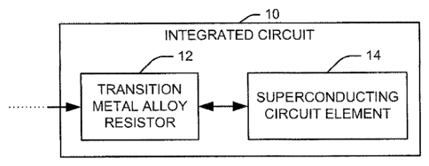
[0007] FIG. 1 illustrates a functional block diagram of an integrated
circuit in
accordance with an aspect of the present invention.
[0008] FIG. 2 illustrates an exemplary implementation of an integrated
circuit
assembly for use in milliKelvin temperature applications in accordance with an
aspect of the present invention.
[0009] FIG. 3 illustrates a circuit structure in its early stages of
fabrication.
[0010] FIG. 4 illustrates a schematic cross-sectional view of the
structure of
FIG. 3 after a photoresist material layer has been patterned in accordance
with an
aspect of the present invention.
[0011] FIG. 5 illustrates a schematic cross-sectional view of the
structure of
FIG. 4 after the etch step to extend openings in the superconductor material
layer in
accordance with an aspect of the present invention.
[0012] FIG. 6 illustrates a schematic cross-sectional view of the
structure of
FIG. 5 after undergoing a strip of the photoresist material layer in
accordance with an
aspect of the present invention.
[0013] FIG. 7 illustrates a schematic cross-sectional view of the
structure of
FIG. 6 after depositing a layer of resistive material.
2
CA 02858087 2014-06-03
WO 2013/137959 PCT/US2012/070066
[0014] FIG. 8 illustrates a schematic cross-sectional view of the
structure of
FIG. 7 after a second photoresist material layer is applied to cover the
structure and
patterned and developed to expose open regions.
[0015] FIG. 9 illustrates a schematic cross-sectional view of the
structure of
FIG. 8 after the exposed resistive material is etched away to expose the layer
of
superconducting material.
[0016] FIG. 10 illustrates a schematic cross-sectional view of the
structure of
FIG. 9 after the second photoresist material layer is stripped.
[0017] FIG. 11 illustrates a schematic cross-sectional view of the
structure of
FIG. 10 after an insulator layer has been deposited.
DETAILED DESCRIPTION
[0018] FIG. 1 illustrates a functional block diagram of an integrated
circuit 10
containing elements (e.g., 12) that are resistive in accordance with an aspect
of the
present invention. While it will be appreciated by one of skill in the art
that the
resistivity of materials will generally vary with the operating conditions,
particularly
temperature, materials having substantially no resistance in the operating
conditions
of a circuit are referred to herein as "superconducting materials."
Specifically, for the
purpose of this document, a superconducting material is a material having a
transition temperature (Tc) greater than an operating temperature of the
circuit. In
one implementation, the circuit can be used within an operating environment of
a
quantum circuit, such that the operating temperature is less than one hundred
milliKelvin.
[0019] The circuit 10 includes a resistor 12, formed from an alloy of
transition
metals that has significant resistance in an operating environment of the
circuit, and
at least one circuit element 14 formed from a superconducting material that is
superconducting in the operating environment. For example, the circuit element
14
can include any of a capacitor, a spiral inductor, a Josephson junction, or
any of a
number of other circuit elements commonly used in superconductor applications.
The superconducting material can include any metal, carbon allotrope, alloy,
ceramic, or other pure element known to exhibit superconductivity at low
3
CA 02858087 2014-06-03
WO 2013/137959 PCT/US2012/070066
temperatures. Since a number of materials possess this property at milliKelvin
temperatures, the superconducting material can be selected as a low cost
material
compatible with semiconductor processing techniques.
[0020] In accordance with an aspect of the present invention, the alloy
of
transition metals used to form the resistor 12 can be selected such that a
total ratio
of valance electrons to atoms within the alloyed material is within a
specified range.
Specifically, the alloy can exhibit normal conductivity when the ratio of
valance
electrons to atoms is greater than five and less than six. The term
"transition metal"
refers to any element found within the d-block of the periodic table,
specifically those
within Groups 3-11. By "valance electrons," it is meant the combined number of
electrons in the outermost s subshell and the outermost d subshell of a given
atom.
Accordingly, for the purpose of this application, the number of valance
electrons
associated with each atom is equal to four for the Group 4 transition metals,
five for
the Group 5 transition metals, and so on.
[0021] In one implementation, the metals forming the alloy can be
selected
from a group comprising titanium, vanadium, zirconium, niobium, molybdenum,
hafnium, tungsten, tantalum, and rhenium. The alloy can comprise two or more
than
two metals from that group, so long as the overall ratio of valance electrons
to atoms
falls between five and six. To ensure that the alloy has the desired
resistivity in the
milliKelvin range, an atomic ratio of the metals comprising the alloy can be
selected
to maintain a valance electrons to atoms ratio between about 5.35 to about
5.95. In
one implementation, the resistor 12 is designed to provide a sheet resistance
between one to ten ohms/square, and has a resistor-film thickness of twenty to
two
hundred nanometers. Accordingly, the film provides a resistivity of two to two
hundred micro-ohm-cm at the milliKelvin operating temperature. In one
implementation, the sheet resistance and thickness are selected to provide a
resistivity between ten and fifty micro-ohm-cm.
[0022] The use of the class of transition metal alloys described herein
allows
for a number of advantages. The described alloys have a sheet resistance
substantially independent of temperature in the 15 to 100 milliKelvin
operating
temperature range. They are non-magnetic and can be used in semiconductor
4
CA 02858087 2014-06-03
WO 2013/137959 PCT/US2012/070066
processing equipment without the risk of contaminating the semiconductor
equipment for other processes. As alloys, they are relatively insensitive to
minor
changes in impurities and defects, particularly when compared to pure
elements.
They are chemically stable at temperatures associated with semiconductor
processing, typically 130 to 300 C. This includes stability against chemical
reactions
as well as interdiffusion with neighboring film layers. This chemical
stability allows
for a low vapor pressure and resistance to corrosion. Many of these alloys can
be
applied with thin-film deposition processes that are consistent with other
portions of
the superconducting circuit fabrication process, and can be patterned via a
dry
etching process. Finally, the selected group of materials contains members
that are
relatively common and low cost.
[0023] FIG. 2 illustrates an exemplary implementation of an integrated
circuit
assembly 50 for use in milliKelvin temperature applications in accordance with
an
aspect of the present invention. The integrated circuit assembly 50 comprises
an
insulating substrate 52 that serves as a structural support for the assembly.
The
substrate 52 can be formed from any material having sufficient rigidity to
serve as a
substrate for a semiconductor circuit assembly that is an insulator at
milliKelvin
temperatures. In one implementation, the substrate 52 comprises a silicon
wafer.
[0024] A thin-film resistor 54 can be fabricated on the substrate. In
accordance with an aspect of the present invention, the resistor layer 54 can
be
formed from an alloy of transition metals having a specific ratio of valance
electrons
to atoms. In the illustrated implementation, the resistor 54 is fabricated
from an alloy
of titanium and tungsten, with an atomic ratio of tungsten to titanium of
approximately
five to one (i.e., approximately 17% of the atoms comprising the alloy are
tungsten
and approximately 83% are titanium). The selected alloy provides a sheet
resistance of 3.06 ohm/square, a thickness of 154 nm, and a resistivity of 47
micro-
ohm-cm. It will be appreciated, however, that these quantities can vary, for
example,
from a composition of 67% tungsten/33% titanium to a composition of 98%
tungsten/2% titanium. This corresponds to a range of compositions by weight
of 88.5% tungsten/11.5% titanium to 99.5% tungsten/0.5% titanium.
CA 02858087 2014-06-03
WO 2013/137959 PCT/US2012/070066
[0025] First and second superconducting traces 56 and 58 can be
fabricated
on the substrate 52 proximate to the thin film resistor 54. The
superconducting
traces 56 and 58 can be formed from aluminum, niobium, or some other
superconductor material. Each superconducting trace 56 and 58 is electrically
connected to the thin-film resistor 54 at respective terminals 62 and 64. The
entire
assembly can be covered by a second insulating layer 66. The use of the
titanium/tungsten alloy provides a number of advantages. The alloy exhibits a
negligible temperature dependance in its resistance at low temperatures. The
alloy
is not magnetic and does not contaminate the equipment for semiconductor
processing. Further, the deposition process can be performed at room
temperature
in argon gas, and a reactive ion etching process, using fluorine-based gases,
is well
established for the alloy.
[0026] Turning now to FIGS. 3-12, fabrication is discussed in connection
with
formation of a resistor for use in milliKelvin temperatures. It is to be
appreciated that
the present example is discussed with respect to a resistor, however, the
methodology can be employed for forming a variety of different devices for use
in a
low temperature environment. FIG. 3 illustrates a circuit structure 100 in its
early
stages of fabrication. FIG.3 represents the circuit structure after deposition
of a
superconducting material layer 102 on an insulating substrate 104. The
superconductor material layer 102 can be deposited via any appropriate
deposition
technique including Low Pressure Chemical Vapor Deposition (LPCVD), Plasma
Enhanced Chemical Vapor Deposition (PECVD), Atomic Layer Deposition (ALD),
sputtering or spin on techniques. In the illustrated implementation, the
superconducting material is deposited via sputtering. The material used to
fabricate
the superconductor material layer 102 can include, for example, aluminum,
niobium,
or some other superconductor material. The superconductor material layer 102
will
reside on another, insulator layer 104 that provides mechanical support for
the
superconductor material layer 102.
[0027] Next, as represented in FIG. 4, a photoresist material layer 108
is
applied to cover the structure and is then patterned and developed to expose
an
open region 110 in the photoresist material layer 108. The photoresist
material
6
CA 02858087 2014-06-03
WO 2013/137959 PCT/US2012/070066
layer 108 can have a thickness that varies in correspondence with the
wavelength of
radiation used to pattern the photoresist material layer 108. The photoresist
material
layer 108 may be formed over the superconductor material layer 102 via spin-
coating
or spin casting deposition techniques, selectively irradiated and developed to
form
the open region 110. The developer utilized in the developing of the
photoresist has
no effect on the protective barrier layer 106.
[0028] FIG. 5 illustrates the circuit structure 100 after performing an
etch step
on the superconductor material layer 102 to form an opening 114 in the
superconductor material layer 102. The etch can be, for example, a dry
chlorine
based plasma etch. For example, the superconductor material layer 102 can be
anisotropically etched with a plasma gas(es) containing chlorine ions, in a
commercially available etcher, such as a parallel plate Reactive Ion Etch
(RIE)
apparatus, Inductively Coupled Plasma (ICP) reactor or, alternatively, an
electron
cyclotron resonance (ECR) plasma reactor to replicate the mask pattern of the
patterned photoresist material layer 108 to thereby create the opening pattern
in the
superconductor material layer 102. Alternatively, the etch may be a wet etch.
Preferably, a selective etch technique is used to etch the superconductor
material
layer 102 at a relatively greater rate as compared to the patterned
photoresist
material layer and underlying layer (not shown).
[0029] The photoresist material layer 108 is then stripped (e.g., via
ashing in
an 02 plasma) so as to result in the structure shown in FIG. 6. FIG. 7
illustrates the
circuit structure 100 after depositing a layer of resistive material 122 over
the
structure of FIG. 6. In the illustrated implementation, the layer of resistive
material 122 is an alloy of titanium and tungsten having an atomic ratio of
approximately five to one, tungsten to titanium, and the layer is deposited
via
sputtering. Next, as represented in FIG. 8, a second photoresist material
layer 124
is applied to cover the structure and is then patterned and developed to
expose open
regions 126 in the second photoresist material layer 124.
[0030] In FIG. 9, the exposed resistive material 122 is etched away to
expose
the layer of superconducting material 102. The etch step can be a dry etch or
wet
etch that employs an etchant which selectively etches the protective barrier
layer 106
7
CA 02858087 2014-06-03
WO 2013/137959
PCT/US2012/070066
at a faster rate than the underlying superconducting material layer 102 and
the
overlying photoresist material layer 108. For example, resistive material 122
can be
anisotropically etched with a plasma gas(es), herein carbon tetrafloride (CF4)
containing fluorine ions, in a commercially available etcher, such as a
parallel plate
RI E apparatus or, alternatively, an electron cyclotron resonance (ECR) plasma
reactor to replicate the mask pattern of the patterned of the second
photoresist
material layer 124. In the illustrated implementation, the etching is
performed via
reactive ion etching with fluorine based gases. The second photoresist
material
layer 124 is then stripped to provide the structure shown in FIG. 10. In FIG.
11, the
circuit structure 100 is then covered with a second insulating layer 128, such
as
silicon or silicon oxide.
[0031] What
have been described above are examples of the invention. It is,
of course, not possible to describe every conceivable combination of
components or
methodologies for purposes of describing the invention, but one of ordinary
skill in
the art will recognize that many further combinations and permutations of the
invention are possible. For example, in the fabrication process illustrated in
FIGS. 3-12, the resistive layer can be deposited prior to the deposition of
the
superconducting layer, such that the resistive layer is directly between the
superconducting layer and the substrate at one or more locations. Accordingly,
the
invention is intended to embrace all such alterations, modifications, and
variations
that fall within the scope of this application, including the appended claims.
8