Note: Descriptions are shown in the official language in which they were submitted.
CA 02858153 2014-08-01
BI-LEVEL CURRENT CONFIGURABLE DRIVER
CROSS-REFERENCE TO RELATED APPLICATION
[0001] The present application claims priority of United States Provisional
Patent
Application No. 61/864,319, entitled "DRIVER FOR SOLID STATE LIGHT SOURCES",
filed on August 9, 2013, the entire contents of which are hereby incorporated
by
reference.
TECHNICAL FIELD
[0002] The present invention relates to lighting, and more specifically, to
drivers for
solid state light sources.
BACKGROUND
[0003] Solid state light sources, such as but not limited to light emitting
diodes (LEDs)
and other semiconductor-based light sources, require a constant direct current
(DC)
voltage or current to operate optimally. During operation, the light source
must be
protected from line-voltage fluctuations. Changes in voltage can produce a
disproportional change in current, which in turn can cause light output to
vary, as solid
state light source light output is proportional to current and is rated for a
current range.
If current exceeds the manufacturer recommendations, the output of the solid
state light
sources can become brighter, but that output can degrade at a faster rate due
to higher
temperatures within the device, which leads to a shorter useful life.
[0004] Solid state light sources, therefore, require a driver (also referred
to as a driver
circuit and/or a power supply) that converts incoming alternating current (AC)
power
to the proper DC voltage, and regulates the current flowing through the light
sources
during operation. The driver converts 120V (or other voltages) 60Hz AC power
to DC
1
CA 02858153 2014-08-01
power required by the light sources, and protects the light sources from line-
voltage
fluctuations.
[0005] Drivers can enable dimming of solid state light sources via, for
example, preset
commands, occupant presence, or other controls. Drivers with dimming
capability can
dim the light output over the full range from one hundred percent to zero
percent.
Dimming drivers can dim solid state light sources by, for example, reducing
the
forward current, pulse width modulation (PWM) via digital control, or more
sophisticated methods. Most dimming drivers operate using the PWM method. With
this method, the frequency could range from a hundred modulations per second
to as
high as hundreds of thousands of modulations per second, so that the solid
state light
source appears to a human eye to be continuously lighted without flicker. A
benefit of
the PWM method of dimming is that it enables dimming with minimal color shift
in the
light source output. Dimming does not result in a loss of efficiency. During
dimming,
the solid state light sources are still operated at the same voltage and
current as during
full light output. In addition, life of a lighting device including the solid
state light
sources is not affected by dimming, as is sometimes the case with frequently
dimmed
fluorescent lamps. Rather, dimming solid state light sources may lengthen
their useful
life, because dimming can reduce operating temperatures inside the light
source.
SUMMARY
[0006] Embodiments provide a bi-level current configurable driver for solid
state light
sources. The user has the option to set the output current via an isolated
external
resistor. The driver may be, and in some embodiments is, also used to dim the
solid
state light sources to less than the full load drive current when run in step-
dim mode
configuration, for example but not limited to 50% of its full load drive
current. This is
useful for providing flexibility in design and in the field where a single
hardware
version can be used for multiple configurations that require different
operating
currents.
2
CA 02858153 2014-08-01
[0007] In an embodiment, there is provided a hi-level current configurable
driver. The
hi-level current configurable driver includes: a driver circuit; a regulator
circuit; a
feedback circuit; a resistor divider comprising an upper resistor and a lower
resistor, the
resistor divider determining a reference current provided by the regulator
circuit,
wherein the upper resistor has a first lead connected to a voltage and a
second lead
connected to a first input of the regulator circuit, and wherein the lower
resistor has a
first lead connected to a ground and a second lead connected to the second
lead of the
upper resistor and a first input of the feedback circuit; and an external
resistor coupled
in parallel to the first input of the regulator circuit, wherein changing a
value of the
external resistor changes a value of the reference current.
[0008] In a related embodiment, the external resistor may be connected in
parallel with
the lower resistor. In another related embodiment, the external resistor may
be
connected in parallel with the upper resistor. In still another related
embodiment, the
driver circuit may include a constant current constant voltage (CCCV)
regulator. In a
further related embodiment, the bi-level current configurable driver may
further
include a step-dim circuit coupled between the regulator circuit and a load
including
one or more solid state light sources. In a further related embodiment, the
step-dim
circuit may include a first resistor connected in series between the load and
a second
input of the regulator circuit, a second resistor having a first end connected
to the
second input of the regulator circuit, a transistor having a source connected
to a second
end of the second resistor, a drain connected to the ground, and a gate
connected to an
output of a feedforward optocoupler, wherein when the transistor is off, the
second
input of the regulator circuit may see a full sense voltage and the driver
circuit may
provide full current at an output, and wherein when the transistor is on, the
second
input of the regulator circuit may see half of the sense voltage and may
provide a
reduced amount of current at an output. In another further related embodiment,
an
output of the regulator circuit may provide feedback to a primary side of the
driver
circuit.
3
CA 02858153 2014-08-01
,
[0009] In another embodiment, there is provided a step-dim circuit for a power
supply.
The step-dim circuit for a power supply includes: a feedback circuit coupled
to an
output of the power supply; a driver circuit receiving an output of the
feedback circuit,
the driver circuit providing a driver signal to a half bridge inverter of the
power supply;
a step-dim interface coupled to a first alternating current (AC) input line, a
second AC
input line, and a neutral line providing voltage to the power supply; and a
first
feedforward circuit coupled to the step-dim interface, wherein the first
feedforward
circuit receives a first signal from the step-dim interface based on the
states of the first
AC input line, the second AC input line, and the neutral line, and wherein the
first
feedforward circuit provides a second signal to the feedback circuit, the
feedback circuit
providing a feedback signal to the driver circuit, wherein when the feedback
signal is in
a first state, the power supply provides full current to a load, and when the
feedback
signal is in a second state, the power supply provides less than full current
to the load.
[00101 In a related embodiment, when the first AC input line, the second AC
input line,
and the neutral line are all on, the power supply may provide full current to
the load.
In another related embodiment, when the first AC input line is off, the second
AC input
line is on, and the neutral line is on, the power supply may provide a second
amount of
current to the load, the second amount of current less than the full amount of
current.
In still another related embodiment, when the first AC input line is on, the
second AC
input line is off, and the neutral line is on, the power supply may provide a
second
amount of current to the load, the second amount of current less than the full
amount of
current. In yet another related embodiment, when the first AC input line, the
second
AC input line, and the neutral line are all off, the power supply may provide
no current
to the load.
[0011] In still yet another related embodiment, the step-dim circuit for a
power supply
may further include a second feedforward circuit coupled to the step-dim
interface,
wherein the second feedforward circuit may receive a first signal from the
step-dim
interface based on the states of the first AC input line, the second AC input
line, and the
neutral line, and wherein the second feedforward circuit may provide a third
signal to
4
CA 02858153 2014-08-01
the feedback circuit. In a further related embodiment, when the first AC input
line, the
second AC input line, and the neutral are all on, the power supply may provide
full
current to the load. In another further related embodiment, when the first AC
input
line is off, the second AC input line is on, and the neutral line is on, the
power supply
may provide a second amount of current to the load, the second amount of
current less
than the full amount of current. In still another further related embodiment,
when the
first AC input line is on, the second AC input line is off, and the neutral
line is on, the
power supply may provide a third amount of current to the load, the third
amount of
current less than the second amount of current. In yet another further related
embodiment, when the first AC input line, the second AC input line, and the
neutral
line are all off, the power supply may provide no current to the load.
[00121 In another embodiment, there is provided a driver circuit. The driver
circuit
includes: an EMI front end coupled to a first alternating current (AC) line, a
second AC
line, and a neutral line, the EMI front end providing a rectified direct
current (DC)
voltage; a boost PFC circuit coupled to the EMI front end, the boost PFC
providing a
boosted voltage; an inverter coupled to the boost PFC circuit; an isolation
transformer
having a primary side coupled to the inverter; a rectifier coupled to a
secondary side of
the isolation transformer; an output filter coupled to the rectifier, an
output of the
rectifier capable of driving a load; a feedback circuit coupled to the load
and providing
an output of the driver circuit; a step-dim interface coupled to a first AC
line, a second
AC line, and a neutral line; and a first feedforward driver receiving an
output from the
step-dim interface and providing a signal to the feedback circuit.
[0013] In a related embodiment, when the first AC line, the second AC line,
and the
neutral line are all on, the driver circuit may provide full current to the
load, and
wherein when the first AC line is off, the second AC line is on, and the
neutral line is
on, the driver circuit may provide a second amount of current to the load, the
second
amount of current less than the full amount of current, and wherein when the
first AC
line is on, the second AC line is off, and the neutral line is on, the driver
circuit may
provide a second amount of current to the load, the second amount of current
less than
CA 02858153 2014-08-01
the full amount of current, and wherein when the first AC line, the second AC
line, and
the neutral line are all off, the driver circuit may provide no current to the
load. In
another related embodiment, the driver circuit may further include a second
feedforward circuit coupled to the step-dim interface, wherein the second
feedforward
circuit may receive a first signal from the step-dim interface based on the
states of the
first AC line, the second AC line, and the neutral line, wherein the second
feedforward
circuit may provide a third signal to the feedback circuit, and wherein when
the first
AC line, the second AC line, and the neutral line are all on, the driver
circuit may
provide full current to the load, wherein when the first AC line is off, the
second AC
line is on, and the neutral line is on, the driver circuit may provide a
second amount of
current to the load, the second amount of current less than the full amount of
current,
wherein when the first AC line is on, the second AC line is off, and the
neutral line is
on, the driver circuit may provide a third amount of current to the load, the
third
amount of current less than the second amount of current, and wherein when the
first
AC line, the second AC line, and the neutral line are all off, the driver
circuit may
provide no current to the load.
BRIEF DESCRIPTION OF THE DRAWINGS
[0014] The foregoing and other objects, features and advantages disclosed
herein will be
apparent from the following description of particular embodiments disclosed
herein, as
illustrated in the accompanying drawings in which like reference characters
refer to the
same parts throughout the different views. The drawings are not necessarily to
scale,
emphasis instead being placed upon illustrating the principles disclosed
herein.
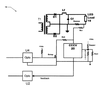
[0015] FIG. 1 depicts a schematic diagram of a first circuit used to set an
output current
of a power supply by way of an external resistor according to embodiments
disclosed
herein.
[0016] FIG. 2 depicts a schematic diagram of a first circuit used to provide a
step-dim
interface for a power supply according to embodiments disclosed herein.
6
CA 02858153 2014-08-01
[0017] FIG. 3 depicts a schematic diagram of a second circuit used to provide
a step-dim
interface for a power supply according to embodiments disclosed herein.
[0018] FIG. 4 depicts a graph of current versus resistance for a power supply
according
to embodiments disclosed herein.
DETAILED DESCRIPTION
[0019] Embodiments presented herein are based on an inductor capacitor
capacitor
(LCC) based resonant converter topology. The regulation of current is achieved
through frequency modulation of the LCC tank. Referring to FIG. 1, a portion
of a
driver 10 is shown. The output of an LCC tank (not shown) is provided to a
primary
side of an isolation transformer Ti. The isolation transformer T1 is used for
isolation,
and could provide a step up voltage, a step down voltage, or reflect the input
voltage at
the same level. The output of the isolation transformer Ti is followed by a
rectifier
comprising a diode D1 and a diode D2, which are followed by an LC filter
comprising an
inductor Lf and a capacitor Cf. The current from the LC filter is then
provided to an
LED load 18, which includes one or more solid state light sources (not
necessarily
limited to light emitting diodes).
[0020] An external resistor Rset is used to set the current of the driver 10
within a
specified current range. This is used to provide flexibility in design and in
the field
where a single hardware version can be used for multiple configurations that
require
different operating currents. A constant-voltage, constant-current (CCCV)
regulator 20
has an adjustable reference for a current loop. This fact is taken advantage
in using the
"Rset" interface. A resistive divider determines the reference for the
current. The
nominal value is determined by resistors Rupper and Rlower. The external
resistor Rset
is connected in parallel with the resistor Rlower (or alternately the resistor
Rupper),
thereby changing the value of the current reference. The value of the external
resistor
Rset thereby determines the constant current provided by the CCCV regulator
20.
Different values of the external resistor Rset result in different currents
provided to the
7
CA 02858153 2014-08-01
LED load 18, thereby permitting a single circuit design to provide a variety
of current
values for multiple different scenarios and/or loads.
[0021] The circuit of FIG. 1, in some embodiments, is further used for
providing a step-
dim function. To utilize the "on" signal for current reduction, a sense
network in the
current loop has been modified. Two equal value resistors (e.g., 25k ohms
each) RS1
and RS2 are connected in series across a low value sense resistor Rsense. The
common
point of the resistors RS1 and R52 is connected a feedback pin (CC-) of the
CCCV
regulator 20. The other end of the resistor RS1 is connected to the sense
resistor Rsense,
while the other end of the resistor RS2 is connected to a source of a
transistor Qstep. A
gate of the transistor Qstep is connected to ground, as is a drain of the
transistor Qstep.
When the transistor Qstep is off, the full sense voltage is seen by the CCCV
regulator 20.
When the transistor Qstep is on, a path through the transistor Qstep to ground
is
provided. When the transistor Qstep is on, the resistors RS1 and RS2 act as a
voltage
divider and only half of the sense voltage is seen by the CCCV regulator 20 as
feedback.
In other words, for the same current reference, the actual current is doubled
when the
transistor Qstep is on, than when it is off.
[0022] Referring now to FIG. 2, an embodiment of a step-dim driver 100 is
shown. The
essential function of a step-dim interface is to reduce output current by half
based on a
selective input configuration on the line, while transferring and utilizing
this
information on the secondary side where the actual current control loop
resides. A
step-dim interface on an input side works by detecting the differential signal
between
two hot lines. If only one of them is connected, the step-dim interface
produces a "high"
signal.
[0023] The step-dim driver 100 includes two alternating current (AC) input
lines Li and
L2, and a neutral line N. With both the AC input lines Li and L2 on, and with
the
neutral line N on, one hundred percent light output is provided to an LED load
118
(which, similar to the LED load 18 of FIG. 1, is not necessarily limited to
light emitting
diodes, but may and does in some embodiments include any type of solid state
light
source(s)). If the AC input line Li is off, and the AC input line L2 is on, a
reduced
8
CA 02858153 2014-08-01
amount (e.g., fifty percent) of light output is provided by the LED load 118.
If the AC
input line L2 is off, and the AC input line Li is on, a reduced amount of
light output is
provided by the LED load 118. With both the AC input lines Li and L2 off, and
with the
neutral line N also off, zero percent light output is provided by the LED load
118.
[0024] The AC voltage from the AC input lines Li and L2 along with the neutral
line N is
provided to an EMI filter and front end and rectifier 112, which provides a
rectified DC
voltage VREC. This rectified DC voltage VREC is provided to a boost PFC
circuit 114,
which outputs a boosted voltage (e.g., 450 volts DC). This boosted DC voltage
is fed
into an inverter 116, which includes a resonant network with an LCC tank
circuit. The
output of the inverter 116 is then provided to a primary side of an isolation
transformer
T1. The isolation transformer Ti is used for isolation, and could provide a
step up
voltage, a step down voltage, or reflect the input voltage at the same level.
[0025] The output of the isolation transformer Ti is followed by a rectifier
comprising
diodes Di and D2, which is followed by an output filter 119. The current from
the
output filter 119 is then provided to the LED load 118. All of the above
described
circuitry is driven by an application specific integrated circuit (ASIC) 122,
also referred
to herein as a driver circuit 122. The driver circuit 122 comprises a constant
current
constant coltage (CCCV) regulator and is used to set the current to a certain
value and
sets the output voltage to a certain value. The driver circuit 122 provides
the gate drive
for the boost PFC circuit 114 and the gate drive for the inverter 116. The
driver circuit
122 also provides additional functionality, such as but not limited to
protection.
[0026] Feedback from an optocoupler 120 on the secondary side of the
transformer Ti is
used. The optocoupler 120 provides isolation and is less expensive than an
additional
transformer. The constant current-constant voltage regulator of the driver
circuit 122 is
used for modulation and providing feedback through the optocoupler 120. The
driver
circuit 122 normally operates in constant current mode and a voltage loop is
present to
limit the output voltage in abnormal/fault conditions. For step-dimming
functions, in
some embodiments, the circuit 100 is initially running at one hundred percent.
A step-
dim interface 126 is connected to the AC input lines Li and L2 and the neutral
line N on
9
CA 02858153 2014-08-01
its input. The step-dim interface 126 provides an output to a feedforward
optocoupler
124. The feedforward optocoupler 124 has an output connected to the feedback
optocoupler 120. When the step-dim interface 126 determines there is a need to
provide
a dimming function, the feedforward optocoupler 124 provides a signal to the
feedback
optocoupler 120 to reduce the current by a certain amount (e.g., one half).
The feedback
optocoupler 120 will add another resistor (not shown) in parallel to a set
resistor Rset,
which will configure the current to fifty percent of its original value. The
frequency
provided by the driver circuit 122 to the half bridge inverter 116 will thus
be bumped
up. The higher the frequency to the half bridge inverter 116, the lower the
current to the
LED load 118. Accordingly, when the AC input lines Li and L2 are both on, the
step-
dim driver 100 operates at maximum current. When either one (but not both) of
the AC
input lines Li or L2 are on, the step-dim driver 100 operates at a reduced
current (e.g.,
fifty percent). When both of the AC input lines Li and L2 are off, the step-
dim driver
100 produces zero current.
[0027] Referring now to FIG. 3, a further embodiment of a step-dim circuit 200
is shown.
In this embodiment, two feedforward circuits 224 and 228 are used instead of
one
(shown in FIG. 2). A step-dim interface 226 on the input side works by
detecting the
differential signal between the two AC input lines Li and L2 and, dependent on
which
ones are on, provides a signal to feedforward circuits 224 and 228.
[0028] For step-dimming functions, assume the step-dim circuit 200 is
initially running
at 100%. The step-dim interface 226 is connected between the AC input lines L1
and L2
and a neutral line N, and a first feedforward optocoupler 224 and a second
feedforward
optocoupler 228. Both feedforward optocouplers 224 and 228 have an output
connected
to a feedback circuit 220. When the step-dim interface 226 determines there is
a need to
provide a dimming function, the feedforward optocouplers 224 and/or 226
provides a
signal to the feedback circuit 220 to reduce the current by a certain amount.
The
feedback circuit 220 will add in a resistance in parallel to a set resistor
Rset, which will
configure the current to a certain percentage of its original value. The
frequency
provided by a driver circuit 222 to the half bridge inverter 216 will be
bumped up. The
CA 02858153 2014-08-01
higher the frequency to the half bridge inverter 216, the lower the current to
an LED
load 218 (which, like the LED load 118 of FIG. 2, is not necessarily limited
to light
emitting diodes). Accordingly, when the AC input lines L1 and L2 are both on,
the step-
dim circuit 200 operates at maximum current. When the AC input line L1 is on
and the
AC input line L2 is off, the step-dim circuit 200 operates at a reduced
current (e.g., sixty
percent). When the AC input line L1 is off and the AC input line L2 is on, the
step-dim
circuit 200 operates at a further reduced current (e.g., thirty percent). When
both the
AC input lines Li and L2 are off, the step-dim circuit 200 produces zero
current.
[0029] FIG. 4 shows a graph 300 with a horizontal axis showing resistance in
kiloohms
for values of the set resistor Rset of FIGs. 2 and 3, and a vertical axis
showing current in
amps for the output of a driver circuit. A first line 302 shows the
relationship of the
nominal current (full value) dependent upon the Rset resistance. Also shown is
the
relationship of the step-dim current dependent upon the Rset resistance. The
step-dim
current is generally half the value of the nominal current for the various
resistances of
Rset.
[0030] The methods and systems described herein are not limited to a
particular
hardware or software configuration, and may find applicability in many
computing or
processing environments. The methods and systems may be implemented in
hardware
or software, or a combination of hardware and software. The methods and
systems
may be implemented in one or more computer programs, where a computer program
may be understood to include one or more processor executable instructions.
The
computer program(s) may execute on one or more programmable processors, and
may
be stored on one or more storage medium readable by the processor (including
volatile
and non-volatile memory and/or storage elements), one or more input devices,
and/or
one or more output devices. The processor thus may access one or more input
devices
to obtain input data, and may access one or more output devices to communicate
output data. The input and/or output devices may include one or more of the
following: Random Access Memory (RAM), Redundant Array of Independent Disks
(RAID), floppy drive, CD, DVD, magnetic disk, internal hard drive, external
hard drive,
11
CA 02858153 2014-08-01
,
memory stick, or other storage device capable of being accessed by a processor
as
provided herein, where such aforementioned examples are not exhaustive, and
are for
illustration and not limitation.
[0031] The computer program(s) may be implemented using one or more high level
procedural or object-oriented programming languages to communicate with a
computer system; however, the program(s) may be implemented in assembly or
machine language, if desired. The language may be compiled or interpreted.
[0032] As provided herein, the processor(s) may thus be embedded in one or
more
devices that may be operated independently or together in a networked
environment,
where the network may include, for example, a Local Area Network (LAN), wide
area
network (WAN), and/or may include an intranet and/or the internet and/or
another
network. The network(s) may be wired or wireless or a combination thereof and
may
use one or more communications protocols to facilitate communications between
the
different processors. The processors may be configured for distributed
processing and
may utilize, in some embodiments, a client-server model as needed.
Accordingly, the
methods and systems may utilize multiple processors and/or processor devices,
and
the processor instructions may be divided amongst such single- or multiple-
processor/ devices.
[0033] The device(s) or computer systems that integrate with the processor(s)
may
include, for example, a personal computer(s), workstation(s) (e.g., Sun, HP),
personal
digital assistant(s) (PDA(s)), handheld device(s) such as cellular
telephone(s) or smart
cellphone(s), laptop(s), handheld computer(s), or another device(s) capable of
being
integrated with a processor(s) that may operate as provided herein.
Accordingly, the
devices provided herein are not exhaustive and are provided for illustration
and not
limitation.
[0034] References to "a microprocessor" and "a processor", or "the
microprocessor" and
"the processor," may be understood to include one or more microprocessors that
may
communicate in a stand-alone and/or a distributed environment(s), and may thus
be
configured to communicate via wired or wireless communications with other
12
CA 02858153 2014-08-01
processors, where such one or more processor may be configured to operate on
one or
more processor-controlled devices that may be similar or different devices.
Use of such
"microprocessor" or "processor" terminology may thus also be understood to
include a
central processing unit, an arithmetic logic unit, an application-specific
integrated
circuit (IC), and/or a task engine, with such examples provided for
illustration and not
limitation.
[0035] Furthermore, references to memory, unless otherwise specified, may
include one
or more processor-readable and accessible memory elements and/or components
that
may be internal to the processor-controlled device, external to the processor-
controlled
device, and/or may be accessed via a wired or wireless network using a variety
of
communications protocols, and unless otherwise specified, may be arranged to
include
a combination of external and internal memory devices, where such memory may
be
contiguous and/or partitioned based on the application. Accordingly,
references to a
database may be understood to include one or more memory associations, where
such
references may include commercially available database products (e.g., SQL,
Informix,
Oracle) and also proprietary databases, and may also include other structures
for
associating memory such as links, queues, graphs, trees, with such structures
provided
for illustration and not limitation.
[0036] References to a network, unless provided otherwise, may include one or
more
intranets and/or the internet. References herein to microprocessor
instructions or
microprocessor-executable instructions, in accordance with the above, may be
understood to include programmable hardware.
[0037] Unless otherwise stated, use of the word "substantially" may be
construed to
include a precise relationship, condition, arrangement, orientation, and/or
other
characteristic, and deviations thereof as understood by one of ordinary skill
in the art,
to the extent that such deviations do not materially affect the disclosed
methods and
systems.
[0038] Throughout the entirety of the present disclosure, use of the articles
"a" and/or
"an" and/or "the" to modify a noun may be understood to be used for
convenience and
13
CA 02858153 2014-08-01
to include one, or more than one, of the modified noun, unless otherwise
specifically
stated. The terms "comprising", "including" and "having" are intended to be
inclusive
and mean that there may be additional elements other than the listed elements.
[0039] Elements, components, modules, and/or parts thereof that are described
and/or
otherwise portrayed through the figures to communicate with, be associated
with,
and/or be based on, something else, may be understood to so communicate, be
associated with, and or be based on in a direct and/or indirect manner, unless
otherwise stipulated herein.
[0040] Although the methods and systems have been described relative to a
specific
embodiment thereof, they are not so limited. Obviously many modifications and
variations may become apparent in light of the above teachings. Many
additional
changes in the details, materials, and arrangement of parts, herein described
and
illustrated, may be made by those skilled in the art.
14