Note: Descriptions are shown in the official language in which they were submitted.
1
SYSTEM, CONTROLLER, AND METHOD FOR DETERMINING
CONDUCTANCE OF AN OBJECT
[0001] This paragraph removed intentionally
FIELD
[0002] The field of the invention relates generally to
monitoring systems and more specifically to system, controller, and
method for determining conductance of an object or material.
BACKGROUND
[0003] Some known measurement systems measure a
conductivity of a specimen of interest by placing electrodes into
contact with the specimen. A voltage is applied to the electrodes
and a resulting current is measured. The conductivity is then
computed from the measured current. In some cases, many electrodes
are attached to the specimen so that a type of imaging is made
possible, provided that conductivity varies spatially through the
specimen. This latter condition is true for geological specimens
and human tissue specimens.
[0004] An alternative is to generate eddy currents
within the specimen through inductive coupling to an external coil.
The eddy currents exist in proportion to the local conductivity of
the material and can be detected in a number of ways. For example,
an amount of electrical energy
CA 2858527 2018-12-07
CA 02858527 2014-06-06
WO 2013/084091
PCT/IB2012/056128
2
dissipated in the coil may be measured when the coil is
placed near a specimen.
[0005] The eddy currents are typically generated
using a probe or a sensor that oscillates in a resonance
state. A phase-locked-loop (PLL) circuit may be included in
the probe to automatically tune the probe such that the probe
is maintained in the resonant state. In addition, such
probes may require additional components to maintain the
resonant state or to detect the energy dissipated, such as a
peak detector and/or a variable resistor. The PLL circuitry
and the additional components may undesirably increase a size
and a cost of the probe.
[0006] Thus, there remains a need for systems
and methods that non-invasively determine the conductance of
an object in a cost-effective, accurate, and efficient
manner.
SUMMARY
[0007] In one aspect, a system for determining a
conductance of an object generally comprises a sensor
configured to emit an electromagnetic field when an
excitation signal is received, wherein the electromagnetic
field interacts with the object when the object is positioned
within the electromagnetic field. A signal processing
circuit is coupled to the sensor and configured to provide an
adjustable capacitance to the sensor to adjust a phase angle
of a current flowing through the sensor, to generate a
voltage measurement representative of a voltage across the
sensor, and to generate a current measurement representative
of the current flowing through the sensor. A controller is
coupled to the signal processing circuit and configured to
CA 02858527 2014-06-06
WO 2013/084091
PCT/IB2012/056128
3
calculate an admittance of the sensor based on the voltage
measurement and the current measurement, and to determine a
conductance of the object based on the calculated admittance
of the sensor.
[0008] In another aspect, a method of
determining a conductance of an object generally comprises
emitting an electromagnetic field towards an object such that
the electromagnetic field interacts with the object. A phase
angle of a current flowing through the sensor is adjusted
using an adjustable capacitive element coupled to the sensor.
A voltage measurement representative of a voltage across the
sensor and a current measurement representative of the
current flowing through the sensor are generated. An
admittance of the sensor is calculated based on the voltage
measurement and the current measurement, and a conductance of
the object is determined based on the calculated admittance
of the sensor.
[0009] In still another aspect, a controller for
determining a conductance of an object generally comprises a
processor and a memory device coupled to the processor. The
memory device is configured to store a plurality of program
modules including a phase angle calculator module executable
by the processor to receive a current measurement
representative of a current flowing through a sensor, and
calculate a phase angle of the current flowing through the
sensor. The program modules also include an impedance
calculator module executable by the processor to receive the
current measurement, receive a voltage measurement
representative of a voltage across the sensor, and calculate
an impedance of the sensor based on the current measurement
and the voltage measurement. The program modules further
include an admittance calculator module executable by the
CA 02858527 2014-06-06
WO 2013/084091
PCT/IB2012/056128
4
processor to calculate an admittance of the sensor based on
the calculated phase angle and the calculated impedance, and
a conductance calculator module executable by the processor
to determine a conductance of the object based on the
calculated admittance of the sensor.
BRIEF DESCRIPTION OF THE DRAWINGS
[0010] Figure 1 is a block diagram of one
embodiment of a monitoring system that can be used to
determine a conductance of an object.
[0011] Figure 2A is a top view of a sensor
suitable for use with the monitoring system of Figure 1.
[0012] Figure 2B is a schematic view of a
circuit representing electrical characteristics of the sensor
of Figure 2A.
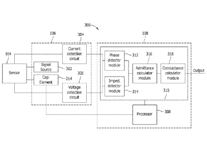
[0013] Figure 3 is a block diagram of the
monitoring system illustrated in Figure 1.
[0014] Figure 4 is a schematic diagram of an
analog portion of a signal processing circuit suitable for
use with the monitoring system illustrated in Figure 3.
[0015] Figure 5 is a graph of a calibration plot
that can be generated and used by the monitoring system.
[0016] Figure 6 is a flowchart illustrating a
method of determining a conductance of an object using the
monitoring system.
[0017] Figure 7 is a graph of an admittance of
the object measured by the monitoring system.
CA 02858527 2014-06-06
WO 2013/084091
PCT/IB2012/056128
[0018] Corresponding reference characters
indicate corresponding parts throughout the drawings.
DETAILED DESCRIPTION OF THE DRAWINGS
[0019] Figure 1 is a block diagram of one
suitable embodiment of a monitoring system, indicated
generally at 100, that can be used to determine or monitor a
conductance of an object 102. In one suitable embodiment,
the monitoring system 100 is used to non-invasively determine
and/or monitor a conductance (or conductivity) at one or more
locations on a person's body for use in determining a
condition or diagnosing a disease of the person, e.g.,
vascular disease.
[0020] The monitoring system 100 includes a
sensor 104 coupled to a signal processing circuit 106, and a
controller 108 coupled to the signal processing circuit. In
one suitable embodiment, the monitoring system 100 may be
enclosed within a housing 110 to protect the components of
the system. The housing 110 may be positioned in close
proximity to the object 102 such that a gap 112 is defined
between the sensor 104 and the object 102.
[0021] During operation, the signal processing
circuit 106 generates a fixed frequency excitation signal and
transmits the excitation signal to the sensor 104. The
excitation signal causes the sensor 104 to emit an
electromagnetic field, indicated generally at 114. When the
sensor 104 is placed in close proximity to the object 102,
the field 114 traverses the gap 112 and interacts with the
object, causing eddy currents to be formed within the object.
The interaction of the field 114 and the object 102 usually
causes a shift in the phase angle of a signal received from
CA 02858527 2014-06-06
WO 2013/084091
PCT/IB2012/056128
6
the sensor 104 (e.g., a current flowing through the sensor)
due to stray capacitance developing across the sensor while
the sensor is in proximity to the object being tested or
monitored. Specifically, the current through the sensor 104
and the voltage across the sensor may not reach their
respective maximum values at the same time. Accordingly, the
phase angle refers to the difference between the time that
the current flowing through the sensor 104 reaches the
maximum value and the time that the voltage across the sensor
reaches the maximum value. A zero phase angle indicates a
resonant condition of the sensor 104.
[0022] In addition, the signal received from the
sensor 104 may be attenuated, causing an amplitude of the
signal to be reduced as compared to an amplitude of the
excitation signal. The attenuation of the signal causes an
effective impedance to be induced to the sensor 104. As
described more fully herein, the signal processing circuit
106 measures the current and the voltage of the signal
received from the sensor 104 and transmits the measured
current and voltage to the controller 108.
[0023] The controller 108 detects the phase
angle of the signal received from the sensor 104 and detects
an impedance of the sensor based on the voltage and the
current measurements received from the signal processing
circuit 106. In addition, the controller 108 calculates an
admittance of the sensor 104 and uses the calculated
admittance to determine the conductance of the object 102.
The conductance of the object 102 can be used to determine
one or more characteristics or conditions of the object.
CA 02858527 2014-06-06
WO 2013/084091
PCT/IB2012/056128
7
[0024] Figures 2A and 23 illustrate a sensor 104
suitable for use with the monitoring system 100 shown in
Figure 1. More specifically, Figure 2A is a top view of the
sensor 104, and Figure 23 is a schematic view of a circuit
200 representative of the electrical characteristics of the
sensor.
[0025] As seen in Figure 2A, the sensor 104
includes a sensor body 206 having a substantially planar
surface 204. A substantially spiral-shaped conductor 202 (or
"coil") is coupled to the substantially planar surface 204 of
the sensor body 206. In one suitable embodiment, the sensor
body 206 is a printed circuit board (PCB). For example, the
sensor body 206 may be a dual-layer PCB that includes the
conductor 202 positioned within a first layer and an
additional conductor (not shown) arranged in a spiral shape,
staggered or interleaved with respect to the conductor 202,
and positioned within the second layer. In other
embodiments, the sensor body 206 can be other substrates that
enable the conductor 202 to be coupled thereto.
[0026] As seen in Figure 2B, the conductor 202
is represented as an inductor 208 (L) coupled in series with
a first resistive element 210 (R.). The conductor 202 and
the first resistive element 210 are coupled in parallel with
a second resistive element 212 (Rp) and a capacitive element
214.
[0027] In one suitable embodiment, the first
resistive element 210 represents an effective resistance
added or induced into the sensor 104 as a result of the eddy
currents interacting with the object 102. The second
resistive element 212 is a resistor coupled to the sensor 104
to reduce a "Q" factor of the sensor 104 as desired. It
CA 02858527 2014-06-06
WO 2013/084091
PCT/IB2012/056128
8
should be recognized that, while the second resistive element
212 may be selected to have any suitable resistance, the
second resistive element has a much higher resistance than
the resistance of the first resistive element 210. For
example, the second resistive element 212 may have a
resistance that is about 1,000 times higher, 10,000 times
higher, or even higher, than the resistance of the first
resistive element 210.
[0028] The capacitive element 214 is coupled to
the sensor 104 to adjust a phase angle of the signal received
from the sensor and/or the current flowing through the
sensor. In one suitable embodiment, the capacitive element
214 is an adjustable capacitor (also known as a "trimmer")
that enables a user or a device such as the controller 108 to
adjust the capacitance of the capacitive element 214. It
should be recognized that the capacitive element 214 may be
represented as a plurality of capacitive components coupled
together in parallel. For example, a first capacitive
component 216 represents an amount of capacitance attributed
to the conductor 202, a second capacitive component 218
represents a capacitance shunted across the conductor 202 as
a result of an interaction with the conductor 202 and an
object 102 positioned proximate to the conductor 202, and a
third capacitive component 220 represents the adjustable
capacitance described above that enables the user or the
controller 108 to adjust the capacitance of the capacitive
element 214.
[0029] In one suitable embodiment, the
monitoring system 100 measures the shunted capacitance across
the conductor 202 (i.e., the capacitance represented by the
second capacitive component 218). The user or controller 108
adjusts or "sweeps" the value of the capacitive element 214
CA 02858527 2014-06-06
WO 2013/084091
PCT/IB2012/056128
9
(i.e., third capacitive component 220) throughout a
capacitance range of the capacitive element 214 while
measuring a phase angle (or a corrected phase angle as
described below) of the signal received from the sensor 104
at each capacitance value. The adjustment of the capacitive
element 214 (also referred to as a "capacitive sweep") is
performed a first time with the object near the conductor 202
(i.e., within the electromagnetic field 114 generated by the
conductor) and a second time without the object near the
conductor (i.e., not within the electromagnetic field
generated by the conductor). The controller 108 compares the
capacitance values required to produce resonance (e.g., a
phase angle of substantially zero) during the two capacitive
sweeps to determine a difference between the capacitances.
An amount of capacitance required to produce resonance when
no object is near the conductor 202 is more than the amount
of capacitance required when the object is near the
conductor. The difference in capacitance values is the
amount of capacitance arising from the interaction between
the conductor 202 and the object 102, and is further related
to the physical condition or state of the object.
[0030] Figure 3 is a simplified block diagram,
indicated generally at 300, of the monitoring system 100
shown in Figure 1. Figure 4 schematically illustrates an
analog portion of one exemplary signal processing circuit 400
of the monitoring system 100.
[0031] As seen in Figure 3, the sensor 104 is
coupled to the capacitive element 214 and to a signal source
302. In one suitable embodiment, the capacitive element 214
and the signal source 302 are positioned within the signal
processing circuit 106. Alternatively, the capacitive
element 214 and/or the signal source 302 may be positioned
CA 02858527 2014-06-06
WO 2013/084091
PCT/IB2012/056128
within the sensor 104 or external to both the sensor and the
signal processing circuit 106.
[0032] The signal processing circuit 106
includes a current detection circuit 304 and a voltage
detection circuit 306. The current detection circuit 304
detects or measures a current flowing through, or output
from, the sensor 104. In one suitable embodiment, the
current detection circuit 304 generates an output signal
(hereinafter referred to as a "current measurement signal")
having a voltage that is proportional to the measured current
flowing through the sensor 104. The voltage detection
circuit 306 detects or measures a voltage across the sensor
104, or a voltage output from the sensor. In a suitable
embodiment, the voltage detection circuit 306 generates an
output signal (hereinafter referred to as a "voltage
measurement signal") having a voltage that is proportional to
the measured voltage across the sensor 104. The current
measurement signal and the voltage measurement signal are
transmitted to the controller 108.
[0033] The controller 108 includes a processor
308 and a memory device 310 operatively connected to the
processor. The processor 308 includes any suitable
programmable circuit including one or more systems and
microcontrollers, microprocessors, reduced instruction set
circuits (RISC), application specific integrated circuits
(ASIC), programmable logic circuits (PLC), field programmable
gate arrays (FPGA), and any other circuit capable of
executing the functions described herein. The above examples
are exemplary only, and thus are not intended to limit in any
way the meaning of the term "processor". In a suitable
embodiment, the processor 308 is operatively coupled to the
CA 02858527 2014-06-06
WO 2013/084091
PCT/IB2012/056128
11
capacitive element 214 to control or adjust the capacitance
of the capacitive element.
[0034] The memory device 310 includes a computer
readable storage medium, such as, without limitation, random
access memory (RAM), flash memory, a hard disk drive, a solid
state drive, a diskette, a flash drive, a compact disc, a
digital video disc, and/or any suitable memory. In a
suitable embodiment, the memory device 310 includes data
and/or instructions that are executable by the processor 308
such that the processor 308 is programmed by the instructions
to enable the processor 308 to perform the functions
described herein.
[0035] In addition, the memory device 310
includes a plurality of computer-executable program modules
that are executed by the processor 308. The program modules
include a phase detector module 312, an impedance detector
module 314, an admittance calculator module 316, and a
conductance calculator module 318. Alternatively, one or
more of the program modules, such as the phase detector
module 312, may be implemented by a circuit or a device
separate from the processor 308.
[0036] In a suitable embodiment, the phase
detector module 312 detects a phase angle of the sensor 104
(e.g., of the current flowing through the sensor) based on
the current measurement signal and the voltage measurement
signal received from the signal processing circuit 106.
Specifically, the phase detector module 312 detects a phase
shift or phase angle between the current measurement signal
and the voltage measurement signal, and generates a signal or
value (hereinafter referred to as a "sensor phase angle")
representative of the detected phase shift or phase angle
CA 02858527 2014-06-06
WO 2013/084091
PCT/IB2012/056128
12
between the voltage measurement signal and the current
measurement signal. In one suitable embodiment, as described
more fully herein, the processor 308 calculates a phase angle
correction value for adjusting the sensor phase angle.
[0037] The impedance detector module 314 detects
an effective impedance of the sensor 104 (e.g., an impedance
of the effective sensor circuit 200 shown in Figure 23).
Specifically, the impedance detector module 314 divides the
root mean square (RMS) voltage measured across the sensor 104
(hereinafter referred to as the "sensor voltage"), as
represented by the voltage measurement signal, by the RMS
current flowing through the sensor (hereinafter referred to
as the "sensor current"), as represented by the current
measurement signal, to obtain the effective impedance of the
sensor (hereinafter referred to as the "sensor impedance").
In some embodiments, the sensor voltage and the sensor
current can be based on instantaneous voltage and current
values obtained from a waveform of the voltage across the
sensor 104 and the current flowing through the sensor.
[0038] The admittance calculator module 316
calculates the admittance of the sensor 104 based on the
sensor phase angle (as adjusted by the phase angle correction
value) and the sensor impedance. For example, as described
more fully herein, the admittance calculator module 316
calculates the admittance of the sensor by dividing the
cosine of the sensor phase angle (as adjusted by the phase
angle correction value) by the sensor impedance.
[0039] The conductance calculator module 318
determines or calculates a conductance of the object 102
based on the calculated admittance of the sensor 104. For
example, in a suitable embodiment, the conductance calculator
CA 02858527 2014-06-06
WO 2013/084091
PCT/IB2012/056128
13
module 318 determines the conductance of the object 102 by
referencing a calibration plot, described more fully herein,
to determine the conductance value corresponding to the
calculated admittance value of the sensor 104. The
conductance of the object 102, the admittance of the sensor
104, and/or any other values determined or calculated by the
controller 108 may be output, for example, to a display or to
a storage device.
[0040] As illustrated in Figure 4, the signal
source 302 is coupled in parallel with the second resistive
element 212, the capacitive element 214, and the sensor
circuit 200 (including inductor 208 and first resistive
element 210) that are described above with reference to
Figure 23. The signal source 302 is also coupled in series
with a current sense resistor 402 for use in detecting the
current flowing through sensor 104 (i.e., the sensor current
described above). The signal source 302 is an alternating
current (AC) source that provides an AC excitation signal to
sensor 104. In one suitable embodiment, the signal source
302 is, or includes, a Colpitts crystal oscillator that
oscillates at a predetermined frequency, such as at about 12
megahertz (MHz) or at any other suitable frequency.
[0041] In a suitable embodiment, the current
detection circuit 304 is coupled across the current sense
resistor 402 to measure the voltage drop across the current
sense resistor. In one suitable embodiment, the current
detection circuit 304 includes a pair of amplifiers, such as
a pair of operational amplifiers (op-amps). The current
detection circuit 304 generates a first output 404 of the
signal processing circuit 400 (i.e., the current measurement
signal) that has a voltage proportional to the current
flowing through sensor 104.
CA 02858527 2014-06-06
WO 2013/084091 PCT/IB2012/056128
14
[0042] In a suitable embodiment, the voltage
detection circuit 306 is coupled across the second resistive
element 212 to measure the voltage drop across the second
resistive element 212, and therefore, the voltage drop across
the sensor 104. In one suitable embodiment, the voltage
detection circuit 306 includes a pair of amplifiers, such as
a pair of op-amps. The voltage detection circuit 306
generates a second output 406 of the signal processing
circuit 400 (i.e., the current measurement signal) that has a
voltage proportional to the voltage across sensor 104.
[0043] During operation, signal processing
circuit 400 is used to facilitate determining the conductance
of the object 102 by calculating the admittance of the sensor
104. Specifically, the admittance (Y) of the sensor 104 is:
Y=G+jB Equation 1
where G is the real part of the admittance Y, and B is the
imaginary part (susceptance) of the admittance Y. In a
suitable embodiment, only the real part G of the admittance
is used herein, and the imaginary part B of the admittance is
disregarded. Accordingly, as used herein, the term
-admittance- refers to the real part G of the admittance Y,
unless otherwise specified.
[0044] The admittance G of the sensor 104 is
obtained by computing G from the equation:
cose 1
G=
= Equation 2
D D2 __ co2L2
s
where 6 is the phase angle of the sensor (i.e., the phase
angle of the signal output from the sensor), Z is the
impedance of the sensor, Rs is the resistance of the second
resistive element 212, Rs is the effective resistance of the
CA 02858527 2014-06-06
WO 2013/084091
PCT/IB2012/056128
first resistive element 210, co is the frequency of the sensor
(i.e., the frequency of the signal output from the sensor),
and L is the inductance of sensor (i.e., of inductor 208).
[0045] Referring to Equation 2, Rs is typically
small in comparison to the term w2L2 and, in some
embodiments, may be disregarded, or approximated to be zero
next to the term co2L2. Accordingly, as the inductance L is
constant, the admittance is modeled to be substantially
linear with respect to 1/02. In other words, the admittance
of the sensor 104 can be calculated at many suitable
frequencies, and, in contrast to prior art systems, is not
limited to only being calculated at or near a resonance
frequency, or in a resonant state, of the sensor 104.
[0046] Accordingly, to calculate the admittance
of the sensor 104, the sensor phase angle and the sensor
impedance are calculated as described above. The processor
308 calculates the cosine of the sensor phase angle and
divides the result by the sensor impedance to calculate the
admittance of the sensor.
[0047] However, the measurement of the phase
angle may need to be adjusted or calibrated due to additional
phase shifting resulting from other circuit components.
Accordingly, in a suitable embodiment, a phase angle
correction value is determined before calculating the
admittance of the sensor 104. First, the capacitive element
214 is adjusted to a high capacitive value, such as a highest
capacitive value that the capacitive element is able to
provide. The phase angle (hereinafter referred to as the
-high capacitance phase angle") of the sensor 104 is measured
as described above, and the phase angle correction value is
set to about 90 degrees plus the high capacitance phase
CA 02858527 2014-06-06
WO 2013/084091
PCT/IB2012/056128
16
angle. In an ideal situation with ideal components, the
phase angle correction value would be zero.
[0048] The capacitive element 214 is then
adjusted (i.e., the capacitance coupled across the sensor 104
is adjusted) until the phase angle of the sensor minus the
phase angle correction value is within a predefined phase
angle window. In one suitable embodiment, the phase angle
window is between about -70 degrees and about +70 degrees.
In a further embodiment, the phase angle window excludes a
predefined resonance phase angle window that is between about
-3 degrees and about +3 degrees. Accordingly, in such an
embodiment, the phase angle window may include phase angles
between about -70 degrees and about -3 degrees, and between
about +3 degrees and about +70 degrees. Alternatively, the
phase angle window and/or the resonance phase angle window
may include any other upper or lower boundaries to enable the
monitoring system 100 to function as described herein.
[0049] When the phase angle, as adjusted by the
phase angle correction value (i.e., the phase angle minus the
phase angle correction value) is within the predefined phase
angle window, the processor 308 calculates the admittance of
the sensor 104 as described above, e.g., by dividing the
cosine of the adjusted sensor phase angle by the sensor
impedance. The processor 308 determines the conductance of
the object 102 by referencing a calibration plot of the
sensor 104. Accordingly, as described herein, the monitoring
system 100 (e.g., the processor 108) may calculate the
admittance of the sensor 104 and may determine the
conductance of the object 102 while the sensor is not in a
resonant state.
CA 02858527 2014-06-06
WO 2013/084091
PCT/IB2012/056128
17
[0050] Figure 5 graphically illustrates an
exemplary calibration plot, indicated generally at 500, that
may be generated and/or used by the monitoring system 100.
The abscissa axis of calibration plot 500 represents a
conductance (or conductivity) 502 of one or more objects, and
the ordinate axis represents an admittance 504 of the sensor
104 as determined by the monitoring system 100. In a
suitable embodiment, all measurements represented within the
calibration plot 500 are obtained using a single fixed
frequency for the sensor excitation signal.
[0051] In a suitable embodiment, the calibration
plot 500 is generated to calibrate the monitoring system 100.
For example, the calibration plot 500 is generated to
identify the correlation between the measured admittance 504
of the sensor 104 and the conductance 502 of the standardized
objects monitored. Experimental results indicate that there
is a substantially linear relationship between the admittance
504 of the sensor 104 and the inverse of the square of the
signal frequency output from the sensor 104 when the
conductivity of the monitored object is fixed. Furthermore,
experimental results also indicate that there is a
substantially linear relationship between the admittance 504
of the sensor 104 and the conductivity (or conductance 502)
of the monitored object when the excitation frequency is
maintained at a fixed frequency, such as when the monitoring
system 100 is used as described herein.
[0052] During operation, a plurality of objects
having known conductances (i.e., the objects are composed of
materials having known conductances) are selected and
monitored by the monitoring system 100. Each object is
selected such that a conductance of each object is different
from a conductance of each other object. For each object,
CA 02858527 2014-06-06
WO 2013/084091
PCT/IB2012/056128
18
the monitoring system 100 emits the electromagnetic field 114
towards the object and calculates the admittance of the
sensor 104 (as described above with reference to Figures 3
and 4) in response to eddy currents induced within the
object. For each measurement, the gap between the sensor and
the object (i.e., the gap 112 shown in Figure 1) is
maintained at substantially the same distance. The measured
admittances are plotted against the known specific
conductance of the objects, and the calibration plot 500 is
generated by utilizing a best-fit algorithm or otherwise
generating a line substantially connecting each of the
plotted admittance 504 and conductance 502 values. In some
suitable embodiments, a plurality of calibration plots 500
corresponding to measurements taken at a plurality of gaps
112 are generated and stored in a memory, such as the memory
device 310 shown in Figure 3).
[0053] When the calibration plot 500 has been
generated, a slope of the plot 500 and a zero crossing of the
plot 500 (i.e., an intercept, or a value of the admittance
504 when the object conductance 502 is zero) are determined.
The slope and the zero crossing of the calibration plot 500
enable a later correlation between a measured admittance 504
of the sensor 104 and an unknown conductance 502 of an object
monitored by the monitoring system 100.
[0054] Figure 6 is a flowchart illustrating a
suitable method 600 of determining a conductance of an
object, such as the object 102 shown in Figure 1. In a
suitable embodiment, the method 600 is executed by the
monitoring system 100 shown in Figure 1.
CA 02858527 2014-06-06
WO 2013/084091
PCT/IB2012/056128
19
[0055] Initially, a calibration plot 500 is
generated 602 for the monitoring system 100. For example,
admittance values of the sensor 104 are calculated or
measured while using the sensor to monitor objects having
known conductance, as described more fully above with
reference to Figure 5. The calibration plot 500 is generated
from the measured admittance values and the known conductance
values. In one suitable embodiment, the calibration plot 500
and/or the values that the calibration plot is based on are
stored in a memory, such as the memory device 310 of the
monitoring system 100. In some embodiments, a plurality of
calibration plots 500 corresponding to measurements taken at
a plurality of gaps 112 are generated and stored in the
memory device 310.
[0056] After the calibration plot 500 is
generated 602, a conductance test may be initiated 604. An
electromagnetic field 114 is emitted 606 towards the object
102, and the field interacts with the object. A phase angle
correction value is determined 608 for the sensor 104, for
example, as described above with reference to Figure 4.
Moreover, a capacitance of the sensor 104 (e.g., the
capacitive element 214 shown in Figure 2) is adjusted 610
such that the sensor phase angle (minus the phase angle
correction value) is within the phase angle window. In one
suitable embodiment, values representative of the sensor
current, the sensor voltage, the sensor phase angle, and the
phase angle correction value are stored in memory.
[0057] An impedance of the sensor 104 is
calculated 612 using the sensor current and the sensor
voltage values. An admittance of the sensor 104 is
calculated 614 using the calculated impedance and the
CA 02858527 2014-06-06
WO 2013/084091
PCT/IB2012/056128
adjusted sensor phase angle (i.e., the sensor phase angle
minus the phase angle correction value).
[0058] A conductance of the object 102 is
determined 616 based on the calculated admittance of the
sensor 104 and based on a calibration plot 500. For example,
the calculated admittance of the sensor 104 is plotted on the
calibration plot 500 and a corresponding conductance value
for the object 102 is determined. The results of the
conductance test may optionally be displayed 618, such as the
calculated admittance of the sensor 104, the determined
conductance of the object 102, and/or any other value
determined using the method 600 or the monitoring system 100.
The results may also include a comparison to prior test
results to determine a change in the admittance and/or
conductivity, and/or may include a comparison to one or more
baseline values, such as a baseline admittance or conductance
value. The results may be displayed to a user on a display
device, may be transmitted electronically to one or more
remote devices to be displayed, and/or may be stored in a
memory for later display and/or analysis. The method 600
returns to initiating 604 a new conductance test for the
object 102 or for a new object as desired.
[0059] Figure 7 graphically illustrates a
measured admittance, indicated generally at 700, as
experimentally generated by the monitoring system 100. The
first ordinate axis of admittance plot 700 represents a
calculated impedance 702 of an object, and the second
ordinate axis represents a calculated admittance 704 of the
object. The abscissa axis represents a phase angle 706 of
the sensor 104.
CA 02858527 2014-06-06
WO 2013/084091
PCT/IB2012/056128
21
[0060] The admittance plot 700 includes
experimental data illustrating that the computed value of
admittance is substantially constant through the range of
phase angle values (e.g., between about -70 degrees and about
70 degrees) despite the impedance varying considerably as the
phase angle changes. It should be recognized that, in one
embodiment, a phase angle correction is not needed for sensor
104 and/or signal processing circuit 106 since the calculated
impedance reaches a maximum value at a phase angle of about
zero, which is indicative of resonance.
[0061] Alternatively, the phase angle may be
corrected by tuning the signal processing circuit 106, by
adjusting capacitive element 214, until a maximum value of
the impedance is reached (as illustrated in Figure 7). The
phase angle measured at the point at which the impedance is
maximized is used as a phase angle correction value.
Accordingly, in such an embodiment, the value of the phase
angle identified at the maximum impedance value is subtracted
from subsequent phase angle measurements. While the phase
angle may not need to be corrected, it may be desirable to
deliberately introduce a phase shift within the current
detection circuit 304 or the voltage detection circuit 306,
for example. Such a phase shift may improve phase
measurement accuracy, especially when operating monitoring
system 100 with a phase angle of zero or close to zero
[0062] A technical effect of the systems and
methods described herein includes at least one of (a)
emitting an electromagnetic field towards an object such that
the electromagnetic field interacts with the object; (b)
adjusting a phase angle of a current flowing through the
sensor using an adjustable capacitive element coupled to the
sensor; (c) generating a voltage measurement representative
CA 02858527 2014-06-06
WO 2013/084091
PCT/IB2012/056128
22
of a voltage across the sensor; (d) generating a current
measurement representative of the current flowing through the
sensor; (e) calculating an admittance of the sensor based on
the voltage measurement and the current measurement; and (f)
determining a conductance of the object based on the
calculated admittance of the sensor.
[0063] When introducing elements of the present
invention or the preferred embodiment(s) thereof, the
articles "a", "an", "the", and "said" are intended to mean
that there are one or more of the elements. The terms
"comprising," "including", and "having" are intended to be
inclusive and mean that there may be additional elements
other than the listed elements.
[0064] As various changes could be made in the
above constructions without departing from the scope of the
invention, it is intended that all matter contained in the
above description or shown in the accompanying drawings shall
be interpreted as illustrative and not in a limiting sense.