Note: Descriptions are shown in the official language in which they were submitted.
CA 02858965 2015-05-05
SINGLE CRYSTAL CVD SYNTHETIC DIAMOND MATERIAL
Field of Invention
Embodiments of the present invention relate to single crystal CVD (chemical
vapour
deposited) synthetic diamond material and methods of making the same.
Background of Invention
By way of background, a short introduction to diamond materials science is
presented
here in order to set the context for the present invention.
Diamond materials are based on a theoretically perfect diamond lattice. The
properties that would be exhibited by this theoretically perfect lattice are
well
understood. For example, such a theoretically perfect diamond lattice would
exhibit
extremely high thermal conductivity, low electrical conductivity (very wide
band gap
intrinsic semi-conductor with no significant charge carriers but with high
charge
carrier mobility if charge carriers are introduced into the lattice
structure), extremely
low thermal expansion coefficient, no significant optical birefringence, and
low
optical absorption (no significant absorption in the visible spectrum so there
would be
no colour).
Such a theoretically perfect diamond lattice is thermodynamically impossible
to attain.
In reality, it is practically difficult to even approach a level of perfection
which would
be possible to achieve in theory when taking into account thermodynamic
considerations. As such, it should be apparent that all diamond materials
contain a
significant number of defects. Such defects may come in the form of
impurities.
Typical impurities which may be incorporated into a diamond lattice structure
include
nitrogen, boron, silicon, phosphorous, hydrogen, and metals such as sodium,
nickel,
and chromium. Additionally, defects within diamond materials also include
crystallographic deviations from the perfect diamond lattice structure in the
form of
point defects such as vacancies and interstitials and extended defects such as
various
forms of dislocation defects. Defects may
also combine in various ways. For
example, vacancy defects may combine into clusters or combine with impurity
atoms
1
CA 02858965 2015-05-05
to form unique vacancy structures with their own individual properties.
Examples
include silicon containing defects such as silicon-vacancy defects (Si-V),
silicon di-
vacancy defects (Si-V2), silicon-vacancy-hydrogen defects (Si-V:H), silicon di-
vacancy hydrogen defects (S-V2:H) and nitrogen containing defects such as
nitrogen-
vacancy defects (N-V), di-nitrogen vacancy defects (N-V-N), and nitrogen-
vacancy-
hydrogen defects (N-V-H). These defects are typically found in a neutral
charge state
or in a charged state, e.g. negatively charged.
Defects within diamond materials significantly alter the properties of the
materials.
Ongoing work in this field is concerned with understanding the properties of
the
various defects within diamond materials and their overall effect on the
functional
properties of the materials. Furthermore, ongoing work is concerned with
engineering
diamond materials to have particular types and distributions of defects in
order to
tailor diamond materials to have particular desirable properties for
particular
applications. The types and distributions of defects which are desired will
thus
depend on the properties required for particular applications.
In this regard, diamond materials may be categorized into three main types:
natural
diamond materials; HPHT (high pressure high temperature) synthetic diamond
materials, and CVD (chemical vapour deposited) synthetic diamond materials.
These
categories reflect the way in which the diamond materials are formed.
Furthermore,
these categories reflect the structural and functional characteristics of the
materials.
This is because while natural, HPHT synthetic, and CVD synthetic diamond
materials
are all based on a theoretically perfect diamond lattice the defects in these
material are
not the same. For example, CVD synthetic diamond contains many defects unique
to
the process of CVD, and whilst some defects are found in other diamond forms,
their
relative concentration and contribution is very different. As such, CVD
synthetic
diamond materials are different to both natural and HPHT synthetic diamond
materials.
Diamond materials may also be categorized according to their physical form. In
this
regard, diamond materials may be categorized into three main types: single
crystal
diamond materials; polycrystalline diamond materials; and composite diamond
materials. Single crystal diamond materials are in the form of individual
single
2
CA 02858965 2015-05-05
crystals of various sizes ranging from small "grit" particles used in abrasive
applications through to large single crystals suitable for use in a variety of
technical
applications as well for gemstones in jewellery applications. Polycrystalline
diamond
materials are in the form a plurality of small diamond crystals bonded
together by
diamond-to-diamond bonding to form a polycrystalline body of diamond material
such as a polycrystalline diamond wafer. Such polycrystalline diamond
materials can
be useful in various applications including thermal management substrates,
optical
windows, and mechanical applications. Composite diamond materials are
generally
in the form of a plurality of small diamond crystals bonded together by a non-
diamond matrix to form a body of composite material. Various diamond
composites
are known including diamond containing metal matrix composites, particularly
cobalt
metal matrix composites known as PCD, and skeleton cemented diamond (ScD)
which is a composite comprising silicon, silicon carbide, and diamond
particles.
It should also be appreciated that within each of the aforementioned
categories there
is much scope for engineering diamond materials to have particular
concentrations
and distributions of defects in order to tailor diamond materials to have
particular
desirable properties for particular applications. In this regard, the present
invention is
concerned with CVD synthetic diamond materials to which the focus of this
specification will now turn.
CVD processes for synthesis of diamond material are now well known in the art.
Useful background information relating to the chemical vapour deposition of
diamond
materials may be found in a special issue of the Journal of Physics: Condensed
Matter,
Vol. 21, No. 36 (2009) which is dedicated to diamond related technology. For
example, the review article by R.S Balmer et al. gives a comprehensive
overview of
CVD diamond materials, technology and applications (see "Chemical vapour
deposition synthetic diamond: materials, technology and applications" J.
Phys.:
Condensed Matter, Vol. 21, No. 36 (2009) 364221).
Being in the region where diamond is metastable compared to graphite,
synthesis of
diamond under CVD conditions is driven by surface kinetics and not bulk
thermodynamics. Diamond synthesis by CVD is normally performed using a small
fraction of carbon (typically <5%), typically in the form of methane although
other
3
CA 02858965 2015-05-05
carbon containing gases may be utilized, in an excess of molecular hydrogen.
If
molecular hydrogen is heated to temperatures in excess of 2000 K, there is a
significant dissociation to atomic hydrogen. In the presence of a suitable
substrate
material, CVD synthetic diamond material can be deposited. Polycrystalline CVD
diamond material may be formed on a non-diamond substrate such as a refractory
metal or silicon substrate. Single crystal CVD synthetic diamond material may
be
formed by homoepitaxial growth on a single crystal diamond substrate.
Atomic hydrogen is essential to the process because it selectively etches off
non-
diamond carbon from the substrate such that diamond growth can occur. Various
methods are available for heating carbon containing gas species and molecular
hydrogen in order to generate the reactive carbon containing radicals and
atomic
hydrogen required for CVD synthetic diamond growth including arc-jet, hot
filament,
DC arc, oxy-acetylene flame, and microwave plasma.
Impurities in the CVD process gases are incorporated into the CVD synthetic
diamond material during growth. As such, various impurities may be
intentionally
introduced into the CVD process gases, or intentionally excluded from the CVD
process gases, in order to engineer a CVD synthetic diamond material for a
particular
application. Furthermore, the nature of the substrate material and the growth
conditions can affect the type and distribution of defects incorporated into
the CVD
synthetic diamond material during growth.
For certain applications it is desirable to minimize the number of defects, or
at least
certain types of defect, within the diamond lattice structure. For example,
for certain
electronic applications such as radiation detectors or semi-conductive
switching
devices it is desirable to minimize the number of charge carriers inherent in
the
diamond material and increase the mobility of charge carriers intentionally
introduced
into the material in use. Such a material may be engineered by fabricating a
single
crystal CVD synthetic diamond material which has a low concentration of
impurities
which would otherwise introduce charge carriers into the diamond lattice
structure.
Patent literature relevant to such electronic/detector grade single crystal
CVD
synthetic diamond material includes W001/096633 and W001/096634.
4
CA 02858965 2015-05-05
For certain optical applications it is desirable to provide a material which
has low
optical absorbance and low optical birefringence. Such a material may be
engineered
by fabricating a single crystal CVD synthetic diamond material which has a low
concentration of impurities, which would otherwise increase the optical
absorbance of
the material, and a low concentration of extended defects which would
otherwise
introduce anisotropic strain into the diamond lattice structure causing
birefringence.
Patent literature relevant to such optical grade single crystal CVD synthetic
diamond
material includes W02004/046427 and W02007/066215.
High purity diamond material is also desirable to function as a host material
for
quantum spin defects in certain quantum sensing (e.g. in measuring magnetic
fields)
and processing applications Diamond materials are useful in such applications
as
certain quantum spin defects (e.g. the negatively charge nitrogen-vacancy
defect)
disposed within the diamond lattice structure have a long decoherence time
even at
room temperature (i.e. the quantum spin defects remain in a specific quantum
spin
state for a significant length of time allowing sensing and/or quantum
processing
applications to be performed). Furthermore, such quantum spin defects within
the
diamond lattice can be optically addressed. However, in such applications
impurities
can interact with quantum spin defects within the diamond lattice structure
reducing
their decoherence time and thus reducing their sensitivity and/or reducing the
time
during which quantum processing applications can be performed. Patent
literature
relevant to such high purity quantum grade single crystal CVD synthetic
diamond
material includes WO 2010010344 and WO 2010010352.
In contrast to the low defect materials described above, for certain
applications it is
desirable to intentionally introduce a significant but controlled quantity,
type and
distribution of defects into the diamond lattice structure. For example,
introducing
boron into the diamond lattice by providing a boron containing gas within the
CVD
process gases provides an acceptor level within the band structure of the
diamond
=material thus forming a p-type semi-conductor. If extremely high levels of
boron are
introduced into the diamond lattice structure the material shows full metallic
conductivity. Such materials are useful as electrodes, as electrochemical
sensing
electrodes, and in electronic applications. Patent literature relevant to such
boron
doped single crystal CVD synthetic diamond material includes W003/052174.
CA 02858965 2015-05-05
Another example is the addition of nitrogen to high-pressure high-temperature
(HPHT) synthetic diamond materials. It is well-known that high concentrations
(hundreds of parts per million) of atomic nitrogen can be incorporated into
HPHT
synthetic diamond. However for several applications, HPHT-grown diamond
possesses additional qualities that are detrimental. Growth tends to be highly
non-
uniform with a higher defect impurity (nitrogen as well as trace metals) in
some
sectors compared to others, and hence HPHT-grown diamond commonly exhibits
colour zoning in both its as-grown and treated states. Non-uniformity along
with
stacking faults along the sector boundaries can also influence the fracture
toughness
of the material produced. Also, commonly present in HPHT-grown diamond
material
are metal inclusions, as a consequence of the solvent metal used as a catalyst
in the
HPHT growth process. These metal inclusions can strongly affect the mechanical
properties of the material produced.
Another example, particularly pertinent to the present invention, is that of
nitrogen
doped single crystal CVD synthetic diamond materials. Nitrogen is one of the
most
important dopants in CVD diamond material synthesis as it has been found that
providing nitrogen in the CVD process gas increases the growth rate of the
material
and can also affect the formation of crystallographic defects such as
dislocations. As
such, nitrogen doping of single crystal CVD synthetic diamond materials has
been
extensively investigated and reported in the literature. Nitrogen doped CVD
synthetic
diamond material tends to be brown in colour. As such, for the previously
discussed
applications, such as optical applications, it has been found to be
advantageous to
develop techniques which intentionally exclude nitrogen from the CVD process
gases.
However, for applications such as mechanical applications where optical,
electronic,
and quantum coupling parameters are not a concern, nitrogen doping to
significant
levels can be useful in achieving growth of thick layers of CVD synthetic
diamond
material. Patent literature relevant to such nitrogen doped single crystal CVD
synthetic diamond material includes W02003/052177 which describes a method of
fabricating diamond material using a CVD synthesis atmosphere comprising
nitrogen
in a concentration range 0.5 to 500 ppm, calculated as molecular nitrogen.
6
CA 02858965 2015-05-05
Nitrogen doped single crystal CVD synthetic diamond material has also been
found to
be a useful starting material for post-growth treatments such as irradiation
and/or
annealing to achieve desirable colours. For example, W02004/022821 describes
an
annealing technique which may be applied to yellow/brown nitrogen doped single
crystal CVD synthetic diamond material to achieve desirable colours such as
pinks,
greens, colourless and near colourless. Such treated single crystal CVD
synthetic
diamond material may have jewellery applications as gem stones. Further
irradiation
and annealing techniques for converting nitrogen containing single crystal CVD
synthetic diamond material into desirable colours are described in WO
2010149777
(to produce orange single crystal CVD synthetic diamond material),
WO 2010149775 (to produce light pink single crystal CVD synthetic diamond
material), and WO 2010149779 (to produce light blue single crystal CVD
synthetic
diamond material). These treatments involve single crystal CVD synthetic
diamond
materials having various levels of single substitutional nitrogen, single
substitutional
vacancy defects (neutral and negatively charged), and nitrogen-vacancy
defects. The
defect centres that cause colour commonly luminesce as well, and therefore the
post-
growth treatment of diamond in this way allows the engineering of luminescent
centres which may be used for e.g. diamond-based dyes.
In addition to the above, US2011/0151226 describes that there is a need for a
single
crystal CVD synthetic diamond material with a relatively high nitrogen content
that is
uniformly distributed and which is free of other defects, such as inclusions,
normally
associated with HPHT synthesis processes. In this
regard, US2011/0151226
describes a CVD growth process which uses a CVD process gas including nitrogen
and oxygen containing gases in addition to the standard carbon and hydrogen
containing gases. These process gases are included at certain specified ratios
to
obtain CVD synthetic diamond material with both a high concentration of
nitrogen in
the form of single substitutional nitrogen and a low concentration of other
defects. It
is described that such a growth chemistry is advantageous for producing
material
having a colour which is not dominated by brown defects but is instead
dominated by
a yellow hue due to the presence of single substitutional nitrogen. It is
further
described that the electronic properties of the material are dominated by
single
substitutional nitrogen, but not degraded by the other defects normally
resulting from
7
CA 02858965 2015-05-05
nitrogen in the growth process and that the material may be used for gem
applications
and for technical applications such as in electronics and radiation detectors.
US2011/0151226 uses a CVD synthesis atmosphere containing nitrogen at an
atomic
concentration in a range 0.4 ppm to 50 ppm. Furthermore, it is described that
for the
duration of the synthesis process the substrate on which the single crystal
CVD
synthetic diamond material is grown is maintained at a temperature in the
range
750 C to 1000 C. It is described that this process is capable of synthesizing
CVD
diamond material comprising single substitutional nitrogen (Ns ) at a
concentration of
greater than about 0.5 ppm and having a total integrated absorption in the
visible
range from 350 nm to 750 nm such that at least about 35% of the absorption is
attributable to Ns .
Zhang et al., Diamond & Related Materials, 20, 496-500 (2011) also disclose a
CVD
growth process using a process gas which includes nitrogen and oxygen
containing
gases in addition to hydrogen and carbon containing species. The described
process
utilizes a substrate temperature of 1000 C. It is taught that the addition of
CO2 can
actually reduce the concentration of nitrogen incorporation into the CVD
synthetic
diamond material.
In addition to the above, a number of additional prior art documents discuss
various
CVD diamond synthesis processes which utilize one or more of nitrogen process
gas,
high substrate temperature, and oxygen process gas. These are briefly
discussed
below.
US7883684 discloses a CVD diamond synthesis method which uses a synthesis
atmosphere comprising 8% to 20% CH4 per unit of H2 and 5% to 25% 02 per unit
of
CH4. It is also described that the gas mix can optionally include 0.2% to 3%
N2 per
unit of CH4. It is stated that the addition of N2 to the gas mix at this
concentration
creates more available growth sites, enhances the growth rate, and promotes
{100}
face growth. It is further described that the method includes controlling the
temperature of a growth surface of the growing single crystal CVD synthetic
diamond
material at a growth temperature in the range 700 C to 1100 C. For the
examples
which utilize nitrogen it is stated that the resultant single crystal CVD
synthetic
8
CA 02858965 2015-05-05
diamond material is brown in colour and that the colour of the material can be
changed by annealing.
US7820131 discloses a CVD diamond synthesis method which uses a synthesis
atmosphere comprising 8% to in excess of 30% CH4 per unit of H2 and optionally
5%
to 25% 02 per unit of CH4 to produce a colourless single crystal CVD synthetic
diamond material. It is also described that a gas mix which comprises nitrogen
rather
than oxygen results in a single crystal CVD synthetic diamond material which
is
brown in colour. It is further described that the method includes controlling
the
temperature of a growth surface of the growing single crystal CVD synthetic
diamond
material at a growth temperature in the range 900 C to 1400 C.
US2010/0126406 also discloses a CVD diamond synthesis method which uses a
synthesis atmosphere comprising hydrogen, a carbon source, and an oxygen
source.
Two alternative embodiments are described: (i) a process in which the
synthesis
atmosphere is essentially free of nitrogen resulting in the growth of
colourless single
crystal CVD synthetic diamond material; and (ii) a process in which the
synthesis
atmosphere includes a small amount of nitrogen resulting in the growth of
brown
single crystal CVD synthetic diamond material.
US7157067 discloses a CVD diamond synthesis method which uses a synthesis
atmosphere comprising hydrogen, a carbon source, and nitrogen with a N2/CH4
ratio
of 0.2% to 5.0% and a CH4/H2 ratio of 12% to 20%. It is described that by
using such
a synthesis atmosphere and controlling the temperature of a growth surface of
the
growing single crystal CVD synthetic diamond material at a growth temperature
in
the range 1000 C to 1100 C it is possible to produce single crystal CVD
synthetic
diamond material with increased fracture toughness.
US2009/0038934 discloses a CVD diamond synthesis method which uses a synthesis
atmosphere which includes oxygen. It is further described that optionally the
synthesis atmosphere comprises hydrogen, methane at a concentration of 6% to
12%
per unit of hydrogen, nitrogen at a concentration of 1% to 5% per unit of
hydrogen,
and oxygen at a concentration of 1% to 3% per unit of hydrogen. It is further
described that the temperature of a growth surface of the growing single
crystal CVD
9
CA 02858965 2015-05-05
synthetic diamond material is controlled at a growth temperature in the range
900 C
to 1400 C.
JP2008110891 discloses a CVD diamond synthesis method which uses a synthesis
atmosphere comprising atomic concentrations of carbon to hydrogen of 2% to
10%,
nitrogen to carbon of 0.1% to 6%, and oxygen to carbon of 0.1% to 5%.
TP7277890 discloses a CVD diamond synthesis method which uses a synthesis
atmosphere comprising hydrogen, carbon, nitrogen and optionally oxygen or
boron.
It is further disclosed that diamond having 3-1,000 ppm ratio of the number of
nitrogen atoms to that of hydrogen atoms or 3-100% ratio of the number of
oxygen
atoms to that of carbon atoms is synthesized. It is described that since a
very small
amount of nitrogen is added as gaseous starting material, high quality diamond
is
synthesized at an increased rate of synthesis.
US6162412 discloses a CVD diamond synthesis method which uses a synthesis
atmosphere in which a concentration of carbon atoms in relation to hydrogen
gas
(A %), a concentration of nitrogen gas in relation to the whole reaction gas
(B ppm)
and a concentration of oxygen atoms in relation to the hydrogen gas (C %)
satisfies
the equation: a = (3)1/2 x (A-1.2C), provided that a is not larger than 13 or
B is not
larger than 20. The examples indicate that the substrate was held at a
temperature of
950 C during CVD diamond growth. It is further stated that the synthesized CVD
diamond material contains 20 ppm or less of nitrogen.
Chayahara et al. "The effect of nitrogen addition during high-rate
homoepitaxial
growth of diamond by microwave plasma CVD" Diamond & Related Materials 13,
1954-1958 (2004) discloses a CVD diamond synthesis method which uses a
synthesis
atmosphere comprising 500 sccm hydrogen, 40 sccm methane, and nitrogen from 0
to
3 sccm. Two different substrate temps are disclosed - 1220 C for an open type
substrate holder and 1155 C for an enclosed type holder. It is described that
nitrogen
increases growth rate and alters the surface morphology of the CVD synthetic
diamond material.
CA 02858965 2015-05-05
Mokuno et al. "High rate homoepitaxial growth of diamond by microwave plasma
CVD with nitrogen addition" Diamond & related Materials 15, 455 to 459 (2006)
discloses a CVD diamond synthesis method which uses a synthesis atmosphere
comprising 500 sccm hydrogen, 60 seem methane, and nitrogen from 0.6 to 1.8
sccm. As in the previously discussed paper two different substrate holders
were used,
one being an open type holder and one being a closed type holder. Substrate
temperatures in a range 1060 C to 1250 C are disclosed. It is reported that
nitrogen
concentrations in the CVD synthetic diamond materials formed using these
process
parameters range from 8.9 to 39 ppm.
Chayahara et al. "Development of single-crystalline diamond wafers"
Synthesiology,
vol. 3, no. 4, 259-267 (2011) discloses a similar CVD diamond synthesis method
which uses a synthesis atmosphere comprising 500 seem hydrogen, 60 seem
methane,
and nitrogen from 0 to 3 seem with substrate temperatures in a range 1100 C to
1200 C.
In light of the above, it is evident that the prior art relating to nitrogen
doping in CVD
diamond synthesis process is reasonably extensive. In the context of this
prior art, the
present inventors have investigated routes =to achieve high levels of nitrogen
incorporation into CVD synthetic diamond materials. As such, the present
inventors
have been particularly interested in 'high' nitrogen gas fraction / 'high'
substrate
temperature CVD diamond synthesis processes, 'high' being defined as
substantially
greater than 'standard' diamond growth that takes place at 700-950 C with
nitrogen
gas fractions of, for example, less than 20 ppm of the gas mix. The present
inventors
have found that high nitrogen gas fraction / high substrate temperature growth
conditions allow substantially greater concentrations of single substitutional
nitrogen
defects (Ns) to be incorporated into the CVD synthetic diamond material (e.g.
5 to 50
ppm) than standard growth conditions, along with a significant concentration
of as-
grown nitrogen-vacancy defects (e.g. approximately 100 ppb). Such material is
useful for a range of applications including certain quantum sensing and
processing
applications, optical filters, mechanical tool pieces, and as a starting
material for post-
growth irradiation and/or annealing treatments to form coloured gemstones. In
relation to quantum sensing and processing applications, it was previously
described
that high purity diamond material is desirable for such applications in order
to achieve
11
CA 02858965 2015-05-05
long decoherence times. However, for certain quantum sensing applications,
such as
magnetometry, sensitivity is related to the product of the density of NV-
defects and
the decoherence times of these defects. In such circumstances, it can be
desirable to
provide a large concentration of NV- centres for certain applications even if
the
decoherence time is somewhat compromised.
Nitrogen-vacancy defects can be formed by irradiated CVD synthetic diamond
material which contains single substitutional nitrogen defects to form vacancy
defects
and annealing the material to migrate the vacancies to pair up with single
substitutional nitrogen defects in order to achieve the nitrogen-vacancy
defects.
Alternatively, under certain growth conditions it has been found that a
significant
number of nitrogen vacancy defects can be formed directly during growth and
these
"as-grown" nitrogen-vacancy defects have some advantages over those formed by
post-growth irradiation and annealing. For example, as-grown nitrogen-vacancy
defects can be preferentially aligned relative to the growth direction of the
CVD
synthetic diamond material and this preferential alignment can increase the
sensitivity
of the quantum spin defects in terms of both magnitude and directional
sensitivity.
Furthermore, due to the fact that no irradiation has been required in order to
form the
nitrogen-vacancy defects, damage to the diamond lattice may be minimized, and
the
formation of other defect types that are generated as a consequence of
irradiation
and/or annealing (e.g. monovacancies and divacancies) which result in a
further
detriment to the quantum optical properties of the material can be eliminated.
In addition to the presence of nitrogen-vacancy defects, electron donor
species are
required to convert the neutral defects into negatively charged defects
suitable for
certain quantum spin defect applications. In this regard, single
substitutional nitrogen
defects normally functional as electron donating species. As such, a layer of
CVD
synthetic diamond material containing a high concentration of single
substitutional
nitrogen and a substantial concentration of nitrogen-vacancy defects may be
useful in
that the single substitutional nitrogen can donate charge to the nitrogen-
vacancy
defects to form NV- defects suitable for quantum sensing and processing
applications.
One problem with the aforementioned single layer structure is that the single
substitutional nitrogen defects can interact with the nitrogen-vacancy defects
reducing
12
CA 02858965 2015-05-05
their decoherence time as previously described. Accordingly, it can be
advantageous
to provide two separate layers, one containing a large number of single
substitutional
nitrogen defects so as to function as an electron donating layer and a further
layer
containing quantum spin defects which can accept negative charge to switch on
the
quantum spin defects for sensing and processing applications. In this case,
the
electron donor layer may be provided by using a high nitrogen / high substrate
temperature CVD diamond synthesis process.
For optical filter applications, a high concentration of certain nitrogen
containing
defects having specific optical absorption characteristics can be used to
filter light in a
controlled manner. Alternatively, for mechanical tool piece applications it
has been
postulated that high concentrations of certain nitrogen containing defects can
improve
the wear and/or toughness characteristics of the CVD synthetic diamond
material.
Further still, as previous described a CVD synthetic diamond material having
high
concentrations of certain nitrogen containing defects can be used as a
starting material
for post-growth irradiation and/or annealing treatments to form coloured
gemstones.
Another potential application of such high nitrogen CVD synthetic diamond
material
is in lasing applications.
However, the present inventors have identified a problem with such high
nitrogen /
high substrate temperature CVD diamond synthesis processes. Specifically,
the
present inventors have found that CVD synthetic diamond material fabricated
using
such processes is striated under photoluminescent conditions (e.g. using a
DiamondViewTM imaging technique) due to a non-uniform distribution of nitrogen
defects. The striations and non-uniform nitrogen distribution remain even if
the CVD
synthetic diamond material is subjected to multiple post-growth treatments
such high
pressure high temperature processing and successive irradiation and annealing
treatments.
This is problematic for quantum sensing and processing applications which
utilize
nitrogen-vacancy quantum spin defects as a non-uniform distribution of
nitrogen-
vacancy defects within the material results in the material having variable
sensitivity.
Furthermore, if the material is to be used as a charge donating layer in such
applications as previously described a non-uniform distribution of single
13
CA 02858965 2015-05-05
substitutional nitrogen can result in non-uniform charge donation to another
layer
comprising quantum spin defects such that the concentration of negatively
charged
quantum spin defects is non-uniform. Again this results in variable
sensitivity.
A non-uniform nitrogen distribution is also problematic for the other
applications
previously mentioned. For example, in optical filter applications a non-
uniform
distribution of nitrogen defects will result in non-uniform optical filtering.
Similarly,
for mechanical tool piece applications a non-uniform distribution of nitrogen
defects
can result in non-uniform wear and/or toughness characteristics. Furthermore,
for
gemstone applications a non-uniform distribution of nitrogen defects will
result in
non-uniform colour thus reducing the quality of the gemstone.
In light of the above, it is an aim of embodiments of the present invention to
provide a
CVD diamond synthesis process which is capable of forming CVD synthetic
diamond
material which has both a high and uniform distribution of nitrogen defects.
Certain
embodiments aim to provide a CVD synthetic diamond material which has both a
high and uniform distribution of single substitutional nitrogen defects.
Alternatively,
or additionally, certain embodiments aim to provide a CVD synthetic diamond
material which has both a high and uniform distribution of nitrogen vacancy
defects.
Alternatively, or additionally, certain embodiments aim to provide a CVD
synthetic
diamond material which has substantially no visible striations under
photoluminescent
conditions (e.g. using a DiamondViewTM imaging technique).
Summary of Invention
According to a first aspect of the present invention there is provided a
single crystal
CVD synthetic diamond material comprising:
a total as-grown nitrogen concentration equal to or greater than 5 ppm, and
a uniform distribution of defects, wherein said uniform distribution of
defects
is defined by the following characteristic:
(i) the total nitrogen concentration, when mapped by secondary ion mass
spectrometry (SIMS) over an area equal to or greater than 50 x 50 um using an
analysis area of 10 ptm or less, possesses a point-to-point variation of less
than 30% of
14
CA 02858965 2015-05-05
an average total nitrogen concentration value, or when mapped by SIMS over an
area
equal to or greater than 200 x 200 pm using an analysis area of 60 pm or less,
possesses a point-to-point variation of less than 30% of an average total
nitrogen
concentration value; and optionally one or more of the following
characteristics:
(ii) an as-grown nitrogen-vacancy defect (NV) concentration equal to or
greater than 50 ppb as measured using 77K UV-visible absorption measurements,
wherein the nitrogen-vacancy defects are uniformly distributed through the
synthetic
single crystal CVD diamond material such that, when excited using a 514 nm
laser
excitation source of spot size equal to or less than 10 p.m at room
temperature using a
50 mW continuous wave laser, and mapped over an area equal to or greater than
50 x
50 pm with a data interval less than 10 pin, there is a low point-to-point
variation
wherein the intensity area ratio of nitrogen vacancy photoluminescence peaks
between regions of high photoluminescent intensity and regions of low
photolominescent intensity is <2x for either the 575 nm photoluminescent peak
(NV )
or the 637 nm photoluminescent peak (NV);
(iii) a variation in Raman intensity such that, when excited using a 514 nm
laser excitation source (resulting in a Raman peak at 552.4 nm) of spot size
equal to
or less than 10 jim at room temperature using a 50 mW continuous wave laser,
and
mapped over an area equal to or greater than 50 x 50 gm with a data interval
less than
jim, there is a low point-to-point variation wherein the ratio of Raman peak
areas
between regions of low Raman intensity and high Raman intensity is <1.25x;
(iv) an as-grown nitrogen-vacancy defect (NV) concentration equal to or
greater than 50 ppb as measured using 77K UV-visible absorption measurements,
wherein, when excited using a 514 nm excitation source of spot size equal to
or less
than 10 p.m at 77K using a 50 mW continuous wave laser, gives an intensity at
575
nm corresponding to NV greater than 120 times a Raman intensity at 552.4 nm,
and/or an intensity at 637 nm corresponding to NV greater than 200 times the
Raman
intensity at 552.4 nm;
(v) a single substitutional nitrogen defect (Na) concentration equal to or
greater than 5 ppm, wherein the single substitutional nitrogen defects are
uniformly
distributed through the synthetic single crystal CVD diamond material such
that by
using a 1344 cnil infrared absorption feature and sampling an area greater
than an
CA 02858965 2015-05-05
area of 0.5 mm2, the variation is lower than 80%, as deduced by dividing the
standard
deviation by the mean value;
(vi) a variation in red luminescence intensity, as defined by a standard
deviation divided by a mean value, is less than 15%;
(vii) a mean standard deviation in neutral single substitutional nitrogen
concentration of less than 80%; and
(viii) a colour intensity as measured using a histogram from a microscopy
image with a mean gray value of greater than 50, wherein the colour intensity
is
uniform through the single crystal CVD synthetic diamond material such that
the
variation in gray colour, as characterised by the gray value standard
deviation divided
by the gray value mean, is less than 40%.
Preferably, the single crystal CVD synthetic diamond material comprises two,
three,
four, five, six, seven, or all eight of the aforementioned characteristics.
Optionally, the single crystal CVD synthetic diamond material comprises one or
more
of:
a total nitrogen concentration is equal to or greater than 7 ppm, 10 ppm, 15
ppm, 20 ppm, 30 ppm, 50 ppm, 75 ppm, 100 ppm, 150 ppm, 200 ppm, or 300 ppm;
a single substitutional nitrogen defect (Na) concentration is equal to or
greater
than 7 ppm, 10 ppm, 15 ppm, 20 ppm, 30 ppm, 50 ppm, 75 ppm, 100 ppm, 150 ppm,
200 ppm, or 300 ppm; and
an as-grown nitrogen-vacancy defect (NV) concentration is equal to or greater
than 120 ppb, 140 ppb, 160 ppb, 180 ppb, 200 ppb, 250 ppb, 300 ppb, 400 ppb,
500
ppb, 1000 ppb, or 5000 ppb.
The single crystal CVD synthetic diamond material preferably also has low
concentrations of impurities (other than nitrogen). For example, the material
may
have a concentration of silicon equal to or less than 1x10¹⁵ atoms cm-3. The
material
also preferably is fabricated to have low crystallographic defects. For
example, the
material may have a dislocation bundle density equal to or less than: 106
dislocations
cm-2; 104 dislocations cm-2; 3 x 10³ dislocations cm-2; 103 dislocations cm-2;
102
dislocations cm-2; or 10 dislocations cm-2. Such material has good optical
quality.
16
CA 02858965 2015-05-05
For example, the material may have a birefringence equal to or less than 5 x
10-5, 1 x
0r5, 5 x10⁻⁶, or 1 x10⁻⁶;
For certain applications, it is desirable to fabricate large pieces of the
material as
described herein. For example, the single crystal CVD synthetic diamond
material
may have one or more of:
a longest dimensions equal to or greater than 200 gm, 500 um, 1 mm, 1.5 mm,
2.0 mm, 3.0 mm, or 5.0 mm;
a volume equal to or greater than 0.01 mm3, 0.05 mm3, 0.1 mm3, 0.5 mm3, 1.0
mm3, 3.0 mm3, 6.0 mm3, 9.0 mm3, or 15.0 mm3 though which the previously
described one or more characteristics hold true; and
a layer thickness greater than 200 gm, 500 pm, 1 mm, 1.5 mm, 2.0 mm, 3.0
mm, or 5.0 mm.
For certain other applications such as certain quantum sensing and processing
applications it can be desirable to form very thin layers of such material.
For example,
the single crystal CVD synthetic diamond material may be in the form of a
layer
having a thickness less than 200 gm, 100 gm, 50 gm, 20 pm, 10 pm, 5 gm, 2 gm,
or
1 gm.
The single crystal CVD synthetic diamond material may also be annealed and/or
irradiated. For example, the material can be annealed and/or irradiated to
form a
variety of colours including pink, yellow, green, orange, red, and purple.
A single crystal CVD diamond material as previously defined can be fabricated
using
a method comprising:
forming a CVD synthesis atmosphere comprising hydrogen, a carbon source
gas, a nitrogen source gas, and optionally an oxygen source gas, wherein the
CVD
synthesis atmosphere comprises an atomic concentration of nitrogen relative to
a total
gas composition in a range 0.1% to 3%, 0.1% to 2%, 0.1% to 1%, or 0.2% to
0.8%;
growing single crystal CVD diamond material on a single crystal diamond
substrate mounted on a support substrate; and
17
CA 02858965 2015-05-05
controlling the temperature of the support substrate such that temperature
variations across the support substrate at any given point in the growth
process are
less than 50 C, 40 C, 30 C, 20 C, 10 C, or 5 C of a target temperature value,
temperature variations throughout the growth run are less then 50 C, 40 C, 30
C,
20 C, 10 C, or 5 C of the target temperature value, and the target temperature
value
lies in a range 1000 C to 1400 C,
wherein the CVD synthesis atmosphere comprises at least one of:
an atomic concentration of carbon relative to the total gas composition in a
range 0.1% to 2.0%, 0.3% to 1.7%, 0.5% to 1.5%, 0.7% to 1.3%, or 0.8% to 1.2%;
and
an atomic concentration of oxygen relative to the total gas composition in a
range 5% to 40%, 10% to 30%, 10% to 25%, or 15% to 20%.
For CVD synthesis atmospheres comprising a low atomic concentration of carbon,
for
example equal to or less than 0.8%, no oxygen source gas is required.
Optionally, the single crystal diamond substrate is mounted to the support
substrate by
a braze alloy.
Brief Description of the Drawings
For a better understanding of the present invention and to show how the same
may be
carried into effect, embodiments of the present invention will now be
described by
way of example only with reference to the accompanying drawings, in which:
Figure 1 illustrates step flow growth of single crystal CVD synthetic diamond
material under high nitrogen / high substrate temperature conditions;
Figure 2 illustrates a substrate composition in which a single crystal diamond
substrate is bonded to an underlying refractory metal support substrate via a
selected
high temperature braze alloy which provides good thermal contact between
single
crystal CVD synthetic diamond material being grown on the single crystal
diamond
substrate and the underlying refractory metal substrate allowing precise
control of the
18
CA 02858965 2015-05-05
temperature across the growth surface of the single crystal CVD diamond
material
during the synthesis process;
Figure 3 illustrates a microwave plasma reactor for synthesis of CVD diamond
material which comprises a substrate mounting stage and temperature control
system
used in combination with a substrate composition as illustrated in Figure 2
for
achieving precise control of the temperature across the growth surface of the
single
crystal CVD diamond material during the synthesis process;
Figure 4(a) is a DiamondyiewTM image of a single crystal CVD synthetic diamond
material grown under high nitrogen / high substrate temperature conditions
showing
clearly visible striations;
Figure 4(b) is a DiamondViewTm image of a single crystal CVD synthetic diamond
material grown under high nitrogen / high substrate temperature conditions
with a
large concentration of oxygen added to the synthesis atmosphere showing
substantially no visible striations;
Figure 5 is a DiamondViewTM image of a single crystal CVD synthetic diamond
material comprising two layers including a first layer showing clearly visible
striations which was grown under high nitrogen / high substrate temperature
conditions and a second layer showing substantially no visible striations
which was
formed by adding a large concentration of oxygen to the synthesis atmosphere;
Figure 6 is a DiamondViewTM image of a single crystal CVD synthetic diamond
material comprising two layers including a first layer showing clearly visible
striations which was grown under high nitrogen / high substrate temperature
conditions and a second layer showing substantially no visible striations
which was
formed by reducing the concentration of methane in the synthesis atmosphere;
and
Figure 7 shows photoluminescence maps (514 nm excitation) for the two layer
single
crystal CVD synthetic diamond material shown in Figure 5 including a first
layer
showing clearly visible striations which was grown under high nitrogen / high
substrate temperature conditions and a second layer showing substantially no
visible
19
CA 02858965 2015-05-05
striations which was formed by adding a large concentration of oxygen to the
synthesis atmosphere; and
Figure 8 shows a microscopy image for a two-layer single crystal CVD synthetic
diamond material comprising two layers including a first layer showing clearly
visible
non-uniformity which was grown under high nitrogen / high substrate
temperature
conditions and a second layer showing substantially better colour uniformity
which
was achieved by adding a large concentration of oxygen to the synthesis
atmosphere.
Detailed Description
The physics/chemistry of CVD synthetic diamond growth is documented
extensively
in the literature, see e.g. Butler et al., J. Phys Condens. Matter 21 (2009)
364201
(20pp). A general atomic picture of CVD synthetic diamond growth suggests that
it
occurs due to several processes: (i) the generation of atomic hydrogen and
methyl
radicals within the plasma; (ii) the formation of active carbon radical sites
on the
diamond surface normally via surface reactions between the hydrogen radical
and
surface hydrogen-terminated diamond surface; (iii) the addition of a methyl
radical on
the surface radical site thus forming a methyl adatom that initiates the new
layer; and
(iv) surface diffusion of the methyl adatom via hopping to neighbouring
radical sites.
All of these processes can be influenced by the growth conditions.
In high nitrogen / high substrate temperature growth, the concentration of
reactive
(radical) atoms on the diamond surface is increased, because of two reasons.
First,
high temperatures are sufficient to thermally dissociate a small fraction of
atomic
hydrogen from the diamond surface leaving behind surface radical carbon atoms.
Secondly, the presence of a greater nitrogen concentration within a few atomic
layers
of the growing diamond surface may also weaken surface C-H bonds also
resulting in
more surface radical sites, because nitrogen can donate its lone electron pair
to the
surface sites thus increasing their reactivity.
The growth surface of nitrogen-doped CVD synthetic diamond shows sequences of
growth steps with terrace regions separated by inclined risers. Such step flow
growth
is shown in Figure 1 which illustrates a single crystal diamond substrate 2 on
which
CA 02858965 2015-05-05
single crystal CVD diamond material 4 is grown. The growth direction is
illustrated
by arrow 6. The sequence of lines illustrates the morphology of the growth
surface of
the single crystal CVD diamond material 4 during various stages of growth. As
can
be seen, the growth surface develops a series of terrace regions 8 separated
by
inclined risers 10. It has been found that high nitrogen / high substrate
temperature
growth can lead to the formation of particularly coarse/large steps.
When examining a cross-section luminescence image of a CVD synthetic diamond
sample (e.g. using the well-known DiamondViewTM analysis tool), one observes a
distribution of nitrogen-vacancy luminescence in a striated pattern, these
striations
corresponding to regions of high and low impurity density. These striations
are
particularly notable for high nitrogen / high substrate temperature growth.
The
spacing between the striations corresponds with the spacing between the steps
on the
growth surface. While not being bound by theory it is thus believed that the
striations
are caused by differential uptake of impurity-related defects on the risers
and terraces
of surface steps with defect incorporation on the risers of the steps (angled
with
respect to the growth surface) being greater than that on the terraces of the
steps
(parallel with respect to the growth surface).
In light of the above, the present inventors have realized that one way to
solve the
problem of striations in a high nitrogen / high substrate temperature growth
process
for single crystal CVD synthetic diamond material would be to develop a
technique
which reduces non-uniform uptake of impurities as described above. In this
regard, it
has been found to be possible to tailor the composition of the CVD synthesis
atmosphere to reduce or substantially eliminate non-uniform nitrogen uptake in
a high
nitrogen / high substrate temperature growth process for single crystal CVD
synthetic
diamond material. Specifically, the present inventors have found that more
uniform
high nitrogen / high substrate temperature growth can be achieved by adding a
large
quantity of oxygen into the CVD synthesis atmosphere and/or significantly
reducing
the quantity of carbon source gas in the CVD synthesis atmosphere. Thus, it
has been
found that the synthesis method may comprise:
forming a CVD synthesis atmosphere comprising hydrogen, a carbon source
gas, a nitrogen source gas, and optionally an oxygen source gas, wherein the
CVD
synthesis atmosphere comprises an atomic concentration of nitrogen relative to
a total
21
CA 02858965 2015-05-05
gas composition in a range 0.1% to 3%, 0.1% to 2%, 0.1% to 1%, or 0.2% to
0.8%;
and
growing single crystal CVD diamond material on a single crystal diamond
substrate mounted on a support substrate;
wherein the CVD synthesis atmosphere comprises at least one of:
an atomic concentration of carbon relative to the total gas composition in a
range 0.1% to 2.0%, 0.3% to 1.7%, 0.5% to 1.5%, 0.7% to 1.3%, or 0.8% to 1.2%;
and
an atomic concentration of oxygen relative to the total gas composition in a
range 5% to 40%, 10% to 30%, 10% to 25%, or 15% to 20%.
In light of the above, it is evident that a high nitrogen / high substrate
temperature
growth process for single crystal CVD synthetic diamond material may be
adapted by
altering the chemistry of the CVD synthesis gas such that the process contains
a large
quantity of oxygen and/or a significantly reduced carbon source gas content.
However, this in itself is not considered sufficient to solve the problems of
non-
uniform nitrogen defect uptake during CVD diamond growth under high nitrogen /
high substrate temperature conditions. Even if the growth chemistry is altered
as
previously described, non-uniform uptake of nitrogen can still occur due to
temperature variations at the growth surface which affect the rate of nitrogen
uptake.
These temperature variations can be in a lateral direction relative to the
growth
direction at a particular point in the growth run (spatially distributed) or
parallel to the
growth direction due to variations in temperature over the duration of a
growth run
(temporally distributed). Such temperature variations resulting in non-uniform
uptake
of nitrogen are particularly problematic under high nitrogen / high substrate
temperature conditions. Effective thermal management is difficult for growth
at these
high temperatures, and this becomes even more important when trying to grow
uniform material using high nitrogen levels.
Accordingly, in addition to the provision of a particular CVD growth chemistry
as
previously described, it is also important to provide an effective thermal
management
configuration for precisely controlling the temperature across the growth
surface of
CVD diamond material both: (i) in a lateral direction to avoid lateral non-
uniformities
in nitrogen uptake at any one point in time during a growth run; and (ii)
throughout
22
CA 02858965 2015-05-05
the growth run to avoid vertical non-uniformities in nitrogen uptake as the
growth run
progresses.
A number of different features may contribute to the provision of an effective
thermal
management configuration including one or more of: (i) good thermal contact
between the single crystal diamond substrate on which the CVD synthetic
diamond
material is to be grown and an underlying support substrate; (ii) an
underlying support
substrate which has high thermal conductivity and which can function as an
effective
heat sink to remove thermal energy from the single crystal CVD synthetic
diamond
material being grown and which is capable of maintaining uniform temperatures
across the surface of the support substrate on which one or more single
crystal
diamond substrates are mounted; (iii) a temperature control system which can
quickly
and reproducibly change the temperature of the support substrate and thus
quickly and
reproducibly account for any variations in the temperature of the single
crystal CVD
synthetic diamond material being grown due to the provision of a good thermal
contact between the single crystal CVD synthetic diamond material and the
underlying support substrate as specified in point (i); and (iv) a temperature
monitoring system which can measure the temperature of the single crystal CVD
synthetic diamond material being grown (or the underlying single crystal
diamond
substrate or support substrate if these are all provided in good thermal
contact) in a
reproducible manner such that any temperature variations can be detected and
the
temperature control system used to counteract such variations. Configurations
meeting requirements (i) to (iv) are discussed below.
Figure 2 illustrates a substrate configuration in which a single crystal
diamond
substrate 2 is bonded to an underlying support substrate 12 via a selected
high
temperature braze alloy 14 which provides good thermal contact between the
single
crystal CVD synthetic diamond material 4 being grown on the single crystal
diamond
substrate 2 and the underlying support substrate 12 allowing precise control
of the
temperature across the growth surface of the single crystal CVD synthetic
diamond
material 4 during the synthesis process.
Brazing of single crystal diamond substrates to a support substrate such as a
refractory
metal carrier has previously been disclosed. The typical braze used is a Au/Ta
thin
23
CA 02858965 2015-05-05
foil and works well up to growth temperatures of 900 C. However, for growth
under
high nitrogen / high substrate temperature conditions at temperatures in a
range
1000 C to 1400 C it was previously thought that such a braze join would fail.
Surprisingly, it has been found that the Au/Ta braze can be used above its
melting
point. Although the braze tends to melt in a temperature range 1000 C to 1200
C, it
has been found that the braze remains sufficiently coherent to hold the
overlying
single crystal diamond substrate in place and polycrystalline diamond material
growing around the periphery of the single crystal diamond substrate can aid
in
holding the single crystal diamond substrate in place if a carbide forming
refractory
metal support substrate is utilized. Accordingly, the single crystal diamond
substrate
can be mounted to the support substrate by a braze alloy having a melting
point less
than the target temperature for growing single crystal CVD diamond material on
the
single crystal diamond substrate such that the braze alloy is in a liquid
state during
growth of the single crystal CVD diamond material. This type of brazing can be
utilized with embodiments of the present invention and can also be used in
other
single crystal CVD synthetic diamond growth processes.
Alternatively, for higher temperatures if a brazing method is to be used as
the route to
thermal management and diamond substrate bonding an alternative braze that has
a
very high melting point may be used to ensure consistent and reliable bonding.
The
present inventors have tested a number of different types of braze powder
compositions with the aim of reaching growth temperatures of greater than 1400
C.
These include: (i) 8% Pd, 87% Au, 5% Ti or 11% Pd, 84% Au, 5% Ti, both of
which
are suitable up to a growth temperature of approximately 1100 C; (ii) 12.5%
Pd,
82.5% Au, 5% Ti which is suitable up to a growth temperature of 1250 C; and
14%
Pd, 81% Au, 5% Ti which is suitable up to a growth temperature greater than
1400 C.
The selected braze will thus depend on the growth temperature which is used in
the
high nitrogen / high substrate temperature CVD process. For example, for
growth
temperatures in a range 1150 C ¨ 1200 C a suitable braze is provided by the
composition 12.5% Pd, 82.5% Au, 5% Ti. Of course, slight variations from these
specific compositions are possible. It is also noted that this is not an
exhaustive list
and other high temperature braze compositions and materials (e.g. foil) may be
suitable for implementing the present invention.
24
CA 02858965 2015-05-05
The braze compositions are primarily available in powder form and may be mixed
with a binder to create a paste having a suitable consistency to achieve a
good bond
between the single crystal diamond substrate and the support substrate.
In light of the above discussion it will be appreciated that the braze alloy
may have
one or more of the following characteristics:
a melting point equal to or greater than 1000 C, 1100 C, 1200 C, 1300 C, or
1400 C;
a composition comprising one or more of gold, tantalum, palladium, and/or
titanium;
at least 8%, 10%, 12% or 14% palladium;
70 to 90% gold, 8 to 20% palladium and 1 to 15% tantalum and/or titanium.
As previously described, the support substrate should have a high thermal
conductivity, function as an effective heat sink to remove thermal energy from
the
single crystal CVD synthetic diamond material being grown, and be capable of
maintaining uniform temperatures across the surface of the support substrate
on which
one or more single crystal diamond substrates are mounted. In this regard, it
has been
found to be advantageous to provide a support substrate comprising a
cylindrical disc
of a refractory metal having a flat upper surface and a flat lower surface The
cylindrical disc may have a diameter of 80 mm or more. Furthermore, the upper
and
lower surface may have a flatness variation no more than 100 m. In this
regard, it
has been found that the flatness of the support substrate surfaces can affect
the
temperature of the diamond being support on the support substrate during CVD
growth. As such, it has been surprisingly found that the support substrate
must be
processed to a very high degree of flatness in order to avoid temperature
variations
across the substrate. The reasons for this relate to the interaction of the
substrate
temperature control system with the support substrate and are discussed in
more detail
later.
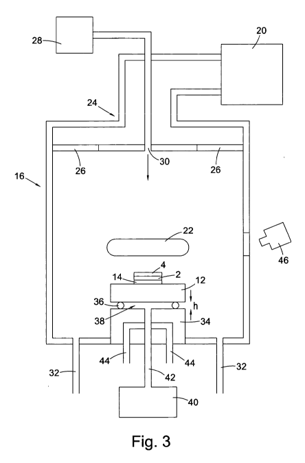
Figure 3 shows an example of a microwave plasma reactor comprising a
temperature
monitoring system and substrate temperature control system. The microwave
plasma
reactor comprises the following basic components: a plasma chamber 16; a
substrate
CA 02858965 2015-05-05
holder 18; a substrate configuration 2, 12, 14 as previous illustrated in
Figure 2 on
which CVD synthetic diamond material 4 is grown; a microwave generator 20 for
forming a plasma 22 within the plasma chamber 16; a microwave coupling
configuration 24 for feeding microwaves from the microwave generator 20 into
the
plasma chamber 16 via dielectric windows 26; and a gas flow system comprising
source gases 28, one or more gas inlets 30, and one or more gas outlets 32 for
feeding
process gases into the plasma chamber 16 and removing them therefrom.
The plasma chamber is configured to form a resonance cavity supporting a
standing
microwave in use. According to one configuration the plasma chamber is
configured
to support a TMoin standing microwave in use, e.g. a TMon mode. The
operational
frequency may be in a range 400 to 500 MHz, 800 to 1000 MHz, or 2300 to 2600
MHz. Source gases including a carbon source and molecular hydrogen are fed
into
the plasma reactor vessel and can be activated by the standing microwave field
to
form a plasma in high electric field regions. The substrate configuration is
provided
in close proximity to the plasma such that reactive carbon containing radicals
can
diffuse from the plasma to the substrate and be deposited thereon. Atomic
hydrogen
can also diffuse from the plasma to the substrate and selectively etch off non-
diamond
carbon from the substrate such that diamond growth can occur.
The support substrate 12 is spaced apart from a substrate holder 34 by spacer
wires or
spacer pads 36 to define a gas gap 38 between a supporting surface of the
substrate
holder 34 and a rear surface of the support substrate 12. The height h of the
gas gap
may be in the range 25 p.m to 2000 pri, 50 pm to 1000 pm, or 100 1-1.111 to
750 pm
depending on the specific synthesis conditions. Such gas gaps can be used with
a
support substrate having a diameter of 120 mm for example. For high
temperature
diamond synthesis processes a gas gap height in the range 500 in to 750 pm or
600
pm to 650 p.m has been found to be preferred. This contrasts with lower
temperature
diamond synthesis processes in which a gas gap height in the range 100 pm to
300
p.m or 150 m to 250 p.m is preferred. Furthermore a gas supply system 40 is
coupled
to the gas gap 38 via a supply pipe 42 which extends from the gas supply
system 40
through the substrate holder 34 and is configured to supply gas into the gas
gap 38
26
CA 02858965 2015-05-05
through one or more outlets in the supporting surface of the substrate holder
34. A
coolant liquid supply system 44 is also provided for cooling the substrate
holder 34.
It should also be noted that while the microwave plasma reactor illustrated in
Figure 5
has a separate substrate holder 34 disposed in the plasma chamber, the
substrate
holder may be formed by the base of the plasma chamber 16. The use of the term
"substrate holder" is intended to cover such variations. Furthermore, the
substrate
holder may comprise a flat supporting surface which is the same diameter (as
illustrated) or larger than the support substrate 12. For example, the
substrate holder
may form a large flat surface, formed by the chamber base or a separate
component
disposed over the chamber base, and the substrate may be carefully positioned
on a
central region of the flat supporting surface. In one arrangement, the flat
supporting
surface may have further elements, for example projections or grooves, to
align, and
optionally hold, the support substrate. Alternatively, no such additional
elements may
be provided such that the substrate holder merely provides a flat supporting
surface
over which the support substrate is disposed.
The coolant liquid supply system 44 provides a rough basic cooling to the
substrate
holder 34. However, this system has been found to be insufficiently precise
for the
fine temperature control of the substrate which is considered to be required
by the
present inventors in order to obtain uniform nitrogen uptake in CVD synthetic
diamond material grown over large support substrates. Accordingly, the gas
supply
system 40, 42 is provided in order to allow more precise control of the
support
substrate temperature. The gas supply system 40, 42 may be configured to
inject at
least two gases having different thermal conductivities into the gas gap below
the
support substrate 12 and vary a ratio of the at least two gases in order to
control the
temperature of the support substrate on the substrate holder. For example, the
gas
supply system may utilize a mixture of a light gas such as hydrogen and a
heavy gas
such as argon which is less thermally conductive. Advantageously, the gases
used to
control the temperature of the substrate are ones which are also utilized in
the main
process chemistry so that additional gas sources are not required. If an edge
temperature of the support substrate is too high relative to a central region
of the
support substrate, the proportion of heavy gas relative to light gas can be
increased to
reduce the thermal conductivity of the gas under a central region of the
support
27
CA 02858965 2015-05-05
substrate, thus causing the central region of the support substrate to heat up
relative to
the edge of the support substrate. Conversely, if the edge temperature of the
support
substrate is too low relative to the central region of the support substrate,
the
proportion of light gas relative to heavy gas can be increased to increase the
thermal
conductivity of the gas under a central region of the support substrate, thus
causing
the central region of the support substrate to cool down relative to the edge
of the
support substrate. The absolute temperature of the support substrate as well
as the
relative temperature of different regions of the support substrate can also be
controlled
by varying gas flow and gas composition within the gas gap under the support
substrate.
The spacer wires 36 may be configured to define a central gas gap cavity under
the
substrate so that the gas pools in the central gas gap cavity. The spacer
wires may
each be arcuate in shape and configured into a ring with gaps between which
the gas
can flow. The spacer elements may be electrically conductive and/or may be
fixed in
place with an electrically conductive adhesive such as Silver DAGTM which has
been
found to be useful in ensuring a good electrical contact between the spacer
elements
and the substrate holder. This aids in preventing the problem of arcing under
the
support substrate which can detrimentally affect temperature control.
The microwave plasma reactor further comprises one or more temperature
measurement devices 46 configured to take at least two temperature
measurements,
including one or more measurements in a central region of the support
substrate and
one or more measurements in a peripheral region of the support substrate. The
temperature measurements may be taken simultaneously or within a short time
interval of each other and the substrate temperature control system may be
used to
correct any temperature variations. The temperature measurement device may
comprise a pyrometer 46 as illustrated in Figure 3. Two pyrometers may be
provided,
one to take the central temperature measurements and one to take the
peripheral
temperature measurements. Alternatively, a plurality of thermocouples can be
embedded into the substrate. That said, embedding thermocouples has been found
to
be difficult and can be unreliable. As such, a plurality of pyrometry
measurements is
considered to be the better solution. In this regard, pyrometric measurements
may
focus on the temperature of the growing CVD synthetic diamond material.
However,
28
CA 02858965 2015-05-05
as the material is in good thermal contact with the underlying support
substrate then
the temperature of the diamond material will be approximately the same as the
temperature of the underlying support substrate. For single crystal CVD
synthetic
diamond growth in which a plurality of single crystal diamond substrates are
provided
on the support substrate, the temperature measurements may thus be taken
between
the growing CVD single crystals.
Even when utilizing arrangements such as those described above, a number of
problems may still exist, although these may be substantially alleviated by
the
previously described arrangements. For example, in some instances there may
still
be issues of non-uniform CVD synthetic diamond growth and non-uniform uptake
of
nitrogen across the support substrate area, particularly when growing a
plurality of
single crystal diamond crystals in a single growth run on a plurality of
single crystal
diamond substrates adhered to a support substrate over a relatively large area
(e.g. 80
mm diameter or more). This is particularly problematic as there is an on going
need
to increase the area over which high quality, uniform CVD synthetic diamond
can be
grown. Furthermore, these problems tend to be exacerbated when the support
substrates are reused in subsequent growth runs. This is particularly
problematic for
refractory metal substrates which are expensive and reuse is desirable in an
economically competitive industrial process.
It has been surprisingly found that the aforementioned problems are a result
of small
variations in temperature across the top surface of the support substrate
caused by
very minor variations in the height of the gas gap under the support
substrate. In
particular, the present inventors found that although the cylindrical
refractory metal
support substrates provided by their supplier have nominally planar front and
rear
surfaces, these surfaces are not sufficiently flat. Minor flatness variations
in a rear
surface of the support substrate result in minor variations in the height of
the gas gap
and it has been found that this results in differential cooling across the
support
substrate.
While the previously described arrangements can control variations in
temperature
which are circumferentially symmetric, it can be more difficult to control
temperature
variations which are not circumferentially symmetric such as those caused by
29
CA 02858965 2015-05-05
variations in the gas gap height. For example, refractory metal support
substrates tend
to sag and buckle during use (despite being a long way from their melting
point).
Uniform sag mainly modifies the edge to centre temperature profile which can
be
controlled as previously described. However, buckling introduces non-
uniformities in
the temperature of the support substrate which are not symmetric. Typical
buckling
magnitudes can be greater than 20 micron (peak to valley).
In order to solve this problem, the present inventors found that it is
advantageous to
ensure that the height h of the gas gap varies by no more than 200 m, 150 m,
100
pm, 80 pm, 60 m, 40 pm, 20 lam, 10 pm, or 5 pm. This may be achieved, for
example, by further processing the rear surface of support substrates provided
by
suppliers to have a very precisely defined profile which is complementary to
the
profile of the supporting surface of the substrate holder. For example, if the
supporting surface of the substrate holder is flat, then the rear surface of
the support
substrate should be processed to ensure that it is very precisely flat.
Accordingly, control of rear surface support substrate shape by mechanical
means
(preferably uniform, non-directional processing, e.g. lapping rather than
grinding) has
been found to be advantageous. Furthermore, the supporting surface of the
substrate
holder may also be processed to have a precisely defined profile which is
complementary to the rear surface of the substrate. Most conveniently this is
flat,
although other shapes can be used so long as the profile of the supporting
surface of
the substrate holder and the rear surface of the support substrate are
complementary
so as to maintain a very precisely defined gas gap height. Furthermore, it is
possible
to intentionally profile at least a portion of the supporting surface of the
substrate
holder or the rear surface of the support substrate to provide a controlled
variation in
the height of the gas gap, for example to have a smaller gas gap around the
periphery
of the support substrate to preferentially cool the peripheral region and/or
to provide
electric field modifying structures. Accordingly, the height h of the gas gap
may vary
by no more than 200 pm, 150 pm 100 pm, 80 m, 60 m, 40 ?Am, 20 pm, 10 }Am, or
5
m across at least a central region of the support substrate having a centred
diameter
equal to or greater than 60%, 70%, 80%, 90%, 95%, or 99% of a total diameter
of the
support substrate. Furthermore, the gas gap may have a central region with a
first gas
CA 02858965 2015-05-05
gap height and a peripheral region with a second gas gap height, the first gas
gap
height being larger than the second gas gap height.
The aforementioned discussion also explains why problems of non-uniform CVD
synthetic diamond growth and nitrogen uptake are exacerbated by re-use of
support
substrates. The substrate can buckle during a CVD synthetic diamond growth run
and
therefore lose flatness. As such, it has been found to be advantageous to re-
process
the support substrate between uses to regain the desired surface profile. As
the
thickness of the substrate will be reduced by such reprocessing, the substrate
holder
height may be varied to ensure that in subsequent growth runs the growth
surface of
the substrate remains at an optimum height.
Similarly, the supporting surface of the substrate holder may also be re-
processed
between growth runs to maintain the desired profile, although it has been
found that
buckling of this surface is less of a problem than variations forming in the
support
substrate. To enable the supporting surface of the substrate holder to be
readily re-
processed it is desirable to configure the chamber design such that the
substrate holder
can readily be removable, measured to determine flatness of the supporting
surface,
re-processed if necessary to maintain supporting surface flatness, and
replaced in the
plasma chamber.
In light of the above, one method for reusing the same support substrate for a
number
of synthetic diamond growth runs involves adjusting a height of the support
substrate
within the reactor, when necessary, between synthetic diamond growth runs to
account for material removed from the support substrate and/or substrate
holder by re-
processing and maintain a substantially constant height of the growth surface
during
subsequent synthetic diamond growth runs. The height of the growth surface may
be
maintained within 2 mm, 1 mm, 0.8 mm, 0.5 mm, 0.3 mm, or 0.2 mm of a target
height for the growth surface of the support substrate within the reactor.
This method
may be used to extend the life of support substrates which get reprocessed
between
runs, and therefore become thinner, while maintaining the growth surface at an
optimum height for CVD synthetic diamond growth within the reactor as
previously
discussed. The height of the growth surface may be adjusted by providing a
substrate
holder which is adjustable in height. Alternatively, if a fixed height
substrate holder
31
CA 02858965 2015-05-05
is used, once the support substrate thickness has gone below a thickness
tolerance
band as defined numerically above, the substrate holder can be changed to one
with a
step matching the diameter of the support substrate to take the growth surface
height
back into its tolerance band. Alternatively, an adjustable height substrate
holder may
be provided.
In light of the above, it has been found that the support substrate should be
processed
to have surfaces with a very high degree of flatness in order to avoid
temperature
variations leading to non-uniform nitrogen uptake during CVD synthetic diamond
growth. Such a support substrate may be formed from a refractory metal
selected
from, for example, one of molybdenum, tungsten, niobium, or alloys thereof.
According to embodiments of the present invention the flatness variation of
the front
and rear surfaces of the support substrate may be as low as possible. For
example, the
flatness variation of the surfaces may be no more than 75 jim, 50 p.m, 40 inn,
30 inn,
20 jim, 10 gm, 5 ptm, or 1 Kn. Of course, while no flatness variations would
be ideal,
some very minor variations will still usually exist depending on the limits of
the
surface processing techniques used to remove flatness variations and the
processing
time required to achieve a better flatness which will have cost implications
in an
industrial process. Accordingly, a lower limit for the flatness variations of
0.001 jim
or 0.01 pm may be applied.
The support substrate may have a diameter selected to be in the range: 165 mm
to 415
mm, 185 mm to 375 mm, 205 mm to 375 mm, 205 mm to 330 mm, or 240 mm to 330
mm for a microwave frequency fin the range 400 to 500 MHz; 80 mm to 200 mm, 90
mm to 180 mm, 100 mm to 180 mm, 100 mm to 160, or 115 mm to 160 mm for a
microwave frequency fin the range 800 to 1000 MHz; or 30 mm to 75 mm, 33 mm to
65 mm, 37 mm to 65 mm, 37 mm to 58 mm, or 42 mm to 58 mm for a microwave
frequency f in the range 2300 to 2600 MHz. Utilizing embodiments of the
present
invention CVD synthetic diamond material can be successfully grown over
support
substrates falling within these ranges while retaining uniform growth and
nitrogen
uptake. It should be noted that by "cylindrical disc", we also intend to
include discs
which are approximately cylindrical, e.g. having a cross section within a
circularity of
32
CA 02858965 2015-05-05
mm, 5 mm, or 1 mm of a mean circumference. We also intend to include edge
modifications such as chamfered edges and grooves as well as cutting errors.
Optionally, for a microwave plasma reactor with an operating frequency of 400
to 500
MHz, the cylindrical disc may have a depth in a range 10mm to 30 mm or 15 mm
to
25 mm. Alternatively, for a microwave plasma reactor with an operating
frequency in
the range 800 to 1000 MHz, the cylindrical disc may have a depth in a range 5
mm to
mm or 7 mm to 13 mm. Alternatively still, for a microwave plasma reactor with
an operating frequency of 2300 to 2600 MHz, the cylindrical disc may have a
depth in
a range 2.0 mm to 5.5 mm or 2.5 mm to 4.5 mm. The depth of the support
substrate
has been found to be important as the CVD synthetic diamond growth process is
very
sensitive to the height of the growth surface. Furthermore, the depth of the
substrate
should be sufficiently large to function as an effective heat sink.
For single crystal diamond growth where single crystal diamond substrates are
mounted on the refractory metal substrate prior to deposition, a surface
roughness of
100 nm to 500 nm may be provided prior to attachment of the single crystal
substrates
and subsequent CVD growth thereon. The surface roughness, flatness and
temperature of an underlying metallic substrate on which single crystal
diamond
substrates are mounted is important, despite the fact that the single crystal
CVD
synthetic diamond material grows on the single crystal diamond substrates
rather than
directly onto the underlying metallic substrate which supports the single
crystal
diamond substrates. This is because during single crystal diamond growth,
polycrystalline diamond material grows over the underlying supporting
substrate
between the single crystals. If this polycrystalline diamond material
delaminates
during CVD synthetic diamond growth then the growth run can be disrupted.
Furthermore, if this polycrystalline diamond material cracks on cooling this
can lead
to cracking of the single crystal diamond material embedded therein. As such,
issues
relating to growth of polycrystalline wafers can also apply to growth of
single crystal
material. In this regard, when we talk about a support substrate and a support
substrate growth surface in the context of the present invention we mean the
underlying substrate rather than single crystal substrates which are mounted
thereon
for single crystal CVD synthetic diamond growth. This underlying support
substrate
is sometimes known as a substrate carrier because it carriers further single
crystal
33
CA 02858965 2015-05-05
diamond substrates thereon. Furthermore, when we talk about the temperature of
the
growth surface of the support substrate we mean the temperature of the growth
surface of the refractory metal substrate rather than the temperature of the
growth
surface of the single crystal diamond substrates (although these temperatures
may be
approximately the same if good thermal contact between the two is achieved
using a
braze join as described herein).
Typically, the refractory metal discs are first lapped on a cast iron wheel
using
diamond grit suspended in a lapping fluid. In general, the lapping process is
used for
bulk material removal and also to achieve the required flatness for the given
process.
There are a few processes where the as-lapped surface is used. A typical Ra
value for
the lapped finish is 100 nm to 500 nm. However, the lapped surface may then be
further processed as required using, for example, a grinding/polishing machine
and
using a finer grit to obtain a lower surface roughness value. Prior to CVD
synthetic
diamond growth, the refractory metal support substrates may be cleaned to
ensure all
contamination from the lapping process has been removed.
A substrate configuration as described above has been found to be advantageous
for
use in a method of manufacturing CVD synthetic diamond material via chemical
vapour deposition, particularly in methods which utilize a microwave plasma
reactor.
However, in principle the substrate configuration could also be used in other
types of
CVD diamond reactor. Temperature variations across the support substrate can
be
controlled to be less than 50 C, 40 C, 30 C, 20 C, 10 C, or 5 C. Furthermore,
temperature variations across a single crystal diamond substrate can be
controlled to
be less than 50 C, 40 C, 30 C, 20 C, 10 C, or 5 C.
Embodiments of the synthesis method as described herein thus combine effective
thermal management in combination with a selected growth chemistry in order to
fabricate more uniform single crystal CVD synthetic diamond material using a
high
nitrogen / high substrate temperature growth process. The method comprises:
forming a CVD synthesis atmosphere comprising hydrogen, a carbon source
gas, a nitrogen source gas, and optionally an oxygen source gas, wherein the
CVD
synthesis atmosphere comprises an atomic concentration of nitrogen relative to
a total
gas composition in a range 0.1% to 3%, 0.1% to 2%, 0.1% to 1%, or 0.2% to
0.8%;
34
CA 02858965 2015-05-05
growing single crystal CVD diamond material on a single crystal diamond
substrate mounted on a support substrate; and
controlling the temperature of the support substrate such that temperature
variations across the support substrate at any given point in the growth
process are
less than 50 C, 40 C, 30 C, 20 C, 10 C, or 5 C of a target temperature value,
temperature variations throughout the growth run are less then 50 C, 40 C, 30
C,
20 C, 10 C, or 5 C of the target temperature value, and the target temperature
value
lies in a range 1000 C to 1400 C,
wherein the CVD synthesis atmosphere comprises at least one of:
an atomic concentration of carbon relative to the total gas composition in a
range 0.1% to 2.0%, 0.3% to 1.7%, 0.5% to 1.5%, 0.7% to 1.3%, or 0.8% to 1.2%;
and
an atomic concentration of oxygen relative to the total gas composition in a
range 5% to 40%, 10% to 30%, 10% to 25%, or 15% to 20%.
Using the previously described configurations, embodiments of the present
invention
may thus provide the following features:
(i) Effective thermal management using, for example, a high-temperature
braze to adhere the single crystal diamond substrates to a support substrate,
a well
processed refractory metal support substrate, and suitable temperature
monitoring and
control systems. This results in more uniform temperature gradients across
each
single crystal CVD synthetic diamond and across a plurality of single crystal
CVD
synthetic diamond crystals mounted on the support substrate. The high
temperature
braze mounting method provides an effective, simple, and cost-effective method
of
providing good thermal contact between the growing single crystal CVD
synthetic
diamond material and the support substrate.
(ii) A modified high nitrogen / high substrate temperature synthesis chemistry
using either of: (a) addition of high oxygen concentrations into the gas phase
(for
example, introduced as 02, CO2 or CO); or (b) lowering carbon source gas
concentration (for example, introduced as CH4. Both of these modifications can
inhibit non-uniform dopant/impurity uptake.
By providing the combination of a modified thermal management configuration
and a
modified synthesis chemistry it is possible to achieve a combination of
reduced
CA 02858965 2015-05-05
differential impurity uptake due to growth steps and reduced differential
impurity
uptake due to temperature variations. By achieving such a combination of
features it
has been found to be possible to synthesise single crystal CVD diamond
material
having the following features:
(i) High and uniform total nitrogen defect distributions.
(ii) High and uniform distributions of N.
(iii) High and uniform distributions of NV.
(iv) No striations.
(v) Product uniformity over a single CVD synthetic diamond stone, over a
plurality of CVD synthetic diamond stones grown within a single
growth run, and from growth run to growth run.
The resultant single crystal CVD synthetic diamond material comprises:
a total as-grown nitrogen concentration equal to or greater than 5 ppm, 7 ppm,
ppm, 15 ppm, 20 ppm, 30 ppm, 50 ppm, 75 ppm, 100 ppm, 150 ppm, 200 ppm, or
300 ppm, and
a uniform distribution of defects, wherein said uniform distribution of
defects
is defined by the following characteristic:
(i) the total nitrogen concentration, when mapped by secondary ion mass
spectrometry (SIMS) over an area equal to or greater than 50 x 50 ptm using an
analysis area of 10 jim or less, possesses a point-to-point variation of less
than 30%,
25%, 20%, 15%, 10%, 5%, 3%, or 1% of an average total nitrogen concentration
value, or when mapped by SIMS over an area equal to or greater than 200 x 200
gm
using an analysis area of 60 pm or less, possesses a point-to-point variation
of less
than 30%, 25%, 20%, 15%, 10%, 5%, 3%, or 1% of an average total nitrogen
concentration value; and optionally one or more of the following
characteristics:
(ii) an as-grown nitrogen-vacancy defect (NV) concentration equal to or
greater than 50 ppb as measured using 77K UV-visible absorption measurements,
wherein the nitrogen-vacancy defects are uniformly distributed through the
synthetic
single crystal CVD diamond material such that, when excited using a 514 nm
laser
excitation source of spot size equal to or less than10 pm at room temperature
using a
50 mW continuous wave laser, and mapped over an area equal to or greater than
50 x
50 pm with a data interval less than 10 vim, there is a low point-to-point
variation
36
CA 02858965 2015-05-05
wherein the intensity ratio of nitrogen vacancy photoluminescence peaks
between
regions of high photoluminescent intensity and regions of low photoluminescent
intensity is less than 2.0, 1.8, 1.6, 1.4, or 1.2 for either the 575 nm
photoluminescent
peak (NV ) or the 637 nm photoluminescent peak (NV);
(iii) an as-grown nitrogen-vacancy defect (NV) concentration equal to or
greater than 50 ppb as measured using 77K UV-visible absorption measurements,
wherein, when excited using a 514 nm excitation source of spot size equal to
or less
than 10 1.im at 77K using a 50 mW continuous wave laser, gives an intensity at
575
nm corresponding to NV greater than 120, 140, 160, or 180 times a Raman
intensity
at 552.4 nm, and/or an intensity at 637 nm corresponding to NV- greater than
200, 220,
240, or 260 times the Raman intensity at 552.4 nm;
(iv) a single substitutional nitrogen defect (Na) concentration equal to or
greater than 5 ppm, wherein the single substitutional nitrogen defects are
uniformly
distributed through the synthetic single crystal CVD diamond material such
that by
using a 1344 cm-1 infrared absorption feature and sampling an area greater
than an
area of 0.5 mm2, the variation is lower than 80%, 60%, 40%, 20%, or 10%, as
deduced by dividing the standard deviation by the mean value;
(v) a variation in red luminescence intensity, as defined by a standard
deviation divided by a mean value, is less than 15%, 10%, 8%, 6%, or 4%;
(vi) a mean standard deviation in neutral single substitutional nitrogen
concentration of less than 80%, 60%, 40%, 20%, or 10%; and
(vii) a colour intensity as measured using a histogram from a microscopy
image with a mean gray value of greater than 50, wherein the colour intensity
is
uniform through the single crystal CVD synthetic diamond material such that
the
variation in gray colour, as characterised by the gray value standard
deviation divided
by the gray value mean, is less than 40%, 30%, 20%, 10%, or 5% (for example as
measured over volume equal to or greater than 200 x 200 x 200 Jim with a point-
to-
point variation as specified).
The single crystal CVD synthetic diamond material may comprise two, three,
four,
five, six or all seven of said characteristics.
37
CA 02858965 2015-05-05
The single substitutional nitrogen defect (Ns) concentration may be equal to
or greater
than 5 ppm, 7 ppm, 10 ppm, 15 ppm, 20 ppm, 30 ppm, 50 ppm, 75 ppm, 100 ppm,
150 ppm, 200 ppm, or 300 ppm.
The as-grown nitrogen-vacancy defect (NV-) concentration may be equal to or
greater
than 50 ppb, 75 ppb, 100 ppb, 120 ppb, 140 ppb, 160 ppb, 180 ppb, 200 ppb, 250
ppb,
300 ppb, 400 ppb, 500 ppb, 1000 ppb, or 5000 ppb.
The single crystal CVD synthetic diamond material may have a concentration of
silicon equal to or less than 1x10¹⁵ atoms cm-3. A low silicon material may be
fabricated using the CVD reactor design as described herein which does not
comprise
a quart bell-jar or large quartz windows. Such quartz components can lead to
silicon
contamination of the single crystal CVD synthetic diamond material during
growth.
The single crystal CVD synthetic diamond material may have one or more of the
following dimensional characteristics:
a longest dimensions equal to or greater than 200 um, 500 um, 1 mm, 1.5 mm,
2.0 mm, 3.0 mm, or 5.0 mm over which one or more of the previously described
characteristics hold true;
a volume equal to or greater than 0.01 mm3, 0.05 mm3, 0.1 mm3, 0.5 mm3, 1.0
mm3, 3.0 mm3, 6.0 mm3, 9.0 mm3, or 15.0 mm3 though which one or more of the
previously described characteristics hold true;
a layer thickness less than 200 m, 100 um, 50 pm, 20 um, 10 um, 5 um, 2
pun, or 1 ytm or greater than 200 pm, 500 ptm, 1 mm, 1.5 mm, 2.0 mm, 3.0 mm,
or 5.0
mm though which one or more of the previously described characteristics hold
true.
Preferably, the single crystal CVD synthetic diamond material also has a
dislocation
bundle density equal to or less than: 106 dislocations cm-2; 104 dislocations
cm-2; 3 x
103 dislocations cm-2; 103 dislocations cm-2; 102 dislocations cm-2; or 10
dislocations
cm-2 and/or a birefringence equal to or less than 5 x 10⁻⁵, 1 x 10⁻⁵, 5 x10⁻⁶,
or 1 x10⁻⁶.
Such material can be fabricating by ensuring that the single crystal
substrates are
carefully selected and processed to provide a growth surface which is
substantially
free of crystal defects prior to growth thereon.
38
CA 02858965 2015-05-05
The single crystal CVD synthetic diamond material may be as-grown material or
may
be material which is annealed and/or irradiated. The single crystal CVD
synthetic
diamond material may have one or more of the following colours: pink, yellow,
green,
orange, red, purple.
The commercial advantages of providing one or more of the aforementioned
features
include:
(i) Material which has a more uniform quantum sensing and processing
capabilities.
(ii) Material which has more uniform optical absorbance for optical
filtering applications.
(iii) Material which has more uniform wear characteristics for mechanical
applications.
(iii) Material which has more uniform colour which is suitable for post-
growth irradiation and/or annealing treatments to form high quality
coloured gemstones.
(iv) High growth rates (e.g. greater than 30 m/hr).
It should also be noted that if the CVD synthetic diamond material is
subjected to a
post¨growth annealing treatment the nitrogen defects can aggregate to form
various
types of aggregated nitrogen defects. However, a high level of uniformity in
the
nitrogen distribution is retained such that the colour of the material remains
uniform
and little or no striation features are visible under photoluminescent viewing
conditions.
As well as other factors such as reduced metal impurities etc, the high
uniformity of
standard (i.e. lower nitrogen, lower temperature) CVD synthetic diamond
material is
normally its key advantage when compared to HPHT synthetics. For example CVD
synthetics do not posses a plurality of growth sectors. One disadvantage of
the CVD
method is that it is more difficult to incorporate high levels of nitrogen
during the
growth process when compared to HPHT growth processes. Embodiments of the
present invention address this issue and achieve high levels of nitrogen
incorporation
while also achieving more uniform nitrogen incorporation when compared to HPHT
39
CA 02858965 2015-05-05
growth processes and other CVD growth processes which utilize a high nitrogen
/
high substrate temperature process.
Examples
Utilizing the previously described CVD reactor and substrate configuration,
single
crystal CVD diamond material has been grown under high nitrogen / high
substrate
temperature conditions using various concentration of oxygen containing source
gas
and various concentrations of carbon source gas in the CVD synthesis
atmosphere.
=
Figure 4(a) is a DiamondViewTM image of a single crystal CVD synthetic diamond
material grown under high nitrogen / high substrate temperature conditions
showing
clearly visible striations. In this example the CVD synthesis atmosphere was
formed
using the following gas flow rate: 3000 sccm H2; 0 SCCM CO2; 165 sccm Cl-I4;
and 4.0
sccm pure N2 (1254 ppm). These flow rates correspond to the following atomic
concentrations: 97.5% H; 2.4% C; 0% 0; and 0.1% N.
In contrast, Figure 4(b) is a DiamondViewTm image of a single crystal CVD
synthetic
diamond material grown under high nitrogen / high substrate temperature /
oxygen
conditions showing substantially no visible striations. In this example the
CVD
synthesis atmosphere was formed using the following gas flow rate: 1000 sccm
H2;
500 sccm CO2; 530 sccm CH4; and 3 sccm N2. These flow rates correspond to the
following atomic concentrations: 67% H; 16.7% C; 16.2% 0; an 0.1% N.
Figure 5 is a DiamondViewTM image of a single crystal CVD synthetic diamond
material comprising two layers including a first layer showing clearly visible
striations which was grown using a CVD synthesis atmosphere as described above
in
relation to Figure 4(a) and a second layer showing substantially no visible
striations
which was grown using a CVD synthesis atmosphere as described above in
relation to
Figure 4(b).
Based on analysis of the DiamondViewTM image using the freeware ImageJ program
(http://rsbweb.nih.gov/ij/), it is possible to deduce a histogram of colour
values for-an
image of a diamond sample, in order to ascertain its luminescence uniformity.
The
CA 02858965 2015-05-05
sample illustrated in Figure 5 was analysed in such a manner (the {100}
surface
parallel to growth - alternatively, two {100} perpendicular surfaces can be
analysed
and the image with poorest uniformity can be taken as the surface of study). A
DiamondView image was taken so that no region of the sample image was
saturated,
the aperture and field stop settings were set to 100%, the gain value was set
to 0.00
dB (i.e. minimising noise), and the gamma enhancement setting was set to 'off
(i.e. a
linear gamma curve). The image was loaded into ImageJ. The first stage of the
analysis involved splitting the red, green and blue components of the image by
selecting the 'Split Channels' command from the 'Color' submenu under the
'Image
menu'. As the predominant colour of luminescence was red (owing to the fact
that
NV centers contributed most to the luminescence and these centres luminesce
red/orange), it was considered most sensible to analyse the red image
component and
to reject the green and blue components. Next, from the red component, a
selected
rectangle was taken from each CVD layer, avoiding the sample surface, the
substrate
and any twinned or included regions that could influence the measurement. Note
that
this rectangle should be larger than 0.3 mm2 or preferably larger than 0.6 mm2
or
more preferably larger than 1.0 mm2. Clicking 'Analyse' and then 'Histogram'
revealed the following histogram and the statistical parameters:
Area (mm2) Mean S.D. Min Max Mode S.D. /mean (%)
HT/HN layer 1 1.7+/-0.2 97.569 18.117 48 164 94 18.6
HT/HN/O layer 2 1.7+7-0.2 122.712 5.768 100 154 125 4.7
One can deduce the following from the above data: (i) the areas measured are
very
similar and both are representative of the sample face; (ii) the mean value
for the
HT/HN/O layer is higher than that of the HT/HN layer suggesting that 0 has the
effect of increasing the strength of red luminescence (i.e. higher NV
luminescence
intensity); (iii) most pertinent to this invention, the standard deviation for
the
HT/HN/O layer is much smaller than for the HT/HN layer, as expected from
Figure 7;
(iv) there is a far smaller spread in Min and Max values for the HT/HN/O layer
than
for the HT/HN layer, consistent with (iii); and (v) the mode of the HT/HN/O
layer is
higher than for the HT/HN layer, consistent with (ii).
41
CA 02858965 2015-05-05
From this analysis, we can say that improved luminescence uniformity by
employing
either a heavy 0-doped chemistry or by reducing methane is characterised by a
variation in red luminescence intensity, as defined by the standard deviation
divided
by the mean in the manner described above, of less than 15% or preferably less
than
10% or more preferably less than 8% or more preferably less than 6% or more
preferably less than 4%.
Figure 6 is a DiamondViewTM image of a single crystal CVD synthetic diamond
material comprising two layers including a first layer showing clearly visible
striations which was grown under high nitrogen / high substrate temperature
conditions and a second layer showing substantially no visible striations
which was
formed by reducing the concentration of methane in the synthesis atmosphere.
For
the first layer the CVD synthesis atmosphere was formed using the following
gas flow
rate: 3000 sccm H2; 20 sccm Ar; 165 sccm CH4; and 4 sccm N2. These flow rates
correspond to the following atomic concentrations: 2.4% C; and 0.1% N. For the
second layer the CVD synthesis atmosphere was formed using the following gas
flow
rate: 3000 sccm H2; 20 sccm Ar; 45 sccm CH4; and 4 sccm N2. These flow rates
correspond to the following atomic concentrations: 0.7% C; and 0.1% N.
Figure 7 shows photoluminescence (PL) maps for the two layer single crystal
CVD
synthetic diamond material shown in Figure 5. These photoluminescence maps
were
taken using 50mW continuous-wave laser excitation at 514 nm (Ar laser) with
the
sample held at room temperature. A laser spot size of less than 10 wn
diameter, more
preferably less than 5 p.m diameter, is utilized. A 600 lines/mm grating was
used,
giving a spectral resolution of about 0.1 nm. The grating was positioned so
that
spectral data from 550-650 nm could be collected. The laser was raster-scanned
over
a 250 um x 250 um region of a polished surface of the sample that was parallel
to the
<100> growth direction. In practice, a raster scan > 50 pm x 50 um would be
sufficient. The step increment was 5 gm. In order to calculate the line
intensities at
room temperature, the following method was applied. First, each peak was
baselined
using a polynomial fit to the baseline region. The Raman peak at 552.4 nm was
sharp,
and therefore a baseline window of 551-554 nm was sufficient. The 575 and 637
nm
features were far broader, and therefore baselining windows of 570-582 nm (575
rim
42
CA 02858965 2015-05-05
peak) and 630-645 run (637 nm peak) were required. Then, before analysis of
each
peak, the spectrum was converted from nm on the x-scale to eV. Then, for each
peak,
an integrated area was deduced by fitting to each of the peaks using a mixed
Gaussian/Lorentzian non-linear least squares algorithm. The resulting peak
area is in
eV counts per second (cps). This procedure was followed for the diamond Raman
at
552.4 nm, the 575 nm feature and the 637 nm feature. This was performed for
the
regions of lowest and highest 575 and 637 nm line intensity in each of the
layers.
Normalised 535 and 637 nm line area values were calculated by dividing the 575
and
637 areas by the area of the diamond Raman line. The values are shown in the
following table:
Layer 1 (HT/HN) Layer 2 (HT/HN/O)
lowest highest lowest highest
Raman area (cps.eV) 17.77 13.45 18.79 17.23
575 nm area (cps.eV) 187.96 307.65 419.09 636.31
637 nm area (cps.eV) 493.69 838.44 1051.1 1721.3
575 nm /R ratio 10.99 22.87 22.30 36.93
637 nm / R ratio 28.85 62.34 55.93 99.88
highest/lowest (Raman) 1.27 1.09
highest/lowest (575 nm) 2.08 1.66
highest/lowest (637 nm) 2.16 1.79
From this table it is clear that the integrated area of the diamond Raman
feature varies
by approximately 1.3x between regions of low PL intensity and high PL
intensity in
the standard HT/FIN-grown layer, but only by approximately 1.1x in the HT/HN/O-
grown layer. We note that these values are the minimum and maximum Raman
values
measured over the sample surface - the region of lowest Raman intensity was
observed to correspond directly to the region of highest 575 and 637 nm PL,
and vice
versa. Therefore, certain embodiments of the present invention can be
demonstrated
if integrated area ratio of the diamond Raman feature over the sample area
measured
in this manner is <1.25 or preferably <1.20 or more preferably <1.15 or more
preferably <1.10 or more preferably <1.05.
43
CA 02858965 2015-05-05
From this table it is also clear that for both the 575 and 637 nm features in
the
HT/HN-grown layer there is a variation of greater than 2x between regions of
low
intensity and regions of high intensity, whilst in the HT/HN/O-grown layer,
the
variation is less than 2x. Therefore, certain embodiments of the present
invention can
be demonstrated if the normalised 575 or 637 luminescence intensity ratio
between
regions of high PL intensity and regions of low PL intensity are <2 or
preferably <1.8
or more preferably <1.6 or more preferably <1.4 or more preferably <1.2.
It is also noted that the PL line intensity values are greater for layer 2
than for layer 1.
Although there is some overlap, we can say that, for room temperature PL
measurements, 575 nm /R values greater than 30 and/or 637 nm /R values greater
than
70 characterise certain embodiments of the present invention invention.
PL at 77K (liquid nitrogen temperature) can also be used to further
investigate the 575
and 637 nm lines. On the same sample, PL was performed at 77K using the same
setup and 514 nm excitation. At 77K both the 575 and 637 nm PL lines sharpen
considerably and increase in intensity. The sample was cooled using a standard
cryostat and sufficient delay was allowed for the sample to reach 77K (the
temperature was measured close to the sample using a thermocouple). Then the
spectrum between 520 and 850 nm was taken. In order to calculate the line
intensities
at 77K, the following method was applied. First, each peak was baselined using
a
polynomial fit to the baseline region. As the Raman and PL peaks were sharp
and the
baseline was close to zero, this was not problematic. Then, before analysis,
the
spectrum was converted from nm on the x-scale to eV. Then, for each peak, an
integrated area was deduced by fitting to each of the peaks using a mixed
Gaussian/Lorentzian non-linear least squares algorithm. The resulting peak
area is in
eV counts per second (cps). This was done for the diamond Raman at 552.4 nm,
the
575 nm feature and the 637 nm feature. The normalised PL line intensities for
two
spots taken on the sample, one for the HT/HN layer and the other for the
HT/HN/O
layer, are shown below:
Layer 1 (HT/FN) Layer 2 (HT/HN/O)
575 nm /R area ratio 85.90 144.66
637 nm / R area ratio 167.69 223.80
44
CA 02858965 2015-05-05
Although it is clear from that there is considerable spread in the 575 and 637
line area
ratios for layer 1, is has been noted that the values are larger for layer 2
than for layer
1. This is also observed in the DiamondView images (e.g. as shown in Figures 5
and
6). The 77K results also appear to support the room-temperature results
already
shown. Thus we can say that, for 77K PL measurements, 575 nm /R values greater
than 120 and/or 637 nm /R values greater than 200 characterise certain
embodiments
of the present invention.
As-grown NV defects such as those discussed above can straightforwardly be
distinguished from those which are at least in part formed by irradiation and
annealing
as CVD synthetic diamond material treated in such a way shows features present
in
the UV-visible, IR or PL spectra that are not present in as-grown CVD
synthetic
diamond. These include: the 594 nm feature in UV-visible absorption; the 1450
cm-1
feature in IR spectra; and features such as the 470 nm and 550.8 nm features
in PL.
Furthermore, as-grown nitrogen defects can be distinguished over implanted
nitrogen
due to: (i) the absence of implantation damage; and (ii) the nitrogen defects
are
distributed throughout the diamond material, or a layer of material grown as
described
herein, rather than in a near surface plane formed by implantation. As such,
in
accordance with the present invention nitrogen defects are distributed
uniformly when
analysed in two orthogonal planes.
Figure 8 is a microscopy image of a single crystal CVD synthetic diamond
material
comprising two layers including a first layer showing clearly visible colour
non-
uniformity which was grown under high nitrogen / high substrate temperature
conditions and a second layer showing substantially improved colour uniformity
which was formed by adding oxygen to the synthesis atmosphere. For the first
layer
the CVD synthesis atmosphere was formed using the following gas flow rate:
3000
sccm H2; 165 sccm CH4; and 40 sccm of a 10% N2: H2 mix. These flow rates
correspond to the following atomic concentrations: 2.4% C; and 0.1% N. For the
second layer the CVD synthesis atmosphere was formed using the following gas
flow
rate: 380 sccm H2; 530 sccm CI-14; 470 sccm CO2, and 10 sccm of a 10% N2: H2
mix.
These flow rates correspond to the following atomic concentrations: 20.7% C;
19.5%
0; and 0.04%N.
CA 02858965 2015-05-05
In a similar manner to the analysis of the DiamondView image (shown in Figure
5),
based on analysis of the microscopy image using the freeware ImageJ program
(http://rsbweb.nih.gov/ij/), it was possible to deduce a histogram giving the
distribution of gray values for an image of a diamond sample, in order to
ascertain its
uniformity in colour. The sample shown in Figure 8 was analysed in such a
manner
(the {100} surface parallel to growth - alternatively, two {100} perpendicular
surfaces
can be analysed and the image with poorest uniformity can be taken as the
surface of
interest). The original microscopy image was taken with the growth features in
sharp
focus using a CCD camera of more than 2 megapixels, and a magnification chosen
such that the longest length axis of the sample occupied at least 50% of the
image
width. The image acquisition conditions were taken so that the background was
saturated, but no region of the sample was saturated, and a gamma setting of
0.5, thus
ensuring good contrast and brightness. The image was loaded into ImageJ. For
analysis, the largest selection rectangle possible was taken from each CVD
layer,
avoiding the sample surface, the substrate and any twinned or included regions
that
could influence the measurement. Note that this rectangle should be larger
than 0.3
mm2 or preferably larger than 0.4 mm2 or more preferably larger than 0.5 mm2.
Clicking 'Analyse' and then 'Histogram' revealed the histogram and the
statistical
parameters:
Area (mm2) Mean S.D. Min Max Mode S.D./mean (%)
HT/HN layer 0.97 140.54 64.613 46 239 223 42.9
HT/HN/O layer 0.77 120.27 7.593 73 151 119 6.3
One can make a number of deductions from the above data: (i) although the area
measured in the HT/HN layer was greater than the area measured in the HT/HN/O
layer (the former was thicker so this was possible), both areas are of a
similar order
and encompass a reasonable area of the sample face; (ii) the mean gray value
for the
HT/HN layer is higher than that of the HT/HN/O layer suggesting that overall,
oxygen
appears to have the effect of improving colour; (iii) most pertinent to this
invention,
the standard deviation is much smaller for the HT/HN/O layer than for the
HT/HN
layer, as expected from Figure 8; (iv) there is a far greater spread in Min
and Max
gray values for the HT/HN layer than for the HT/HN/O layer, consistent with
(iii);
and (v) the mode of the HT/HN layer is higher than for the HT/HN/O layer,
consistent
46
CA 02858965 2015-05-05
with (ii). From this analysis, we can say that improved colour uniformity by
employing either a heavy 0-doped chemistry or by reducing methane is
characterised
by a variation in gray colour, as characterised by the gray value standard
deviation
divided by the gray value mean, of less than 50%, 40% 30%, 20%, 10% or 5%.
A microscope attached to a NicoletTM Magna-IR 750 Fourier-transform infrared
(FTIR) spectrometer was used in order to measure the nitrogen concentration
and the
nitrogen uniformity in the HT/HN and HT/HN/O grown layers for the sample shown
in Figure 8. Again, a {100} surface parallel to the growth direction was
studied. A
representative sample of five spots was measured for each layer. By a
representative
sample, we mean that 5 spots were measured to give as good an indication of
the
spectral characteristics of each layer, whilst avoiding the following features
which
may lead to erroneous results: (a) twinned growth; (b) the sample substrate;
and (c)
the sample surface. In practice, more spots could be measured but 5 points in
each
layer is a good lower limit. The sizes of the apertures used were 1.5 mm for
the upper
aperture and 1 mm for the lower aperture. The
spectrometer was set up for
acquisition using 512 scans between 650 and 4000 cm-I with a spectral
resolution (as
defined by the instrument settings) of 2 cm-I. Before data acquisition, a
background
spectrum was acquired and the background spectra were subtracted from the
sample
spectra. Following acquisition of the sample spectra, the IR spectrum of water
vapour
was subtracted from the sample spectra. Then, the spectra were normalised by
dividing with the spectrum of a standard type Ha natural diamond of known
thickness
to give absorption coefficient values in terms of cm-1.
It is well known (e.g. S. C. Lawson, D, Fisher et al. J. Phys.: Condens.
Matter 10
6171-6180 (1998)) that the intensity of the IR feature at 1344 cm-1 may be
used for
deducing the neutral single substitutional nitrogen concentration ([1\1M). By
fitting to
the area of the feature at 1344 cm-1 and multiplying by a factor of 14.70, [NM
values
were deduced for 5 representative points in the HT/HN layer, and for 5
representative
points in the HT/HN/O layer. The multiplication factor has been determined
previously and been found to give an accurate value for deducing [NM over a
wide
range of diamond samples. Mean and standard deviations of [NM were deduced for
each layer. The Table below shows the values that were obtained:
47
CA 02858965 2015-05-05
[Nsl (ppm) Mean [1\41 (ppm) S.D. (ppm) S.D./MEAN (%)
HT/HN point 1 13.7
HT/HN point 2 18.4
HT/HN point 3 25.1 11.4 11.2 98.0
HT/HN point 4 0.0
HT/HN point 5 0.0
HT/HN/O point 1 21.2
HT/IIN/0 point 2 21.2
HT/HN/O point 3 19.1 19.9 2.9 14.5
HT/HN/O point 4 22.8
HT/HN/O point 5 15.3
Several points can be observed from the above table: (i) the mean [N, ] is
higher for
the HT/HN/O layer than the HT/HN layer, suggesting that is likely to be of
benefit for
increasing the concentration of nitrogen within the material, which is useful
for
certain applications; And (ii) the standard deviation of Ns is significantly
greater for
the HT/HN layer than for the HT/HN/O layer, indicating greatly improved
nitrogen
uniformity in the HT/HN/O layer. To summarise, the HT/HN/O layer is
characterised
by a variation in neutral single substitutional nitrogen concentration (as
measured
over as wide an area of the sample as possible but using at least 5 spots
sampling an
area greater than an area of 0.5 mm2, using the 1344 cm-1 feature in IR
spectra) of
lower than 80% or preferably lower than 60% or more preferably lower than 40%
or
more preferably lower than 20% or more preferably lower than 10%, the
variation
deduced by dividing the standard deviation by the mean.
In addition to the above, secondary ion mass spectroscopy (SIMS) mapping may
be
performed in order to determine variations in the total nitrogen concentration
within a
sample. First, the N signal is calibrated using a reference diamond sample of
known
nitrogen concentration. Then, in order to define the analysis area, an
aperture is placed
in front of a rastered SIMS beam (which is typically 15 keV 18024). For the
purposes
of this study, a 10x10 micron aperture is used. This translates to a N
concentration
sensitivity in the order of a few parts per million (greater sensitivities may
be
employed by using larger apertures). This aperture is then mapped over the
sample
48
CA 02858965 2015-05-05
point-by-point. At each point, the beam is applied for typically 10 minutes in
order to
collect data typically 2 microns within the diamond sample, this minimising
the
contribution from atmospheric contamination. In this manner, over several
hours, a
5x5 map will allow a 50x50 micron region of the sample to be sampled.
Samples can also be treated by way of irradiation and/or annealing. For
example,
HPHT treated samples still have an Ns concentration and distribution within
the
previously discussed limits although the 50 ppb NV limit may no longer apply
as NV
defects can be at least partially annealed out of the material. Colour and
luminescence will remain uniform. Depending on the specific starting material
and
the HPHT treatment the colour of treated samples may be colourless, yellow, or
grey.
Having regard to luminescence, this will no longer tend to be a
characteristics
red/orange NV luminescence but rather a green luminescence or blue-green
luminescence. Spectroscopic features that (i) come up on annealing and (ii)
are CVD
specific include: 524.3 nm in PL, 1341 cm-I in IR; and 451/454 nm in 77K UV-
Vis
absorption. Multiple annealing and/or irradiation steps can be performed to
achieve
specific target colours. For example, a triple treatment comprising annealing,
irradiating, and annealing can be applied to a material of the present
invention. Such
a triple treatment can be used to achieve a pink colouration. Again, such
treated
samples still have an Ns concentration and distribution within the previously
discussed
limits. Uniformity in terms of colour and luminescence is also retained.
Triple-
treatment features include the above annealing-related CVD features plus a 594
nm
feature in 77K UV-vis absorption and a 1450 cm-1 feature in IR (as well as
strong
575/637 nm luminescence from NV defects).
These examples illustrate the improvements in material quality achieved by
embodiments of the present invention. However, while the invention has been
particularly shown and described with reference to preferred embodiments, it
will be
understood to those skilled in the art that various changes in form and detail
may be
made without departing from the scope of the invention as defined by the
appending
claims.
49