Note: Descriptions are shown in the official language in which they were submitted.
CA 02859079 2014-06-11
WO 2013/116018 PCT/US2013/022265
LOAD BALANCED SPLIT-PHASE MODULATION AND HARMONIC
CONTROL OF DC-DC CONVERTER PAIR/COLUMN FOR REDUCED
EMI AND SMALLER EMI FILTERS
CROSS-REFERENCE TO RELATED APPLICATION
[0001] This application claims priority to U.S. patent application Serial
No. 13/360,951,
filed January 30, 2012, which is incorporated herein in its entirety by
reference.
BACKGROUND
1. TECHNICAL FIELD
[0002] The present disclosure relates to the supply, regulation, and
conversion of power,
including the supply, regulation, conversion, and reduction of electromagnetic
interference
(EMI) for a direct current (DC) power converter for aircraft, vehicle and
telecommunications
applications.
2. DESCRIPTION OF THE RELATED ART
[0003] Most DC-DC converters and power supplies operate in isolation¨i.
e., a single-
converter circuit operates independently of other converters. For example, a
single Buck
converter, or its variation, employs only a single internal power-switching
device (referred to as
modular level N=1). Systematic, coordinated control at the system level for
multiple Buck
converters may improve the output voltage waveform over non-coordinated
control. For
example, a circuit connection topology may be provided with parallel
connections of the output
power terminals of multiple individual converter cells to organize the output
voltage waveforms
from the individual Buck converter units with a proper phase arrangement to
reduce the output-
voltage ripple. However, the state of the art is limited with respect to the
improvement of
converter input waveforms and does not include parallel connections and
coordinated operations
at the input terminals of multiple converters. Thus, known converters may not
address issues
such as electromagnetic interference (EMI) and electromagnetic compatibility
(EMC) on the
input side. As a result, known arrangements must employ large and heavy EMI
filters to
attenuate undesirable harmonics and electromagnetic interference at the
converter input ports, or
else the converters produce a significant amount of undesirable conductive and
radiated
emissions that are proportional to the load power/current level. Such large
EMI filters, which
add significant weight and bulk to the power supply, are undesirable for many
applications,
including aerospace applications.
CA 02859079 2014-06-11
WO 2013/116018 PCT/US2013/022265
SUMMARY
[0004] Many industries, such as aerospace and telecommunications, have
imposed
rigorous regulatory standards/requirements for EMI and EMC on the power
converter's input
side, where EMI is more likely to interfere with other users/equipments
sharing the same power
input bus. The regulations generally include both radiated and conducted
emissions and cover a
wide frequency range of over 30 MHz.
[0005] The present disclosure describes new systems for advanced control,
modular
configuration and optimal cross-module modulation of multiple converter cells.
The circuit
topology of this new scheme may include parallel connections at the input
power terminals of
each individual converter cell, but may have no direct parallel connections in
the output side
(i.e., isolated outputs). Control and modulation of the multiple converter
cells may include
coordinated split-phase and/or multiple-phase modulation with an additional
load balancing
scheme or stage. Such a control and modulation scheme enables reduction of the
input
harmonics at the input port of the DC-DC power converters and enables EMI
cancellation (or
significant reduction) at the core circuit of power switching, where the EMI
noise sources are
located.
[0006] To illustrate the basic principle, the disclosure starts from a
very basic scheme
that employs two identical core circuits of DC-DC converters (modular level
N=2), but uses a
phase-angle-differential modulation of 180 electric degrees with a novel load
current balancing
configuration. The novel load current balancing design embedded together with
the load
matching or management allows the two converters to operate close to a 50%
duty cycle in most
nominal steady-state operations. As a result, the total input current to the
converters can be a
smooth DC current, rather than a square-wave pulsating current. This
simplified example shows
that the techniques of this disclosure can effectively reduce input current
pulsation, thus reducing
the rapid transient components in the input current and reducing transient
current induced EMI.
In addition, the approach of this disclosure also facilitates EMI cancellation
in the main input
current paths by a top-bottom pair layout of the PCB traces in the respective
DC-DC converters.
[0007] A more in-depth disclosure of load balanced, multiple-phase
modulation and a
modular circuit scheme for low-EMI DC-DC conversion is further discussed in
this disclosure at
a modular level N=3. Quantitative theoretical analysis, digital simulation and
initial
experimental results have shown that this can effectively and significantly
reduce input harmonic
2
CA 02859079 2014-06-11
WO 2013/116018 PCT/US2013/022265
currents and improve EMI reduction at all load conditions. Further, multiple-
phase modulation
and a modular circuit scheme for low-EMI DC-DC conversion is further disclosed
for a modular
level N = k, where k>1 and k is an integer.
[0008] In an embodiment, a power conversion circuit providing the above-
noted
advantages may include two or more direct current to direct current (DC-DC)
converters and a
load-balancing circuit portion. The converters may be configured to receive
input power from
two or more input power sources, and further configured to be modulated with
an electrical
signal phase differential relative to one another. The load balancing circuit
portion may be
coupled with respective outputs of the DC-DC converters and configured to
balance the
respective loads on the DC-DC converters with each other.
[0009] In an embodiment, the power conversion circuit may further include
an EMI filter
coupled with the power sources and with the input of the DC-DC converters. The
EMI filter
may include two, or more, channels. Each channel can be configured to receive
input power
through a respective power bus.
[0010] Another embodiment of a power conversion circuit providing the
above-noted
advantages may include a DC converter group comprising a plurality of DC-DC
converter cells
and parallel input power terminal connections for two or more of the
individual converter cells in
the converter group, wherein the output terminals of the individual converter
cells are isolated
from each other. The circuit may further include a multiple-phase modulation
controller coupled
with the DC converter group and a load balancing circuit portion, the load
balancing circuit
portion coupled with respective outputs of the DC-DC converters, and
configured to balance the
respective loads on the DC-DC converters with each other.
[0011] Still another embodiment of a power conversion circuit providing
the above-noted
advantages may include an electromagnetic interference (EMI) filter column
configured to be
coupled with an input power source, two or more direct current to direct
current (DC-DC)
converters coupled with the output of the EMI filter column, and a modulation
controller. The
modulation controller may be coupled with the DC-DC converters and may be
configured to
modulate the DC-DC converters with phase angle differential modulation wherein
the relative
electrical signal phase differential between two of the DC-DC converters is
inversely
proportional to the number of converters that are modulated together.
[0012] More disclosures are given in the following sections and Figures:
3
CA 02859079 2014-06-11
WO 2013/116018 PCT/US2013/022265
BRIEF DESCRIPTION OF THE DRAWINGS
[0013] Embodiments of the invention will now be described, by way of
example, with
reference to the accompanying drawings, wherein:
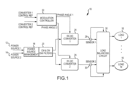
[0014] FIG. 1 is a block diagram view of an embodiment of a power
conversion circuit
including a DC converter column (dual cell) applying a load balanced, split-
phase modulation
scheme.
[0015] FIG. 2 is a block diagram view of an embodiment of a power
conversion circuit
scheme including a DC converter column (dual cell) with control compensation
for load
balancing and split-phase modulation.
[0016] FIG. 3 is a block diagram view of an embodiment of a power
conversion circuit
including a load balanced multiple cell converter column with coordinated
cross-cell control of a
split-phase modulation scheme.
[0017] FIG. 4 is a schematic and block diagram view of an exemplary
embodiment of a
multiple-phase modulation and modular circuit scheme for an aircraft cockpit
control panel
illumination and LED load application.
[0018] FIG. 5 is a schematic view of an exemplary embodiment of an
individual
converter cell.
[0019] FIGS. 6A-6C are plots illustrating theoretical input current
waveforms for
exemplary embodiments of modulation schemes for a single DC-DC converter (N=1)
with a
single switch, at duty cycles of D= 1/3, D=2/3 and D=2/3, respectively.
[0020] FIGS. 7A-7B are plots illustrating theoretical input current
waveforms for
exemplary embodiments of split-phase modulation schemes for three DC-DC
converters (N = 3),
with a single switch, at duty cycles of D= 1/3 and D=2/3, respectively.
[0021] FIGS. 8A-8B are plots illustrating theoretical input current
waveforms for
exemplary embodiments of split-phase modulation schemes for three DC-DC
converters (N = 3)
at duty cycles of D= 1/2 and D=5/6, respectively.
[0022] FIGS. 9A-9B are plots illustrating theoretical input current
frequency spectra for
exemplary embodiments of split-phase modulation schemes at a duty cycle of D=
1/2 for three
DC-DC converters (N = 3) and one DC-DC converter (N=1), respectively.
4
CA 02859079 2014-06-11
WO 2013/116018 PCT/US2013/022265
DETAILED DESCRIPTION
[0023] FIG. 1 is a block diagram view of an embodiment of a power
conversion circuit
10. The circuit 10 receives input power from a first power source 12 and a
second power source
14, and the circuit output is coupled to a plurality of loads 16. The
illustrated circuit 10 includes
a power source management portion 18, which itself includes an electromagnetic
interference
(EMI) filter 20, a modulation controller 22, two direct current to direct
current (DC-DC)
converters 24, 26, two sensors 28, 30, and a load balancing portion 32.
[0024] The power source management portion 18 of the circuit 10 is
coupled to both
input power sources 12, 14. In an embodiment, the EMI filter 20 is coupled
directly to both
input power sources 12, 14. The power source management portion 18 and the EMI
filter 20
may comprise conventional components and topologies known in the art.
[0025] The DC-DC converters 24, 26 are coupled to the output of the power
source
management portion 18 of the circuit and, in an embodiment, coupled to the
output of the EMI
filter 20. Both of the DC-DC converters 24, 26 may comprise conventional
components known
in the art and, in an embodiment, may be identical to each other. The DC-DC
converters 24, 26
may be configured to increase or decrease the voltage from their input side
(i.e., power sources
12, 14) to their output side (i.e., loads 16). In an aircraft embodiment in
which the power
management circuit 10 is used to provide power from a main aircraft power bus
to an instrument
panel, light dimming controller, or other system, the DC-DC converters 24, 26
may change
voltage from input to output. For example, the power sources 12, 14 may
provide input power at
28V, and the DC-DC converters 24, 26 may decrease the voltage to 24V for the
loads 16.
[0026] The modulation controller 22 may be coupled to both of the DC-DC
converters
24, 26 and may provide a modulation signal for each converter. In an
embodiment, the
modulation controller 22 applies a "split-phase" modulation scheme in which
the converters 24,
26 are modulated approximately 180 electrical degrees out of phase with each
other. To do so,
the modulation controller may provide separate modulation signals to the
converters that have a
relative phase differential of 180 degrees. The underlying modulation scheme
to which the
phase differential is applied may be a scheme known in the art (e.g., pulse-
width modulation).
The modulation controller 22 may adjust the modulation scheme and the phase
differential in the
respective modulation signals for the DC-DC converters 24, 26 according to
respective
CA 02859079 2014-06-11
WO 2013/116018 PCT/US2013/022265
modulation control reference signals. The respective reference signals may be
related to the
output of the converters or to a signal present at an intermediate stage of
the converters.
[0027] The load balancing portion 32 of the circuit 10 may be coupled to
the output of
the converters 24, 26 and may distribute power to loads 16 such that the load
on (i.e., the power
provided by) each of the converters 24, 26 is approximately equal. The load
balancing portion
32 may receive additional input from sensors 28, 30 indicative of respective
output
characteristics (e.g., power, voltage, current) of the converters 24, 26 and
may distribute power
accordingly. In general, the load balancing can be achieved in real time
(i.e., "on-line") by a
load managing/balancing circuit, or in an off-line load balancing/management
process, or with
both. The connection topology illustrated in Figure 1 allows multiple output
voltage levels for
different loads having different voltage ratings while balancing each output
power to be
approximately equal.
[0028] The topology of the power conversion circuit 10 can provide
advantages over
power supplies and power conversion circuits and topologies known in the art.
For example,
without limitation, by applying a split-phase modulation scheme to the
converters 24, 26 and
balancing the loads on the converters 24, 26, the circuit 10 can reduce the
input current pulsation
and EMI¨both conductive and radiated¨produced at the input. As a result, the
EMI filter 20
can then be constructed to be comparatively smaller than in known circuits,
allowing for a
smaller, lighter and less expensive circuit. Moreover, the combination of
split-phase modulation
and load balancing can permit the converters 24, 26 to operate close to a 50%
duty cycle in most
nominal steady-state operations. As a result, the input current pulsation may
be reduced further
and the power quality can be improved for loads connected to the power sources
12, 14. In a
further embodiment, the circuit 10 can be laid out in a top-bottom pair
configuration on a printed
circuit board (PCB). A top-bottom PCB layout can further reduce EMI at the
input of the circuit.
[0029] FIG. 2 is a block diagram view of another embodiment of a power
conversion
circuit 34. The illustrated power conversion circuit 34 generally includes the
same or similar
components and electrical connections as the previously illustrated circuit
10, but may provide
additional load balancing functionality. In power conversion circuit 34,
sensors 28, 30 may be
additionally electrically coupled to modulation controller 22. The modulation
controller 22 can
use the information provided by the sensors 28, 30 to adjust the modulation
signals for the DC-
DC converters 24, 26, at a small signal mode. By adjusting the modulation
signals (while still
6
CA 02859079 2014-06-11
WO 2013/116018 PCT/US2013/022265
modulating the converters, e.g., approximately 180 degrees out-of-phase with
each other), the
modulation controller 22 can further balance the respective loads on the
converters 24, 26.
[0030] The topology and control scheme described above can be extended to
a higher
number of modular level N=k, where k>1 and k is an integer. As illustrated and
discussed below,
quantitative theoretic analysis, digital simulation and initial experimental
results have shown that
this can effectively and significantly reduce the input harmonic currents and
benefit EMI
reduction at all load conditions.
[0031] The load-balanced modulation scheme illustrated in FIGS. 1-2 may
be applied to
higher modular levels (i.e., a greater number of converter cells), such as
N=3.
[0032] FIG. 3 is a block diagram view of yet another embodiment of a
power conversion
circuit 36 which generally illustrates the scalability of both of the
previously-illustrated circuits
10, 34. The circuit 36 generally includes many of the same or similar
components and electrical
connections as the previous circuits 10, 34, but with additional converter
channels. The circuit
36 includes a plurality N of DC-DC converters, with three such converters 24,
26, 38 shown.
The circuit 36 also includes a plurality N of sensors, with three such sensors
28, 30, 40, shown,
and N loads 16. The number N may be customized to suit a particular
application. Although N
loads are shown, the number of loads can be different from the number of
converter channels.
[0033] Each element in the circuit 36 can be scaled to accommodate any
number N of
DC-DC converters. Power source management portion 18 and EMI filter 20 may
each have a
channel for each DC-DC converter, each of the N DC-DC converters may have an
associated
sensor, and the load balancing circuit portion 32 may be configured to
distribute power from N
converters to the loads 16 according to input from the N sensors.
[0034] The modulation controller 22 also can be scaled to provide N
modulation
signals¨i.e., a separate modulation signal for each of the N converters 24,
26, 38. In an
embodiment including more than two such converters, the phase angle
differential between
converters may be inversely proportional or otherwise related to the number of
converters that
are modulated together. For example only, in an embodiment, the phase angle
differential 0 (in
degrees) between the first converter 24 and each other converter k may be
calculated
approximately according to equation (1) below:
7
CA 02859079 2014-06-11
WO 2013/116018 PCT/US2013/022265
ilf-0
Ok =-180 _____________________________________________________ (Eq. 1)
N j
Where k = 1,. . . , N. In such an embodiment, the relative phase angle
differentials may be
evenly distributed among the several converters, as illustrated in FIGS. 7A-7B
and 8A-8B. In
another embodiment, the relative phase angle differential between converters
may follow another
pattern or scheme.
[0035] FIG. 4 is a schematic and block diagram view of an exemplary
embodiment of a
DC-DC converter 42 that may find use in one of the systems 10, 34, 36. The
converter 42
includes an input resistance 44, and plurality of light-emitting diodes (LEDs)
46, a switch device
(transistor or MOSFET) 48 for voltage modulation, and a gate controller 50.
For ease of
illustration, not all diodes 46 are labeled. The input resistance 44 and LEDs
46 comprise the
load on the converter 42.
[0036] Under the control of the gate controller 50, the transistor 48 may
switch on and
off to modulate the load voltage of converter 42. The gate controller 50 may
apply a modulation
scheme as known in the art such as, for example only, pulse-width modulation.
Reference
signals and modulation phase information may be provided by a central
controller (e.g.,
modulation controller 22 generally illustrated in FIGS. 1-3).
[0037] The converter 42 can be one in a series of many DC-DC converters
operated in
parallel, as illustrated by DC-DC converter k+i. The converter 42 can be
configured to share a
common input current IN and a common input voltage VINT with other converters.
And as
described in conjunction with FIGS. 1-3, the converter 42 and other converters
can be
modulated according to a common scheme (e.g., split-phase modulation) to
provide a high-
quality power interface.
[0038] FIG. 5 is a schematic and block diagram view of another exemplary
embodiment
of a DC-DC power converter 52 that may find use in one of the systems 10, 34,
36. The
converter 52 is a buck converter including a switch 54, a diode 55, and an
inductor 56. The input
of the converter is coupled with a power supply 60, and the output of the
converter is coupled
with a load 62.
8
CA 02859079 2014-06-11
WO 2013/116018 PCT/US2013/022265
[0039] The operation of a buck converter is well known in the art as a
step-down
converter with an output voltage that is lower than its input voltage,
however, a further
description follows. The switch 54 cyclically opens and closes to modulate the
converter. For
example, the switch 54 can open and close under the direction of a modulation
controller. When
the switch 54 is closed, the diode 55 is reverse-biased and acts nearly as an
open switch. When
the switch 54 opens, the diode 55 is forward-biased and acts as a closed
switch. The output
voltage may be proportional to the amount of time that the switch 54 is closed
in each open-close
cycle.
[0040] FIGS. 6A-6C are plots generally illustrating exemplary embodiments
of input
waveforms for a single DC-DC converter, such as one of the converters 24, 26,
38, 42, 52 shown
in FIGS. 1-5. FIG. 6A includes a waveform 61 illustrating an input current
when the converter
is operated at a duty cycle of 1/3. FIG. 6B includes a waveform 63
illustrating an input current
when the converter is operated at a duty cycle of 1/2. FIG. 6C includes a
waveform 64
illustrating an input current when the converter is operated at a duty cycle
of 2/3. As used herein
and as known in the art, "duty cycle" refers to the amount of time in a period
T that the current in
the converter is on¨e.g., the amount of time that the modulation switch is
closed¨as a
proportion of the period T. That is, for a duty cycle of 1/2, the modulation
switch is closed for
half of the period T, and for a duty cycle of 2/3, the modulation switch is
closed twice as long as
it is open for each period T. As shown in FIG. 6, the conventional converter
(such as those
shown in FIGS. 5) must switch (pulse) the input current between 0 and 100% of
the output
current level at a frequency fs = 1/T.
[0041] FIGS. 7A and 7B are plots generally illustrating exemplary
embodiments of input
current waveforms for three DC-DC converters modulated with a split-phase
modulation
scheme. FIG. 7A includes three waveforms 65, 66, 68 illustrating respective
input currents for
three respective DC-DC converters and a waveform 70 illustrating the total
input current at the
power input port (bus) connected to all three converters. As shown in FIG. 7A,
the three
converters may be operated at a duty cycle of 1/3 with phase angles
distributed according to
Equation (1). This combination of duty cycle and phase splitting can result in
a pulsation-free
input (bus) current.
[0042] FIG. 7B includes three waveforms 72, 74, 76 generally illustrating
respective
input currents for three respective DC-DC converters and a waveform 78
illustrating a total input
9
CA 02859079 2014-06-11
WO 2013/116018 PCT/US2013/022265
current in a bus connected to all three converters. As in FIG. 7A, the three
converters have
phase angle distributions according to Equation (1), but operate at a duty
cycle of 2/3. As a
result, the current is pulsation-free, but is twice as high as the input
current amplitude for each
converter and, thus, twice as high as the current resulting from a duty cycle
of 1/3 shown in FIG.
7A.
[0043] FIGS. 8A-8B are plots generally illustrating exemplary embodiments
of input
current waveforms for three DC-DC converters on a common power bus modulated
with a split-
phase modulation scheme.
[0044] FIG. 8A includes three waveforms 80, 82, 84 illustrating
respective input currents
for three respective DC-DC converters and a waveform 86 illustrating the total
input current in a
bus connected to all three converters. The three converters are operated at a
duty cycle of 1/2
with phase angles distributed according to Equation (1). This combination of
duty cycle and
phase splitting results in a pulsating total input current that alternates
between a first current level
that is equal to the input current amplitude for each converter and a second
current level that is
twice as high as the input current amplitude for each converter.
[0045] As shown in waveform 86 in FIG. 8A (N=3 and D=1/2), the total
input current is
composed of a DC component at a level of i and an AC component superimposed on
the DC
component. The amplitude of the AC component is 1/2 of the ceiling value of
the total input
current (2i), while the pulsation period is decreased to 1/3 of T. Further, in
comparison with
waveform 62 in FIG. 6B (N=1 and D=1/2), the amplitude of the input current
pulsation of
waveform 86 is reduced by 50% while the frequency of the AC current pulsation
is increase to 3
times fs (3 x fs).
[0046] FIG. 8B includes three waveforms 88, 90, 92 illustrating
respective input currents
for three respective DC-DC converters and a waveform 94 (N=3 and D=5/6)
illustrating the total
input current for a bus connected to all three converters. The three
converters are operated at a
duty cycle of 5/6 with phase angles distributed according to Equation (1).
This combination of
duty cycle and phase splitting results in a pulsating current that alternates
between a first current
level of 2i that is twice as high as the input current amplitude for each
converter and a second
current level 3i that is three times as high as the input current amplitude
for each converter. The
DC component of the current is increased to a level of 2i, while the amplitude
of the AC
CA 02859079 2014-06-11
WO 2013/116018 PCT/US2013/022265
component is 1/3 of the ceiling value of the input current. In contrast, a
conventional converter
must switch (pulse) the input current between 0 and 100% of the output level,
as shown in FIG.
6C. The frequency of the AC current pulsation remains at 3 times fs (3 x fs).
[0047] FIGS. 9A-9B further illustrate the characteristics of the proposed
circuit in the
frequency domain by illustrating a comparative Fourier analysis of the
waveform 86 in FIG. 8A
(N=3 and D=1/2) and the waveform 62 in FIG. 6B (N=1 and D=1/2). In FIGS. 9A-
9B, the
current and frequency are normalized and calibrated to an equivalent output
current level.
[0048] As shown in FIG. 9A, increasing the modular level of the system
from N=1 to
N=3 increases the frequency of the first order harmonic 104 to 3 x fs (as
compared to fs, shown
for the first order harmonic 108 in FIG. 9B) and the second available harmonic
106 (3rd order)
to 3 x 3 fs = 9 fs (as compared to fs, as shown for the third order harmonic
110 in FIG. 9B). In
fact, all harmonic frequencies are shifted by a factor of 3 in the frequency
axis in comparison to
FIG. 9B, which illustrates a conventional single converter scheme. In
addition, the amplitude of
each harmonic in FIG. 9A is significantly reduced in comparison with its
counterpart in the
single-converter scheme shown in FIG. 9B. Thus, the present disclosure
effectively improves the
harmonics control of the input current and significantly improves EMI noise
reduction, thus
reducing the weight and size of EMI filters and the overall converter.
[0049] The drawings are intended to illustrate various concepts
associated with the
disclosure and are not intended to so narrowly limit the invention. A wide
range of changes and
modifications to the embodiments described above will be apparent to those
skilled in the art,
and are contemplated. It is therefore intended that the foregoing detailed
description be regarded
as illustrative rather than limiting, and that it be understood that the
following claims, including
all equivalents, are intended to define the spirit and scope of this
invention.
11