Note: Descriptions are shown in the official language in which they were submitted.
CA 02859778 2014-06-18
WO 2013/103437 PCT/US2012/063044
PRINTED CIRCUIT BOARD WITH REDUCED CROSS-TALK
STATEMENT REGARDING FEDERALLY SPONSORED RESEARCH
[0001] This invention was made with United States Government support under
Agreement No. HR0011-07-9-0001 awarded by DARPA. The Government has
certain rights in the invention.
TECHNICAL FIELD
[0002] The technology disclosed herein relates to printed circuit boards in
general, and in particular to, printed circuit boards with structures for
reducing cross-
talk between signal traces.
BACKGROUND
[0003] As circuit board densities and clock speeds increase, the
electromagnetic fields between signals routed on a printed circuit board
interfere
with signals transmitted on nearby leads. This cross-talk increases the signal
to
noise ratio of the signals, which in turn lessons the ability of different
circuit
components to communicate with each other.
[0004] One technique that has been used to reduce cross-talk between traces
on a printed circuit board is to place ground planes in one or more areas
and/or
different layers of the printed circuit board. These ground planes may be
connected
with one or more grounding vias, (i.e., small conductive tunnels that extend
though
the various layers of the printed circuit board). While the ground planes and
ground
vias do aid in reducing cross-talk between the signal traces, it is desirable
to further
reduce cross-talk whenever possible.
BRIEF DESCRIPTION OF THE DRAWINGS
[0005] Figure 1 is a partial isometric view of a multi-layer printed
circuit board
constructed in accordance with an embodiment of the disclosed technology;
-1-
CA 02859778 2014-06-18
WO 2013/103437 PCT/US2012/063044
[0006] Figure 2 is a top view of a multi-layer printed circuit board
constructed in
accordance with an embodiment of the disclosed technology; and
[0007] Figure 3 is a cross-sectional view of a multi-layer printed circuit
board
constructed in accordance with an embodiment of the disclosed technology.
DETAILED DESCRIPTION
[0008] As will be explained in further detail below, the technology
disclosed
herein relates to multi-layer printed circuit boards, and in particular to
structures for
reducing cross-talk between signal traces in a multi-layer circuit board.
[0009] Disclosed herein is a design for a printed circuit board that
includes
features to further reduce cross-talk that occurs in the area of conductive
landing
pads that engage a circuit board connector. In particular, a multi-layer
printed circuit
board includes one or more landing pads on an outer layer that are configured
to
make electrical contact with a connector. Between the landing pads that are
associated with different signals are one or more "micro" vias. In one
embodiment,
each micro via is electrically connected to a ground plane on an outer layer
of the
printed circuit board and a ground plane on an inner layer of the printed
circuit
board.
[0010] In one disclosed embodiment, signals in the printed circuit board
are
carried on differential signal traces such that each signal to be transmitted
to the
connector is associated with two conductive landing pads. One or more micro
vias
are positioned between adjacent contact landing pads associated with different
signals.
[0011] In one embodiment, the micro vias are placed symmetrically between
the conductive landing pads of the printed circuit board. In another
embodiment, the
micro vias are asymmetrically placed between the conductive landing pads.
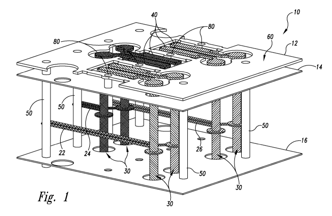
[0012] Figure 1 illustrates a partial isometric view of a multi-layer
printed circuit
board 10 constructed in accordance with an embodiment of the disclosed
technology. The multi-layer circuit board includes an outer top layer 12 and
one or
more inner ground plane layers 14, 16. It will be appreciated by those skilled
in the
art of printed circuit board design that there are generally one or more
additional
layers between layers 14 and 16 such as signal layers, power layers, etc.
-2-
CA 02859778 2014-06-18
WO 2013/103437 PCT/US2012/063044
[0013] In the embodiment of the multi-layer printed circuit board
illustrated,
signals are carried differentially on the board by pairs of traces 22, 24, 26.
In the
embodiment shown, each of these pairs of traces is located on an inner signal
layer
of the multi-layer printed circuit board. Each of the individual signal traces
is
connected to a vertical signal via 30 that extends through the multi-layer
printed
circuit board, so that the signals carried on the traces can change layers in
the
printed circuit board.
[0014] In the embodiment shown, each of the signal vias 30 is electrically
connected to a conductive landing pad 40 that is configured to engage an
electrical
connector (not shown), that is mounted to the multi-layer printed circuit
board. In the
embodiment shown, each landing pad 40 is a rectangular strip of conductive
metal.
The landing pads 40 are aligned in a strip along the top layer of the printed
circuit
board 10. In the embodiment shown, each landing pad is associated with one
signal
of a pair of differentially transmitted signals. The signal vias 30 are
arranged on the
circuit board 10 such that the signal vias 30 that connect to the landing pads
40 are
alternately oriented along the length of the set of the landing pads.
[0015] To reduce cross-talk between signal traces within the printed
circuit
board, the printed circuit board includes a number of grounding vias 50. Each
grounding via 50 is electrically coupled to a ground plane 60 on the outer
layer of the
multi-layer printed circuit board and one or more other ground planes located
on
different inner layers of the multi-layer printed circuit board. The ground
plane 60 on
the outer layer of the multi-layer printed circuit board also extends between
the
landing pads 40 that are associated with different signals. In addition, the
ground
plane 60 surrounds the landing pads 40 and the signal vias 30 in order to
provide
shielding and reduce cross-talk. Cutouts or "anti-pads" in the ground planes
allow
room for the different electrical contacts and the vias on each layer.
[0016] Despite the presence of the grounding vias 50 in the printed circuit
board, many multi-layer printed circuit boards still exhibit some level of
cross-talk
between signals. In accordance with an embodiment of the disclosed technology,
it
has been discovered that one source of the cross-talk occurs between the
adjacent
landing pads 40 that are adapted to engage a connector on the printed circuit
board.
Despite the presence of a ground plane 60 that extends between the landing
pads
associated with different signal traces, cross-talk still occurs.
-3-
CA 02859778 2014-06-18
WO 2013/103437 PCT/US2012/063044
[0017] To further reduce cross-talk occurring between landing pads that are
associated with different signals, a printed circuit board in accordance with
an
embodiment of the disclosed technology includes one or more micro vias 80 that
are
positioned between landing pads 40. Each micro via 80 is electrically coupled
at
one end to the ground plane 60 on an outer layer 12 of the multi-layer printed
circuit
board 10 and at the other end to a ground plane on an inner layer 14 of the
multi-
layer printed circuit board. In the embodiment shown, the inner layer 14 is
adjacent
to the outer layer 12. However, the micro vias 80 may extend further than two
layers
in the multi-layer circuit board if desired.
[0018] In the embodiment shown, the inner layer 14 that connects to an end
of
the micro vias 80 only contains a ground plane and does not contain any signal
traces or other circuit board patterns (power pads, etc.). The ground plane
lies
completely underneath each of the landing pads 40 that engage a connector,
thereby limiting the places where electromagnetic fields can radiate to other
layers of
the printed circuit board. In other embodiments, the inner layer 14 may
include
signal traces or other circuit board patterns if desired.
[0019] Figure 2 illustrates a top view of the multi-layer printed circuit
board 10 in
accordance with an embodiment of the disclosed technology. The printed circuit
board 10 includes landing pads labeled 40a ¨ 40f that are associated with
differential signal traces 22, 24 and 26 respectively. A micro via 80a is
positioned
between landing pads 40b and 40c that are associated with different signals.
Similarly, a micro via 80b is placed between landing pads 40d and 40e that are
associated with different signals. Also shown in Figure 2 are the ground vias
50,
which are positioned outside of the signal vias 30 that connect to the landing
pads
40a-40f.
[0020] In the embodiment shown, the micro vias 80 are symmetrically placed
along the length of the landing pads 40. However the micro vias 80 can also by
asymmetrically placed, (i.e., off center, with respect to the landing pads).
In addition,
there may be more than one micro via 80 positioned between the landing pads
associated with different signals.
[0021] Figure 3 illustrates a cross-section of a multi-layer printed
circuit board
constructed in accordance with an embodiment of the disclosed technology. The
-4-
CA 02859778 2014-06-18
WO 2013/103437 PCT/US2012/063044
cross-section shows the difference in length between the signal vias 30, the
ground
vias 50 and the micro vias 80. In the embodiment shown, the ground vias 50 and
the signal vias 30 extend through the entire thickness of the multi-layer
printed circuit
board 10. However, the micro vias 80 only extend between an outer layer of the
multi-layer printed circuit board and an inner layer of the printed circuit
board. In the
illustrated embodiment, the micro vias 80 extend between an outer layer and a
first
adjacent layer of the multi-layer printed circuit board 10.
[0022] In one embodiment, the micro vias 80 are manufactured by drilling or
laser-etching holes in the multi-layer printed circuit board and filling the
holes with a
conductive material, such as solder. In one embodiment, each micro via 80 has
a
diameter of approximately 0.008 inches. The circuit board is then heated to
form an
electrical connection between the micro vias and the ground planes on the
outer and
inner layers of the circuit board. Although the micro vias are shown as being
round,
other shapes such as; square, rectangular, triangular, hexagonal, etc., could
be
used if desired. With the micro vias 80 placed between the landing pads 40
associated with different signals, computer modeling has shown a reduction of
cross-talk between adjacent signals by an additional -15 dB at 4 GHz, compared
with a printed circuit without the micro vias.
[0023] Although the disclosed embodiment illustrates a circuit board with
landing pads 40 for use with a connector that carries differential signals, it
will be
appreciated that the disclosed technology can also be used to reduce cross-
talk
between landing pads associated with connectors for single-ended signals. In
this
case, one or more micro vias can be placed between each landing pad that is
associated with a different signal.
[0024] In one embodiment, the connector that is coupled to the landing pads
40
on the outer surface of the multi-layer circuit board 10 is a QSH/QTH high-
speed
socket connector produced by Samtec, or the like. However, it will be
appreciated
that other types of connectors associated with other shapes or configurations
of
landing pads could also benefit from the micro vias placed between the landing
pads.
[0025] From the foregoing, it will be appreciated that specific embodiments
of
the invention have been described herein for purposes of illustration, but
that various
-5-
CA 02859778 2014-06-18
WO 2013/103437 PCT/US2012/063044
modifications may be made without deviating from the spirit and scope of the
invention. For example, other configurations of shielding structures such as,
conductive slats, sheets, or the like, can be placed between the landing pads
that
connect to a circuit board connector. Accordingly, the invention is not
limited, except
as by the appended claims.
-6-