Note: Descriptions are shown in the official language in which they were submitted.
CA 2860155 2017-03-10
=
POWERLINE COMMUNICATION RECEIVER
BACKGROUND
Service providers utilize distributed networks to provide services to
customers over
large geographic areas. For example, power companies use power distribution
lines to carry
power from one or more generating stations (power plants) to residential and
commercial
customer sites. The generating stations use alternating current (AC) to
transmit power over
long distances via the power distribution lines. Long-distance transmission
can be
accomplished using a relatively high voltage. Substations located near the
customer sites
provide a step-down from the high voltage to a lower voltage (e.g., using
transformers).
Power distribution lines carry this lower-voltage AC from the substations to
the endpoint
devices customer sites.
Communications providers may utilize a distributed communications network to
provide communications services to customers. Similarly, power companies
utilize a
network of power lines, meters, and other network elements to provide power to
customers
throughout several geographic regions and to receive data from customer
locations
including, but not limited to, data representing metered utility usage.
However, data
communication in a system that contains many thousands of endpoint devices,
each
communicating over the power distribution lines, can be particularly
challenging. The sheer
number of endpoint devices contributes to a host of issues including endpoint
processing
power, memory size, endpoint cost, interference and other concerns. For
instance,
synchronization between an endpoint and a device transmitting downstream to
the endpoint
can be complicated by these and other factors.
SUMMARY
The present disclosure is directed to systems and methods for use with
communications requiring synchronization by a receiver that uses multiple
sampling rates.
These and other aspects of the present disclosure are exemplified in a number
of illustrated
implementations and applications, some of which are shown in the figures.
CA 02860155 2019-06-20
WO 2013/096135 PCT/US2012/069903
2
Certain embodiments of the instant disclosure are directed to decoding of data
communications received at endpoint devices using reduced sampling rates for
portions of
the decoding process. A receiver circuit can be configured and arranged to
decimate an
oversampled version of an input signal. A decimated version of the input
signal can then be
used with various signal processing functions. Consistent with embodiments of
the present
disclosure, the oversampled version can be used to determine synchronization
information
that is used to provide synchronization by adjusting the decimation rate.
Embodiments of the present disclosure are therefore directed toward a circuit-
based
apparatus, and method of using the apparatus. The apparatus is configured with
a
processing circuit and for receiving data communications over power
distribution lines that
carry power using alternating current (AC). The processing circuit can be
configured to
receive an input signal representing the data communications over power
distribution lines.
This input signal can be represented by a modulated carrier wave operating at
the given
frequency. If desired, the input signal can be downconverted to baseband for
signal
processing. If the input signal uses quadrature modulation, then intermediary
signals can be
produced to separate a real portion from an imaginary portion of the input
signal. The
processor can then detect symbol boundaries by processing the intermediary
signals at an
initial (oversampled) sample rate. Decimation is then performed to reduce the
initial sample
rate of the intermediary signals according to a decimation rate. The
intermediary signals,
now sampled at the reduced sample rate, can then be filtered. As discussed
herein, the
decimation can be particularly useful in combination with filters that provide
feedback, as
the feedback may require more memory or processing for higher sampling rates.
The
processing circuit can then determine a timing mismatch between the detected
symbol
boundaries and samples corresponding to the reduced sample rate. The
decimation rate is
then adjusted in response to the determined timing mismatch.
One or more particular embodiments are directed toward a circuit-based
apparatus
for receiving data communications over power distribution lines that carry
power using
alternating current (AC). The apparatus has a processing circuit that is
configured and
arranged to receive an input signal representing the data communications over
power
distribution lines. For a quadrature encoded signal, the input signal is
separated into
intermediary signals representing a real portion and an imaginary portion. The
processing
circuit can then determine timing information from the real portion and the
imaginary
portion. The intermediary signals can then be decimated according to a
variable rate of
CA 2860155 2017-03-10
3
decimation that is responsive to the determined timing information. The
decimated
intermediary signals are also filtered.
Other embodiments are directed toward circuit-based apparatuses, and methods
of
using the apparatuses, for receiving data communications over power
distribution lines that
carry power using altemating current (AC). The apparatus can include one or
more
processing circuits used (or configured and arranged) to receive an input
signal representing
the data communications over power distribution lines. Intermediary signals
are produced
from each of a real portion of an input signal and an imaginary portion of the
input signal.
Symbol boundaries are detected by processing the intermediary signals at an
initial sample
rate. The initial sample rate of the intermediary signals is reduced/decimated
according to a
decimation rate. The intermediary signals are then filtered at the reduced
sample rate. A
timing mismatch is determined between the detected symbol boundaries and
samples
corresponding to the reduced sample rate. The decimation rate is adjusted in
response to the
determined timing mismatch.
Various embodiments of the present disclosure are directed toward a device
having
one or more processing circuits configured and arranged to include or provide
a first
integrator configured to generate a first integration output representing the
integration of a
real portion of a symbol. A second integrator is provided that is configured
to generate a
second integration output representing the integration of an imaginary portion
of the
symbol. Also provided is a signal strength indicator, which is configured to
determine a
signal strength from the first integration output and the second integration
output. A
decimator controller is configured to generate a decimator control signal in
response to the
signal strength. A first decimator is configured to reduce a first sample rate
of the first
integration output to a sample rate that is controlled by the decimator
control signal. A
second decimator is configured to reduce a second sample rate of the second
integration
output to a sample rate that is controlled by the decimator control signal.
Also part of the
device is a first comb filter configured to filter the output of the first
decimator. A second
comb filter is configured to filter the output of the second integrator.
The above summary is not intended to describe each illustrated embodiment or
every implementation of the present disclosure. The figures and detailed
description that
follow, more particularly describe some of these embodiments.
CA 2860155 2017-03-10
=
3a
In one embodiment, the present invention provides a circuit-based apparatus
for
receiving data communications over power distribution lines that carry power
using
alternating current (AC), the apparatus comprising:
a processing circuit configured and arranged to:
receive an input signal representing the data communications over power
distribution lines;
produce intermediary signals from each of a real portion of an input signal
and an imaginary portion of the input signal;
detect symbol boundaries by processing the intermediary signals at an
initial sample rate;
reduce the initial sample rate of the intermediary signals according to a
decimation rate;
filter the intermediary signals at the reduced sample rate;
determine a timing mismatch between the detected symbol boundaries and
samples corresponding to the reduced sample rate; and
adjust the decimation rate in response to the determined timing mismatch.
The processing circuit can be further configured and arranged to detect symbol
boundaries by monitoring the input signal at the initial sample rate and
detecting signal
power peaks occurring between samples corresponding to the reduced sample
rate. The
processing circuit can be further configured and arranged to determine the
timing
mismatch using the number of samples, at the initial sample rate, between a
detected
symbol boundary and a next sample corresponding to the reduced sample rate.
The
processing circuit can be further configured and arranged to use the filtered
intermediary
signals to decode phase-encoded symbols carried by the intermediary signals.
The processing circuit can be further configured and arranged to provide delta
phase discrimination and symbol decoding of the filtered intermediary signals.
The
processing circuit can be further configured and arranged to filter the
intermediary signals
having the reduced sample rate using a comb filter that includes a feedback
component
that is responsive to the decimation rate. The processing circuit can be
further configured
and arranged to determine a timing mismatch for a set of synchronization
symbols by
ignoring timing data for a first two synchronization symbols of the set of
synchronization
symbols.
CA 2860155 2017-03-10
=
3b
In another embodiment, the present invention provides a circuit-based
apparatus
for receiving data communications over power distribution lines that carry
power using
alternating current (AC), the apparatus comprising:
a processing circuit configured and arranged to:
receive an input signal representing the data communications over power
distribution lines;
produce intermediary signals from each of a real portion of an input signal
and an imaginary portion of the input signal;
process the intermediary signals to determine timing information for the
intermediary signals;
decimate the intermediary signals according to a variable rate of
decimation that is responsive to the determined timing information; and
apply a filter to the decimated intermediary signals.
The processing circuit can be further configured and arranged to process the
intermediary signals to determine timing information for the intermediary
signals by
detecting symbol boundaries. The processing circuit can be further configured
and
arranged to demodulate the intermediary signals according to one of quadrature
phase
shift keying (QPSK), differential phase shift keying (DPSK) and frequency
shift keying
(FSK).
In another embodiment, the present invention provides a circuit-based method
for
receiving data communications over power distribution lines that carry power
using
alternating current (AC), the method comprising:
using a processing circuit to:
receive an input signal representing the data communications over power
distribution lines;
produce intermediary signals from each of a real portion of an input signal
and an imaginary portion of the input signal;
detect symbol boundaries by processing the intermediary signals at an
initial sample rate;
reduce the initial sample rate of the intermediary signals according to a
decimation rate;
filter the intermediary signals at the reduced sample rate;
CA 2860155 2017-03-10
3c
determine a timing mismatch between the detected symbol boundaries and
samples corresponding to the reduced sample rate; and
adjust the decimation rate in response to the determined timing mismatch.
The method can further include using the processing circuit to detect symbol
boundaries by monitoring the input signal at the initial sample rate and
detecting signal
power peaks occurring between samples corresponding to the reduced sample
rate. The
method can further include using the processing circuit to determine the
timing mismatch
using the number of samples, at the initial sample rate, between a detected
symbol
boundary and a next sample corresponding to the reduced sample rate. The
method can
further include using the processing circuit to use the filtered intermediary
signals to
decode phase-encoded symbols carried by the intermediary signals.
The method can further include using the processing circuit to provide delta
phase
discrimination and symbol decoding of the filtered intermediary signals. The
method can
further include using the processing circuit to filter the intermediary
signals having the
reduced sample rate using a comb filter that includes a feedback component
that is
responsive to the decimation rate. The method can further include using the
processing
circuit to determine a timing mismatch for a set of synchronization symbols by
ignoring
timing data for a first two synchronization symbols of the set of
synchronization symbols.
The method can further include using the processing circuit to perform the
above
steps for each of multiple channels that have different frequencies. The
method can
further include using the processing circuit to provide bandpass filtering for
the multiple
channels and frequencies.
In another embodiment, the present invention provides a device comprising:
one or more processing circuits configured and arranged to include or provide:
a first integrator configured to generate a first integration output
representing the integration of a real portion of a symbol;
a second integrator configured to generate a second integration output
representing the integration of an imaginary portion of the symbol;
a signal strength indicator configured to determine a signal strength from
the first integration output and the second integration output;
a decimator controller configured to generate a decimator control signal in
response the signal strength;
CA 2860155 2017-03-10
3d
a first decimator configured to reduce a first sample rate of the first
integration output to a sample rate that is controlled by the decimator
control
signal;
a second decimator configured to reduce a second sample rate of the
second integration output to a sample rate that is controlled by the decimator
control signal;
a first comb filter configured to filter the output of the first decimator;
and
a second comb filter configured to filter the output of the second
integrator.
CA 02860155 2019-06-20
WO 2013/096135 PCT/US2012/069903
4
BRIEF DESCRIPTION OF FIGURES
Various example embodiments may be more completely understood in consideration
of the following detailed description in connection with the accompanying
drawings, in
which:
FIG. 1 depicts a block diagram of one or more processing circuits, consistent
with
embodiments of the present disclosure;
FIG. 2 depicts a block diagram for a downstream (endpoint located) receiver,
consistent with embodiments of the present disclosure;
FIG. 3 depicts a block diagram of a complex discrete Fourier transform (CDFT),
consistent with embodiments of the present disclosure;
FIG. 4A is a graph of the frequency response of an experimental (cascaded
integrator comb) CIC filter for M = 1, consistent with embodiments of the
present
disclosure
FIG. 4B is a graph of the frequency response of an experimental CIC filter for
M =
3, consistent with embodiments of the present disclosure;
FIG. 5 depicts a block diagram of an alternative CDFT, consistent with
embodiments of the present disclosure;
FIG. 6 depicts a flow diagram as an example of one way of implementing the
processing and decoding received symbols, consistent with embodiments of the
present
disclosure;
FIG. 7 depicts a flow diagram as an example of one way of implementing a
complex
cascaded integrator comb (CCIC) filter, which is consistent with certain
embodiments of the
present disclosure;
FIG. 8 dcpicts a flow diagram as an example of one way of implementing symbol
synchronization, consistent with embodiments of the present disclosure;
FIG. 9 depicts a flow diagram as an example of one way of determining a
synchronization adjustment amount, consistent with embodiments of the present
disclosure;
FIG. 10A is a graph of an oversampled signal with a synchronization error,
consistent with embodiments of the present disclosure;
FIG. 1 OB is a graph of an oversampled signal with no synchronization error,
consistent with embodiments of the present disclosure; and
CA 02860155 2019-06-20
WO 2013/096135 PCT/US2012/069903
FIG. 11 is a graph of an oversampled signal, consistent with embodiments of
the
present disclosure.
While the disclosure is amenable to various modifications and alternative
forms,
examples thereof have been shown by way of example in the drawings and will be
5 described in detail. It should be understood, however, that the intention
is not to limit the
disclosure to the particular embodiments shown and/or described. On the
contrary, the
intention is to cover all modifications, equivalents, and alternatives falling
within the spirit
and scope of the disclosure.
DETAILED DESCRIPTION
Aspects of the present disclosure are believed to be applicable to a variety
of
different types of devices, systems and arrangements, including those that may
be
implemented for providing synchronization correction. While the present
disclosure is not
necessarily limited to such applications, various aspects of the disclosure
may be
appreciated through a discussion of various examples using this context.
Example embodiments of the instant disclosure are directed to a method,
device,
system or apparatus that is designed to facilitate the decoding of data
communications
received at endpoint devices. For instance, a receiver circuit for an endpoint
can be
configured and arranged to use an oversampled version of a received signal for
a first
processing portion. The oversampled version can then be decimated to a reduced
sample
rate for a second processing portion. The use of a reduced sample rate can be
particularly
useful for reducing processing and/or storage requirements relating to
processing of the
samples. For instance, an accumulator can operate with less operations and a
feedback
component can operate with less memory/storage requirements. Consistent with
embodiments of the present disclosure, the oversampled version can be used to
determine
synchronization information relative to decoding elements that operate on the
reduced
sample rate version of the input signals.
In more particular embodiments of the present disclosure, synchronization can
be
effected by adjusting the rate of decimation. This allows for a fine tuning of
the time at
which the symbol decoding elements receive the samples (where the symbol
decoding
elements operate using the reduced sample rate version of the signals). This
is due to the
decimation rate being linked to the time between selected samples from the
oversampled
version.
Various embodiments of the present disclosure recognize that symbol timing
information can be obtained from the oversampled version without direct
feedback from the
CA 02860155 2019-06-20
WO 2013/096135 PCT/US2012/069903
6
symbol decoding process. Thus, embodiments provide synchronization without a
feedback
loop from symbol decoding logic. More particular embodiments recognize that
this symbol
timing information can be obtained using an algorithm for detecting signal
power from a
mathematical integration of the real and imaginary portions of the oversampled
version of
the signals.
Embodiments of the present disclosure are therefore directed toward a circuit-
based
apparatus, and method of using the apparatus. The apparatus is configured with
a
processing circuit and for receiving data communications over power
distribution lines that
carry power using alternating current (AC). The processing circuit can be
configured to
receive an input signal representing the data communications over power
distribution lines.
This input signal can be represented by a modulated carrier wave operating at
a given
frequency. If desired, the input signal can be downconverted to baseband for
signal
processing. If the input signal uses quadrature modulation, then intermediary
signals can be
produced to separate a real portion from an imaginary portion of the input
signal. The
processor can then detect symbol boundaries by processing the intermediary
signals at an
initial (oversampled) sample rate. Decimation is then performed to reduce the
initial sample
rate of the intermediary signals according to a decimation rate. The
intermediary signals,
now sampled at the reduced sample rate, can then be filtered. As discussed
herein, the
decimation can be particularly useful in combination with filters that provide
feedback, as
the feedback may require more memory or processing for higher sampling rates.
The
processing circuit can then determine a timing mismatch between the detected
symbol
boundaries and samples corresponding to the reduced sample rate. The
decimation rate is
then adjusted in response to the determined timing mismatch.
For particular embodiments of the present disclosure, the filter is a comb
filter that
uses a delay parameter. The delay parameter relates to the time over which
signal
information is stored and used for feedback in the filtering. For a given
delay time, the
amount of stored data is directly related to the sample rate. Thus, if the
sample rate is
reduced, the amount of data stored and/or processed as part of the feedback is
also reduced.
Aspects of the present disclosure recognize that for a given sample rate,
adjustments
to the rate of decimation result in a modification to the time at which
decimated samples are
selected/recorded. Accordingly, the timing of decimated samples, relative to
the input
signal, can be adjusted by changing the decimation rate. The adjustment can be
used to
provide synchronization for subsequent decoding.
CA 2860155 2017-03-10
7
One or more particular embodiments are directed toward a circuit-based
apparatus
for receiving data communications over power distribution lines that carry
power using
alternating current (AC). The apparatus has a processing circuit that is
configured and
arranged to receive an input signal representing the data communications over
power
distribution lines. For a quadrature encoded signal, the input signal is
separated into
intermediary signals representing a real portion and an imaginary portion. The
processing
circuit can then determine timing information from the real portion and the
imaginary
portion. The intermediary signals can then be decimated according to a
variable rate of
decimation that is responsive to the determined timing information. The
decimated
intermediary signals are also filtered.
Consistent with certain embodiments of the present disclosure, the filter
includes a
delay feedback component and the timing information is determined using data
obtained
from integration of the intermediary signals. In some instances, this obtained
data can be
used to determine a received power level for a transmitted symbol.
In certain embodiments, the processing circuits can be configured and arranged
for
use within a communication system that uses power distribution lines to
communicate data
between a command center and endpoint devices using intermediary data-
collecting nodes
(collectors). This type of system can be particularly useful for meter usage
reporting as well
as other functions. For instance, data can be provided from power meters, gas
meters and
water meters, which are respectively installed in gas and water distribution
networks.
Moreover, while the present disclosure generally refers to the endpoints as
providing utility
data (e.g., power) from utility meters, other data can also be communicated.
The interface
to the command center can be implemented using a variety of different
communication
networks including, but not limited to, a wide-area network (WAN) using
Ethernet.
Consistent with embodiments of the present disclosure, each collector can be
configured to be in communication with thousands of endpoints and there can be
thousands
of collectors in connection with a command center. Thus, there can be millions
of total
endpoints and many thousands sharing communications on a common power
distribution
line. Accordingly, embodiments of the present disclosure are directed toward
communicating, coordinating and interpreting data relative to constraints of
the system.
The following discussion provides an overview of various aspects of the system
as relevant
to some of these constraints.
CA 02860155 2019-06-20
WO 2013/096135 PCT/US2012/069903
8
The endpoints can be designed to monitor and report various operating
characteristics of the service network. For example, in a power distribution
network, meters
can monitor characteristics related to power usage in the network. Example
characteristics
related to power usage in the network include average or total power
consumption, power
surges, power drops and load changes, among other characteristics. In gas and
water
distribution networks, meters can measure similar characteristics that are
related to gas and
water usage (e.g., total flow and pressure).
The endpoints report the operating characteristics of the network using
communications channels. In certain embodiments, the communications channels
are
represented by portions of the frequency spectrum. The center frequency and
bandwidth of
each communications channel can depend on the communications system in which
they are
implemented. In some implementations, the communications channels for utility
meters
(e.g., power, gas and/or water meters) can be transmitted using power line
communication
networks that allocate available bandwidth between endpoints according to an
orthogonal
frequency division multiple access (OFDMA) spectrum allocation technique or
another
channel allocation technique.
When the endpoints are implemented as power meters in a power distribution
network, the power meters transmit reporting data that specify updated meter
information.
The updated meter information can include measures of total power consumption,
power
consumption over a specified period of time, peak power consumption,
instantaneous
voltage, peak voltage, minimum voltage and other measures of related to power
consumption and power management (e.g., load information). Each of the power
meters
can also transmit other data, such as status data (e.g., operating in a normal
operating mode,
emergency power mode, or another state such as a recovery state following a
power
outage).
In some implementations, symbols (representing one or more bits representing
reporting and/or the status data) are transmitted on the power distribution
lines over a
specified symbol period. A symbol period is a period of time over which each
symbol is
communicated. A number of symbols are contained within a frame period,
representing the
time over which a complete frame is communicated, wherein each frame provides
synchronization for symbols of the same frame.
According to certain embodiments of the present disclosure, the collectors are
installed in substations and used to control bidirectional communication with
both the
command center (e.g., located at a utility office) and endpoints (e.g.,
located at metering
CA 02860155 2019-06-20
WO 2013/096135 PCT/US2012/069903
9
locations for customer sites). This messaging to the endpoints can be sent to
an individual
endpoint, or broadcast simultaneously to group of endpoints or even sent to
all endpoints
connected to the collectors. Consistent with certain embodiments, the
collectors are built
according to an industrial-grade computer specification in order to withstand
the harsh
environment of a substation.
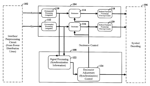
Turning now to the figures, FIG. 1 depicts a block diagram of one or more
processing circuits, consistent with embodiments of the present disclosure.
Consistent with
particular embodiments, the components of FIG. 1 can be located in an endpoint
receiver
that is configured to receive communications carried over power distribution
lines. An
interface circuit 102 can provide isolation from high voltages present on the
power
distribution lines while allowing for the receipt of data transmitted by one
or more
collectors. This can also include filter to remove noise and harmonics
generated by the
power-providing AC present on the power distribution lines. Moreover, for
quadrature
modulation, the interface circuit 102 can separate out the real (Re) and
imaginary portions
(Im) of a received signal. Consistent with certain modulation schemes, these
intermediary
signals can be generated from a downconverted (baseband) version of a received
signal.
Processing circuit(s) 104 and 108 provide functions associated with a high
sampling
rate (oversampled) and a lower/decimated sampling rate. Oversampled processing
functions 110 and 112 can be performed on both the real and imaginary portions
of the
intermediary signals. For instance, the oversampled processing 110 and 112 can
provide an
integrator function based upon thc oversampled rate. This produces an output
signal having
a granularity/accuracy consistent with the oversampled rate.
Decimators 114 and 116 receive the oversampled output of processing functions
110
and 112, respectively. Decimators 114 and 116 then produce an output at a
reduced
sampling rate. The ratio between the input (over)sampling rate and the output
(decimated)
sampling rate represents the decimation rate for decimators 114 and 116. This
decimation
rate can be adjusted as discussed herein.
Decimated sampling functions 118 and 120 can then be undertaken upon the
outputs
of decimators 114 and 116. Aspects of the present disclosure are directed
toward the use of
decimated sampling functions 118 and 120 that have reduced memory and/or
processing
when using lower sampling rates. For instance, the decimated sampling
functions 118 and
120 can include, but are not limited to, a filter that uses a feedback
component that stores
previous samples. In specific embodiments, the filtering represents a comb
filter.
CA 2860155 2017-03-10
=
Symbol decoding 106 can then be performed on the output of the decimated
sampling functions 118 and 120. For instance, the modulation scheme could use
one of
quadrature phase shift keying (QPSK), differential phase shift keying (DPSK)
and
frequency shift keying (FSK). Symbol decoding 106 could be configured to
demodulate
5 accordingly. In a particular instance, symbol decoding 106 can include a
phase delta
discriminator for detecting phase shifts.
Processing circuit(s) 108 can be configured and arranged to generate
synchronization information using signal processing function 122. Signal
processing
function 122 receives oversampled signals from processing functions 110 and
112 and uses
10 this information to generate synchronization information. This
synchronization information
is used to determine a decimator adjustment 124. The decimator adjustment 124
is provided
as a decimator control to change the decimation rate of decimators 1 14 and
116 to provide
synchronization between received signals and processing of the circuits.
In certain embodiments of the present disclosure, signal processing function
122
detects symbol boundaries while decimator adjustment 124 represents an
adjustment made
to align the detected symbol boundaries with the decimated sampling.
FIG. 2 depicts a block diagram for a downstream (endpoint located) receiver,
consistent with embodiments of the present disclosure. The receiver is
configured and
arranged to process communications in multiple different frequency
bands/channels. As
depicted in the figure, a digital input signal is provided to input state 202
from an analog-
to-digital converter (ADC). Input stage 202 can include several band pass
filters (BPFs),
each BPF having a pass frequency corresponding to a respective communication
channel.
Downconverters 204 and 206 can be used to downconvert the filtered signals
according to
an intermediate frequency (F,f). Downconverters 204 and 206 can also be
configured to
separate out real and imaginary portions of the incoming signal by mixing
cosine and sine
signals, respectively.
Consistent with certain embodiments, the sample rate (or sample frequency) of
the
ADC can be a relatively high rate. This can be particularly useful for
bandpass filtering and
downconverting, which can be accomplished with relatively low processing and
memory
requirements for high sample rates. Other functions, however, may become
prohibitively
burdensome at high sample rates. Accordingly, downconverters 204 and 206 can
be
configured to provide decimation to lower the sample rate. The particular
example depicted
in FIG. 2 is a sample rate of 480 Hz, although the receiver and relevant
disclosures are not
limited to this rate.
CA 2860155 2017-03-10
11
According to an embodiment of the present disclosure, harmonic filtering 214
can be
provided to filter out certain frequencies. These filters can be particularly
useful for
filtering harmonics that might be generated by the power-providing AC. This AC
frequency,
and resulting harmonics, can vary around a frequency of about 60 Hz in the
United States
and around 50 Hz in Europe. These standards, however, are relatively arbitrary
and do not
necessarily limit the various embodiments discussed herein.
Processing blocks 208, 210 and 212 receive the outputs of respective harmonic
filters 214. For PSK-encoded symbols, these processing blocks provide delta
phase
discrimination, timing recovery and symbol decoding. More particular functions
include a
complex discrete Fourier transform (CDFT) 216, a power determination 218, a
phase
detector 220, a symbol decoder 222 and a synchronization block 224. CDFT block
216
provides signal processing and filtering useful for decoding symbols. CDFT
block 216 also
provides decimation that reduces the sample rate. The particular example
depicted in FIG.
2 is a reduced sample rate of 10 Hz, although the receiver and relevant
disclosures are not
limited to this rate. Phase detector 220 detects modulations to the phase of
the carrier wave
for the input signal. Symbol decoder 222 decodes the detected phase changes to
generate
corresponding data. Power determination 218 determines the power of the
received signal
as measured by a combination of both the real and imaginary portions of the
signal.
Synchronization block 224 provides a control signal used to change the
decimation
rate of the CDFT block 216. Adjustments to the decimation rate result in a
corresponding
change in thc timing for the selection of the samples. In this manner,
synchronization block
224 can adjust the timing of the components that operate using the reduced
sample rate.
Consistent with certain embodiments of the present disclosure, the
synchronization
block 224 receives input from the CDFT block 216 before decimation to the
reduced sample
rate. In the particular example of FIG. 2, this would correspond to the 480 Hz
sample rate.
Accordingly, the synchronization block 224 can monitor signal parameters using
this higher
sample rate. Synchronization block 224 can use this information to detect
symbol
boundaries. Synchronization block 224 can also receive timing data
corresponding to the
reduced sample rate and determine mismatches between the symbol boundaries and
the
reduced sample rate. For instance, the timing of samples that are taken for
the reduced
sample rate (determined by the decimator) can be synchronized to the phase
detector 220
and/or symbol decoder 222.
In more specific embodiments, the CDFT block 216 can include a filter circuit
with
an integrator function that operates at the higher sample rate. Data from the
integrator can
CA 02860155 2019-06-20
WO 2013/096135 PCT/US2012/069903
12
be provided to the synchronization block 224. Synchronization block 224 uses
this data to
detect symbol boundaries by, for instance, monitoring the signal power.
The various additional diagrams and associated discussion provided hereafter
may
relate to one or more experimental embodiments of the present disclosure.
These
experimental embodiments can be useful in that they provide several reference
points and
illustrative examples. Notwithstanding, the specifics of each experimental
embodiment
may not be required in (or even particularly relevant to) all embodiments of
the present
disclosure.
FIG. 3 depicts a block diagram of a CDFT, consistent with embodiments of the
present disclosure. CDFT block 302 receives the real (Re) and imaginary (Im)
portions of
the data carrying signal. A transformation kernel 304 transforms the real and
imaginary
portions. Kernel 304 operates on the signal sampled at a first (over)sample
rate. The kernel
304 is shown with a particular combination of mixers and combiners; however,
the present
disclosure is not necessarily limited to this specific combination.
The output of kernel 304 is provided to filter block 306. In the particular
embodiment depicted in FIG. 3, filter block 306 operates as a complex cascaded
comb
integrator filter (CCIC). The CCIC filter includes decimators 310. The
decimators 310 are
configured and arranged to provide a variable decimation rate that is
responsive to an
input/control signal or value. The integration function of the CCIC filter is
provided before
the decimators 310 and therefore operates at the higher sample rate. The comb
filter portion
of the CCIC filter is provided after the decimators 310 and therefore operates
at the lower
sample rate. This can be particularly useful for simplifying/reducing the
memory
requirements of the comb filter because the comb filter includes a feedback
component
using previous values(s) as part of the filter.
A signal value from the integrators is provided to the symbol timing and
synchronization block 308. This signal value can be adjusted according to the
feedback
component of the comb filter as shown by the adder symbol. Synchronization
block 308
uses this information to generate a decimator adjustment value. The decimator
adjustment
value is provided to the decimators 310 using input/control signal/value.
In certain embodiments, the decimator adjustment value is calculated as a
function
of a mismatch between the end of a decimation section (defined according to
timings
between decimator samples) and symbol timings (which can be determined by
monitoring
the received power of the data carrying signal).
CA 02860155 2019-06-20
WO 2013/096135 PCT/US2012/069903
13
FIG. 4A is a graph of the frequency response of an experimental CIC filter for
M =
1, consistent with embodiments of the present disclosure. FIG. 4B is a graph
of the
frequency response of an experimental CIC filter for M = 3, consistent with
embodiments of
the present disclosure. For each of FIGs. 4A and 4B, the data represented by
the graph was
generated using a sampling rate: fs = 480 Hz and a decimation rate of 48. The
transfer
function is represented as:
Nr=1
sin("Rf
H(f.) = fs
sin __________________
fs
As shown by the graphs, the experimental data suggest that M = 1 may provide
better filter characteristics, however, the present disclosure is not limited
thereto. For
instance, different input characteristics and operating parameters may suggest
other settings.
FIG. 5 depicts a block diagram of an alternative CDFT, consistent with
embodiments of the present disclosure. Similar to the CDFT of FIG. 3, the CDFT
of FIG. 5
includes a CDFT block 502, a transformation kernel 504, a filter block 506 and
a
synchronization block 508. FIG. 5, however, also includes low pass filter
(LPF) 510 and
512. These LPFs 510 and 512 can be used to filter unwanted interference and
harmonics.
Somewhat unexpectedly, it has been discovered that the LPFs 510 and 512 may
not provide
an appreciable benefit for certain applications. Accordingly, the present
disclosure
contemplates embodiments with and without the LPFs 510 and 512.
FIG. 6 depicts a flow diagram as an example of one way of implementing the
processing and decoding received symbols, consistent with embodiments of the
present
disclosure. The flow diagram can be carried out using one or more processing
circuits,
which can be configured and arranged using, for instance, software-programmed
instructions, hardware circuits and combinations thereof. The processing
circuit(s) begins
processing a particular channel at block 602. In certain embodiments, the
processing circuit
can be configured and arranged to perform this processing on several channels
in parallel.
For instance, an OFDMA protocol can be used and the processing circuit can
monitor
several different frequencies for the OFDMA protocol.
At block 604, the processing circuit is configured and arranged to perform a
complex downconversion of a received signal. A description of a particular
embodiment of
complex downconversion is provided with reference to the kernel of FIGs. 3 and
5.
CA 2860155 2017-03-10
=
14
At block 606, the processing circuit is configured and arranged to perform a
filtering
function. A particular type of filtering is that of a complex cascaded
integrator comb
(CCIC) filter. An embodiment of a processing circuit-implementation of a CCIC
filter is
discussed with reference to FIG. 7.
The processing circuit determines, at block 608, whether or not the end of a
symbol
has been reached. Consistent with embodiments of the present disclosure, the
end of a
symbol is determined based upon the decimator count. If the end of symbol has
been
detected, then the processing circuit can attempt to decode the symbol to
produce
corresponding data bits, as shown by block 610. The processing circuit can
then process
612 the bits accordingly and, if desired, calculate symbol statistics at block
614. The
statistics can include, but are not limited to average symbol power, average
delta phase
error, and maximum delta phase error. If the end of a symbol is not detected,
then further
processing is performed before the symbol is decoded. The process completes at
step 616.
FIG. 7 depicts a flow diagram as an example of one way of implementing a
complex
cascaded integrator comb (CCIC) filter, which is consistent with certain
embodiments of the
present disclosure. The processing circuit begins the filtering process at
block 702 and then
advances to block 704. At block 704 the processing circuit can add the next
sample to an
integrator. The samples at this point have a high (over)sampled rate. The
processing circuit
uses the oversampled (OS) output of the integrator to determine the signal
power (OSPwr)
at block 706. This determined power can be used to calculate the change in
power since the
start of the current symbol. For instance, to determine the symbol power from
both real
(Re0S) and imaginary (ImOS) portions, the processing circuit can use the
formula OSPwr
+ ImOS2.
The processing circuit can then check, at block 708, whether or not the start
of a
symbol period has been reached. In certain embodiments, the symbol period is
assumed to
correspond to the timing of the decimator sampling (absent a timing mismatch).
Decimation can be implemented by taking_every N samples, where N = the
decimation rate
("DecimateBy"). For instance, a decimation count can be incremented for every
received
sample. The received samples are discarded unless the decimation count is
equal to the
decimation rate (or an integer multiple thereof if the count is not reset). A
similar
mechanism is assumed to be used in connection with the flow diagrams; however,
the various
embodiments arc not necessarily limited to such a specific implementation.
Accordingly,
the check 708 can be accomplished by comparing a decimation count to the
decimation rate
(DecimateBy).
CA 2860155 2017-03-10
=
If the start of a symbol is detected by the processing circuit, then the
processing
circuit will initialize storage arrays for each section of the new symbol, per
block 710. And
the array index ("i") can be reset, per block 712. The symbol-based sections
correspond to
different sets of (over)samples within the symbol. For instance, a decimation
rate of 48
5 results in (over)samples 1-48 being included on one symbol period. These
samples can be
broken into four different sections 1-12, 13-24, 25-36 and 37-48. An array
value
(OSPwrMax[i]) can be stored for each section (i).
The processing circuit checks, at block 714, for the end of one of these
sections.
This check can be accomplished, for instance, by comparing the decimation
count against
10 an array value for the current section (OSPwrEnd[i]). If the end of the
current section has
been reached, then the processing circuit prepares for the next session (e.g.,
by incrementing
the section count "I," per block 716).
At block 718, the processing circuit compares the calculated (current) power
(OSPwr) against a stored maximum power for the current section (OSPwerMax[i]).
The
15 current power being above the previous maximum indicates that the power
has increased.
The current power being below the previous maximum indicates that the previous
maximum is a local maximum/peak value (e.g., OSPwrMax[1] of FIG. 10).
When the current power is not above the previous maximum, the processing
circuit
proceeds to block 728. At block 728, the processing circuit checks the current
power
(OSPwr) against a stored minimum power for the current section (OSPwerMin[i]).
The
current power being below the previous minimum indicates that the power has
decreased.
The current power being above the previous minimum indicates that power is
between the
current maximum and minimum powers.
If necessary, the processing circuit updates the minimum power (OSPwerMin[i])
with the current power value (OSPwr) at block 730. The processing circuit also
stores the
decimator count corresponding to new minimum power value. Thereafter, the
processing
circuit proceeds to a synchronization process 726.
When the current power is increasing relative to the previous maximum power,
the
processing circuit proceeds to block 720. At block 720, the processing block
calculates a
threshold value as a function of the current power and a threshold. Consistent
with one
embodiment of the present disclosure, the OSPwrMaxLatchThreshold can set
according to a
predetermined value. For instance, a simulation can be used to model
transmission of test
frames and resulting signals as well as noise and power line harmonics as seen
by the
receiver. The simulation results can then be used to select a value for the
CA 02860155 2019-06-20
WO 2013/096135 PCT/US2012/069903
16
OSPwrMaxLatchThreshold that reduces or minimizes the average delta phase
error. In
other instances, the OSPwrMaxLatchThreshold can be dynamically generated based
upon
actual conditions on the power distribution line. The use of a dynamically
generated
threshold can be particularly useful for adjusting to changes; however, there
can be a
tradeoff in terms of processing resources. When the current power is deemed
sufficient (per
the check of block 722), the processing circuit updates that array values for
the current
section as shown by block 724.
FIG. 8 depicts a flow diagram as an example of one way of implementing symbol
synchronization, consistent with embodiments of the present disclosure. The
synchronization process can be entered once per (over)sample. The processing
circuit
enters the synchronization flow at block 802 and then proceeds to block 804.
At block 804
the decimation count (DeciCount) can be decremented. For instance, the count
can be
initially set to the decimation rate and then decrementcd once per
(over)sample until it
reaches zero, which indicates that a decimated sample should be provided.
Accordingly, the
decimation count reaches zero (determined at block 806), the processing
circuit can assume
that a new symbol period has begun. This particular method of keeping track of
the
decimation count is not meant to be limiting. For instance, there are many
different ways to
track the decimation, including, but not limited to, counting up from zero
and/or detecting
integer multiples of the decimation rate.
If the processor circuit determines that a new symbol period has not been
reached,
then it can exit the synchronization process at block 820. Otherwise, the
processing circuit
can reset the decimation counter to the current decimation rate (DecimateBy),
as shown by
block 808.
For a CIC filter, the processing circuit can also update the comb filter at
step 810.
For instance, the comb filter can use feedback based upon previous values.
These previous
values can be the decimated output of the integrated. Accordingly, the comb
filter can be
updated when a new decimated output is available.
Aspects of the present disclosure are directed toward communication protocols
that
use synchronization symbols that are used by a receiver. The receiver can then
use the
timing from these synchronization symbols to decode subsequent data symbols.
In the
particular communication protocol depicted in FIG. 8, the receiver is
configured to avoid
using the first transmitted synchronization symbol. Thus, the first
synchronization symbol
is effectively skipped because it may be corrupted (e.g., due to internal
adjustment to
receiver clocks). Moreover, the second synchronization symbol is likewise
problematic
CA 02860155 2019-06-20
WO 2013/096135 PCT/US2012/069903
17
because the timing problems of the first synchronization symbol may still be
present during
the next decimation cycle. This skipping of synchronization symbols is
represented by
blocks 812 and 814. In these blocks a synchronization count (DoSynchCount) is
incremented each symbol period and the process exits when the count is less
than 2.
Otherwise, the processing circuit can reset the synchronization count
(DoSynchCount) at block 816. Thereafter, the processing circuit evaluates the
values of the
OSPwr array to calculate a timing adjustment at block 818.
FIG. 9 depicts a flow diagram as an example of one way of determining a
synchronization adjustment amount, consistcnt with embodiments of the present
disclosure.
The processing circuit can enter the process at block 902 in order to
determine an
adjustment amount for the decimator rate, where the adjustment amount is set
to
compensate for a timing mismatch. At block 904, the processing circuit
initializes values
used during the process. One of these values includes the current section
value "i," which is
used to index the array of values previously stored for each section of the
current symbol
period.
At block 906, the processing circuit calculates the difference between the
power
maximum (OSPwrMax) and minimum (OSPwrMin) for the current section. Block 908
represents a check for whether or not this calculated difference exceeds a
threshold value.
If the threshold value is not met, then the processing circuit will advance to
the next section
by incrementing the current section value at block 914. Assuming there are
more sections,
per the check of block 916, the processing circuit will repeat the process for
these section(s).
The failure to meet the threshold will generally indicate that the maximum and
minimum
are identical (or near enough) and therefore there is no synchronization
error.
If the threshold level is exceeded, however, then the processing circuit will
check to
see if the power for the current section exceeds the power from previous
sections, as shown
by block 910. If previous sections have a higher power, then that processing
circuit will
advance to the next section by proceeding to block 914. Otherwise, the
processing circuit
will update the power maximum and synchronization error at block 912. In this
manner, the
processing circuit will use the synchronization error corresponding to the
greatest power.
Once all of the sections have been processed, the processing circuit uses the
stored
synchronization error to determine an adjustment to the decimation rate. For
instance, the
adjustment value can be implemented as an adjustment to the start value for
the decimator
counter. Thus, when the decimator begins counting, it will start at the
decimation rate value
adjusted by the adjustment value. This shifts the time at which the decimator
provides a
CA 2860155 2017-03-10
=
=
18
sample output accordingly. A particular embodiment for a decimator adjustment
is depicted
in table 918. Table 918 includes count adjustments correlated to the
synchronization error
for a base decimation rate of 48. In this instance, the synchronization error
represents the
decimator count value corresponding to the highest OSPwrMax error point
determined
consistent with the process described in FIG. 7. Once the error is determined,
the process
can end per block 920.
FIG. 10 is a graph of an oversampled signal with a synchronization error,
consistent
with embodiments of the present disclosure. The curved line represents the
power value
(e.g., OSPwr = Re0S2 + ImOS2). The entire graph corresponds to one full
decimator cycle.
The power peak, indicated by arrow 1102, represents a likely symbol boundary
point. The
end of the graph, indicated by arrow 1104, represents the desired location of
the symbol
boundary point. The location of arrow 1104 is only 66% of the way to the end
of the graph.
Accordingly, the graph of FIG. 10A represents at 66% error.
FIG. 10B is a graph of an oversampled signal with no synchronization error,
consistent with embodiments of the present disclosure. In FIG. 10B, the end of
the graph
and the peak power coincide as indicated by arrow 1106. This represents
synchronization
or 0% error.
FIG. 11 is a graph of an oversampled signal, consistent with embodiments of
the
present disclosure. The curved line represents the power value (e.g., OSPwr =
Re0S2 +
ImOS2). The dotted vertical lines represent the division point between the
four sections.
According to the various embodiments discussed in the present disclosure, a
maximum
(OSPwrMax[i]) and minimum (OSPwrMin[i] power can be stored for each section
"i." The
decimator count (DeciCount) is also stored for each of the points of maximum
and
minimum power.
Regarding section 0, the maximum and minimum powers are the same value.
Referring back to FIG. 7, the minimum value is set to the maximum value until
and unless
the power begins to decrease after reaching the maximum power. Thus, FIG. 11
shows
maximum and minimum powers being set to the same value, which coincides with
the end
section O. Sections 2 and 3 are similar to section 0 in that the values for
their maximum and
minimum are the same (although the values differ for each section).
Regarding section 1, the maximum and minimum powers are not set to different
values. They would also have different values stored for their respective
decimator counts
(DeciCount[i]).
CA 02860155 2019-06-20
WO 2013/096135 PCT/US2012/069903
19
Referring back to FIG. 9, sections 0, 2 and 3 would not be used to determine
the
synchronization error because the Delta0SPwr would not exceed the threshold
value
(i.e., they would be zero). Section 1, however, has a non-zero value for
Delta0SPwr.
Assuming that this Delta0SPwr value exceeds the threshold value, the maximum
power of
section 1 would determine the synchronization error. In the graph of FIG. 11,
the
DeciCount for this maximum power is 34. The corresponding adjustment value
from table
918 is 9. This adjustment value will then be added to change the decimator
count and
thereby compensate for the error.
The signals and associated logic and functionality described in connection
with the
figures can be implemented in a number of different manners. Unless otherwise
indicated,
various general purpose systems and/or logic circuitry may be used with
programs in
accordance with the teachings herein, or it may prove convenient to construct
a more
specialized apparatus to perform the required method. For example, according
to the
present disclosure, one or more of the methods can be implemented in hard-
wired circuitry
by programming a general-purpose processor, other fully or semi-programmable
logic
circuitry, and/or by a combination of such hardware and a general-purpose
processor
configured with software. In another example, in some context it should be
recognized that
a signal can be represented by one or more digital values shared between
different software
components or modules. Accordingly, the various components and processes shown
in the
figures can be implemented in a variety of circuit-based forms, such as
through the use of
data processing circuit modules.
It is recognized that aspects of the disclosure can be practiced with
computer/processor-based system configurations other than those expressly
described
herein. The required structure for a variety of these systems and circuits
would be apparent
from the intended application and the above description.
The various terms and techniques are used by those knowledgeable in the art to
describe aspects relating to one or more of communications, protocols,
applications,
implementations and mechanisms. One such technique is the description of an
implementation of a technique expressed in terms of an algorithm or
mathematical
expression. While such techniques may be implemented, for example, by
executing code
on a computer, the expression of that technique may be conveyed and
communicated as a
formula, algorithm, or mathematical expression.
CA 02860155 2019-06-20
WO 2013/096135 PCT/US2012/069903
For example, block denoting "C=A+B" as an additive function whose
implementation in hardware and/or software would take two inputs (A and B) and
produce a
summation output (C), such as in combinatorial logic circuitry. Thus, the use
of formula,
algorithm, or mathematical expression as descriptions is to be understood as
having a
5 physical embodiment in at least hardware (such as a processor in which
the techniques of
the present disclosure may be practiced as well as implemented as an
embodiment).
In certain embodiments, machine-executable instructions are stored for
execution in
a manner consistent with one or more of the methods of the present disclosure.
The
instructions can be used to cause a general-purpose or special-purpose
processor that is
10 programmed with the instructions to perform the steps of the methods.
The steps may be
performed by specific hardware components that contain hardwired logic for
performing the
steps, or by any combination of programmed computer components and custom
hardware
components.
In some embodiments, aspects of the present disclosure may be provided as a
15 computer program product, which may include a machine or computer-
readable medium
having stored thereon instructions which may be used to program a computer (or
other
electronic devices) to perform a process according to the present disclosure.
Accordingly,
the computer-readable medium includes any type of media/machine-readable
medium
suitable for storing electronic instructions.
20 The various embodiments described above are provided by way of
illustration and
should not be construed to necessarily limit the disclosure. Based on the
above discussion
and illustrations, those skilled in the art will readily recognize that
various modifications
and changes may be made to the present disclosure without strictly following
the exemplary
embodiments and applications illustrated and described hercin. For instance,
such changes
may include variations on how the decimator count is updated and adjusted.
Such
modifications and changes do not depart from the true spirit and scope of the
present
disclosure, including aspects set forth in the following claims.