Note: Descriptions are shown in the official language in which they were submitted.
CA 02861674 2014-09-02
RUGGEDIZED MULTI-LAYER PRINTED CIRCUIT
BOARD BASED DOWNHOLE ANTENNA
BACKGROUND OF THE INVENTION
Field of the Invention
The preferred embodiments of the present invention are directed generally to
downhole
tools. More particularly, the preferred embodiments are directed to antennas
that allow
azimuthally Sensitive electromagnetic wave resistivity measurements of
formations surrounding
a borehole, and for resistivity-based borehole imaging.
Background of the Invention
Figure 1 exemplifies a related art induction-type logging tool. In particular,
the tool 10
is within a borehole 13, either as a wireline device or as part of a
bottomhole assembly in a
measuring-while-drilling (MWD) process. Induction logging-while-drilling (LWD)
tools of the
related art typically comprise a transmitting antenna loop 12, which comprises
a single loop
extending around the circumference of the tool 10, and two or more receiving
antennas 14A
and 14B. The receiving antennas 14A, B are generally spaced apart from each
other and from
the transmitting antenna 12, and the receiving antennas comprise the same loop
antenna
structure as used for the transmitting antenna 12.
The loop antenna 12, and the receiving loop antennas 14A, B, used in the
related art are
not azimuthally sensitive. In other words, the electromagnetic wave
propagating from the
transmitting antenna 12 propagates in all directions simultaneously. Likewise,
the receiving
antennas 14A, B are not azimuthally sensitive. Thus, tools such as that shown
in Figure 1 are
not suited for taking azimuthally sensitive readings, such as for borehole
imaging. However,
wave propagation tools such as that shown in Figure 1, which operate using
electromagnetic
radiation or electromagnetic wave propagation (an exemplary path of the wave
propagation
shown in dashed lines) are capable of operation in a borehole utilizing oil-
based (non-
conductive) drilling fluid, a feat not achievable by conduction-type tools.
Figure 2 shows a related art conduction-type logging tool. In particular,
Figure 2 shows
a tool 20 disposed within a borehole 22. The tool 20 could be wireline device,
or a part of a
bottomhole assembly of a MWD process. The conduction-type tool 20 of Figure 2
may
comprise a toroidal transmitting or source winding 24, and two secondary
toroidal windings 26
and 28 displaced therefrom. Unlike the induction tool of Figure 1, the related
art conduction
tool exemplified in Figure 2 operates by inducing a current flow into the
fluid within the
borehole 22 and through the surrounding formation 30. Thus, this tool is
operational only in
1
CA 02861674 2014-09-02
environments where the fluid within the borehole 22 is sufficiently
conductive, such as saline
water based drilling fluids. The source 24 and measurement toroids 26 and 28
are used in
combination to determine an amount of current flowing on or off of the tool
20. The source
toroid 24 induces a current flow axially within the tool 20, as indicated by
dashed line 31. A
portion of the axial current flows on (or off) the tool below toroid 28
(exemplified by dashed
line 33), a portion flows on (or off) the tool body between the toroid 26 and
28 (exemplified by
dashed line 35), and further some of the current flows on (or off) the tool at
particular locations,
such as button electrode 32 (exemplified by dashed line 37). Thus, the tool 20
of Figure 2
determines the resistivity of a surrounding formation by calculating an amount
of current flow
induced in the formation as measured by a difference in current flow between
toroid 28 and 26.
As will be appreciated by one of ordinary skill in the art, the current
measurement made by the
toroids 26 and 28 is not azimuthally sensitive; however, for tools that
include a button electrode
32, it is possible to measure current that flows onto or off the button 32,
which is azimuthally
sensitive.
Thus, wave propagation tools such as that shown in Figure 1 may be used in oil-
based
drilling muds, but are not azimuthally sensitive. The conduction tools such as
that shown in
Figure 2 are only operational in conductive environments (it is noted that the
majority of wells
drilled as of the writing of this application use a non-conductive drilling
fluid), but may have
the capability of making azimuthally sensitive resistivity measurements. While
each of the
wave propagation tool of Figure 1 and conduction tool of Figure 2 has its uses
in particular
circumstances, neither device is capable of performing azimuthally sensitive
resistivity
measurements in oil-based drilling fluids.
Thus, what is needed in the art is a system and related method to allow
azimuthally
sensitive measurements for borehole imaging or for formation resistivity
measurements.
BRIEF SUMMARY OF SOME OF THE PREFERRED EMBODIMENTS
The problems noted above are solved in large part by a ruggedized multi-layer
printed
circuit board (PCB) based antenna suitable for downhole use. More
particularly, the
specification discloses an antenna having a ferrite core with windings around
the ferrite core
created by a plurality of conductive traces on the upper and lower circuit
board coupled to each
other through the various PCB layers. The PCB based ferrite core antenna may
be used as
either a source or receiving antenna, and because of its size is capable of
making azimuthally
sensitive readings.
More particularly, the ruggedized PCB based ferrite core antenna may be
utilized on a
downhole tool to make azimuthally sensitive resistivity measurements, and may
also be used to
2
CA 02861674 2014-09-02
make resistivity based borehole wall images. In a first embodiment, a tool
comprises a loop
antenna at a first elevation used as an electromagnetic source. At a spaced
apart location from
the loop antenna a plurality of PCB based ferrite core antennas are coupled to
the tool along its
circumference. The loop antenna generates an electromagnetic signal that is
detected by each
of the plurality of PCB based ferrite core antennas. The electromagnetic
signal received by the
PCB based ferrite core antennas are each in azimuthally sensitive directions,
with directionality
dictated to some extent by physical placement of the antenna on the tool. If
the spacing
between the loop antenna and the plurality of PCB based antennas is relatively
short (on the
order of six inches), then the tool may perform borehole imaging. Using larger
spacing
between the loop antenna and the plurality of PCB based ferrite core antennas,
and a second
plurality of PCB based ferrite core antennas, azinauthally sensitive
electromagnetic wave
resistivity measurements of the surrounding formation are possible.
In a second embodiment, a first plurality of PCB based ferrite core antennas
are spaced
around the circumference of a tool at a first elevation and used as an
electromagnetic source. A
second and third plurality of PCB based ferrite core antennas are spaced about
the
circumference of the tool at a second and third elevation respectively. The
first plurality of
PCB based antennas may be used sequentially, or simultaneously, to generate
electromagnetic
signals propagating to and through the formation. The electromagnetic waves
may be received
by each of the second and third plurality of PCB based antennas, again
allowing azimuthally
sensitive resistivity determinations.
Because the PCB based ferrite core antennas of the preferred embodiment are
capable
of receiving electromagnetic wave propagation in an azimuthally sensitive
manner, and because
these antennas are operational on the philosophy of an induction-type tool, it
is possible to
utilize the antennas to make azimuthally sensitive readings in drilling fluid
environments where
conductive tools are not operable.
The disclosed devices and methods comprise a combination of features and
advantages
which enable it to overcome the deficiencies of the prior art devices. The
various
characteristics described above, as well as other features, will be readily
apparent to those
skilled in the art upon reading the following detailed description, and by
referring to the
accompanying drawings.
BRIEF DESCRIPTION OF THE DRAWINGS
For a detailed description of the preferred embodiments of the invention,
reference will
now be made to the accompanying drawings in which:
Figure 1 shows a related art induction-type tool;
3
CA 02861674 2014-09-02
Figure 2 shows a related art conduction-type tool;
Figure 3 shows a perspective view of a PCB based ferrite core antenna of an
embodiment;
Figure 4 shows yet another view of the PCB based ferrite core antenna;
Figure 5 shows an exploded view of the embodiment of a PCB based ferrite core
antenna shown in Figure 3;
Figure 6 shows an embodiment of use of PCB based ferrite core antennas in a
downhole
tool;
Figure 7 shows a second embodiment of use of PCB based ferrite core antennas
in a
downhole tool;
Figure 8 shows yet another implementation for PCB based ferrite core antennas
in a
downhole tool;
Figure 9 shows placing of the PCB based ferrite core antennas in recesses; and
Figure 10 shows a cap or cover for increasing the directional sensitivity of
PCB based
ferrite core antennas when used as receivers.
NOTATION AND NOMENCLATURE
Certain terms are used throughout the following description and claims to
refer to
particular system components. This document does not intend to distinguish
between
components that differ in name but not function.
In the following discussion and in the claims, the terms "including" and
"comprising"
are used in an open-ended fashion, and thus should be interpreted to mean
"including, but not
limited to.
Also, the term "couple" or "couples" is intended to mean either an indirect
or
direct connection. Thus, if a first device couples to a second device, that
connection may be
through a direct mechanical or electrical (as the context implies) connection,
or through an
indirect mechanical or electrical connection via other devices and
connections.
DETAILED DESCRIPTION OF THE PREFERRED EMBODIMENTS
This specification discloses a ruggedized printed circuit board (PCB) based
ferrite core
antenna for transmitting and receiving electromagnetic waves. The PCB based
antenna
described was developed in the context of downhole logging tools, and more
particularly in the
context of making azimuthally sensitive electromagnetic wave resistivity
readings. While the
construction of the PCB based antenna and its use will be described in the
downhole context,
this should not be read or construed as a limitation as to the applicability
of the PCB based
antenna.
4
CA 02861674 2014-09-02
Figure 3 shows a perspective view of a PCB based ferrite core antenna of the
preferred
embodiments. In particular, the PCB based ferrite core antenna comprises an
upper board 50
and a lower board 52. The upper board 50 comprises a plurality of electrical
traces 54 that span
the board 50 substantially parallel to its width or short dimension. In the
embodiment shown in
Figure 3, ten such traces 54 are shown; however, any number of traces may be
used depending
upon the number of turns required of a specific antenna. At the end of each
trace 54 is a
contact hole, for example holes 56A, B, which extend through the upper board
50. As will be
discussed more thoroughly below, electrical contact between the upper board 50
and the lower
board 52 preferably takes place through the contact holes at the end of the
traces.
Figure 4 shows a perspective view of the antenna of Figure 3 with board 52 in
an upper
orientation. Similar to board 50, board 52 comprises a plurality of traces 58,
with each trace
having at its ends a contact hole, for example holes 60A and B. Unlike board
50, however, the
traces 58 on board 52 are not substantially parallel to the shorter dimensions
of the board, but
instead are at a slight angle. Thus, in this embodiment, the board 52 performs
a cross-over
function such that electrical current traveling in one of the traces 54 on
board 50 crosses over
on the electrical trace 58 of board 52, thus forcing the current to flow in
the next loop of the
overall circuit.
Referring somewhat simultaneously to Figure 3 and 4, between the board 50 and
board 52 reside a plurality of intermediate boards 62. The primary function of
an intermediate
board 62 is to contain the ferrite material between board 50 and board 52, as
well as to provide
conduction paths for the various turns of electrical traces around the ferrite
mat&cial. In the
perspective views of Figures 3 and 4, the board 52 is elongated with respect
to board 50, and
thus has an elongated section 64 (Figure 3). In this embodiment, the elongated
section 64 of
board 52 has a plurality of electrical contacts, namely contact points 66 and
68. In this
embodiment, the contact points 66 and 68 are the location where electrical
contact is made to
the PCB based ferrite core antenna. Thus, these are the locations where
transmilt circuitry is
coupled to the antenna for the purpose of generating electromagnetic waves
within the
borehole. Likewise, since the PCB based ferrite core antennas may be also used
as receiving
antennas, the electrical contact points 66 and 68 are the location where
receive circuitry is
coupled to the antenna.
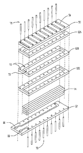
Figure 5 shows an exploded perspective view of the PCB based ferrite core
antenna
Figures 3 and 4. In particular, Figure 5 shows board 50 and board 52, with =
the various
components normally coupled between the two boards in exploded view. Figure 5
shows three
intermediate boards 62A, B and C, although any number may be used based on the
thickness of
the boards, and the amount of ferrite material to be contained therein, and
whether
5
CA 02861674 2014-09-02
it is desirable to completely seal the ferrite within the boards. Each of the
intermediate boards
62 comprises a central hole 70, and a plurality of interconnect holes 72
extending along the
long dimension. As the intermediate boards 62 are stacked, their central holes
form an inner
cavity where a plurality of ferrite elements 74 are placed. The intermediate
boards 62, along
with the ferrite material 74, are sandwiched between the board 50 and the
board 52. In one
embodiment, electrical contact between the traces 54 of board 50 and the
traces 58 of board 52
(not shown in Figure 5) is made by a plurality of contact wires or pins 76.
The contact pins 76
extend through the contact holes 56 in the upper board, the holes 72 in the
intermediate boards,
and the holes 60 in board 52. The length of the contact pins is dictated by
the overall thickness
Further, Figure 5 shows how the contacts 66 and 68 electrically couple to the
traces 54
and 58. In particular, in the embodiment shown in Figure 5, the electrical
contact 66 extends
along the long dimension of board 52, and surrounds a contact hole at the far
end. Whether the
6
CA 02861674 2014-09-02
connection pins 76, 78 are used, or whether other techniques for connecting
traces on multiple
levels of circuit board are used, preferably the trace 66 electrically couples
to the winding
created by the traces 54, traces 58 and interconnections between the traces.
Likewise, the
connection pad 68 electrically couples to a trace that surrounds a closest
contact hole on the
opposite side of the connection made for pad 66. Through techniques already
discussed, the
contact point 68 is electrically coupled to the windings of the antenna.
Although not
specifically shown in Figure 5, the ferrite core 74 is electrically isolated
from the traces. This
isolation may take the form of an insulating sheet, or alternatively the
traces could be within the
non-conductive board 52 itself.
Before proceeding, it must be understood that the embodiment shown in Figures
3, 4
and 5 is merely exemplary of the idea of using traces on a printed circuit
board, as well as
electrical connections between various layers of board, to form the windings
or turns of
electrical conduction path around a ferrite core held in place by the PCBs. In
one embodiment,
the ferrite core is sealed within the inner cavity created by the intermediate
boards by having
those intermediate boards seal to each other. However, depending on the type
of ferrite
material used, or the proposed use of the antenna (or both), it would not be
necessary that the
intermediate boards seal to one another. Instead, the connecting pins 76 and
78 could suspend
one or more intermediate boards between the boards 50, 52 having the
electrical traces, thus
keeping the ferrite material within the cavity defined by the intermediate
boards, and also
keeping the ferrite material from coming into electrical contact with the
connecting pins.
Further, the embodiment of Figures 3, 4 and 5 has extended portions 64 of
board 52 to provide
a location for the electrical coupling of signal wires. However, this extended
portion 64 need
not be present, and instead the wires for electrically coupling the PCB based
ferrite core
antenna could solder directly to appropriate locations on the antenna. Further
still, depending
upon the particular application, the PCB based ferrite core antenna may also
itself be
encapsulated in a protective material, such as epoxy, in order that the board
material not be
exposed to the environment of operation. Further still, techniques exist as of
the writing of this
specification for embedding electrical traces within a printed circuit board
such that they are not
exposed, other than their electrical contacts, on the surfaces of the printed
circuit board, and this
technology too could be utilized in creating the board 50 and board 52.
Moreover, an
embodiment of the PCB based ferrite core antenna such as that shown in Figures
3, 4 and 5
may have a long dimension of approximately 8 centimeters, a width
approximately 1.5
centimeters and a height of approximately 1.5 centimeters. A PCB based ferrite
core antenna
such as that shown in Figures 3, 4 and 5 with these dimensions may be suitable
for azimuthally
7
CA 02861674 2014-09-02
sensitive formation resistivity measurements. In situations where borehole
imaging is
desired, the overall size may become smaller, but such a construction does not
depart from
the scope of this invention.
Figure 6 shows an embodiment utilizing the PCB based ferrite core antennas. In
particular, Figure 6 shows a tool 80 disposed within a borehole 82. The tool
80 could be a
wireline device, or the tool 80 could be part of a bottomhole assembly of a
measuring-
while-drilling (MWD) system. In this embodiment, the source is a loop antenna
84. As is
known in the art, a loop antenna 84 generates omni-directional electromagnetic
radiation.
The tool 80 of the embodiment shown in Figure 6 also comprises a first
plurality of PCB
based ferrite core antennas 86 coupled at a location on the tool 80 having a
spacing S from
the loop antenna 84, and a second plurality of PCB based ferrite core antennas
87 coupled
to the tool below the first plurality. Figure 6 shows only three such PCB
based ferrite core
antennas in the first and second plurality (labeled 86A, B, C and 87A, B, C);
however, any
number of PCB based ferrite core antennas may be spaced along the
circumference of the
tool 80 at these locations. Preferably, however, eight PCB based ferrite core
antennas 86 are
evenly spaced around the circumference of the tool 80 at each of the first and
second
pluralities. Operable embodiments may have as few as four antennas, and high
resolution
tools may comprises sixteen, thirty-two or more. The source antenna 84 creates
electromagnetic wave, and each of the PCB based ferrite core antennas 86, 87
receives a
portion of that propagating electromagnetic wave. Because the PCB based
ferrite core
antennas are each disposed at a particular circumferential location, and
because the
antennas are mounted proximate to the metal surface of the tool 80, the
electromagnetic
wave received is localized to the portion of the borehole wall or formation
through which
that wave propagated. Thus, having a plurality of PCB based ferrite core
antennas allows, in
this embodiment, taking of azimuthally sensitive readings. The type of
readings are
dependent, to some extent, on the spacing S between the plurality of antennas
86 and the
loop antenna 84. For spacings between the source and the first plurality 86 on
the order of
six inches, a tool such as that shown in Figure 6 may be particularly suited
for performing
electromagnetic resistivity borehole wall imaging. In this arrangement, the
second plurality
87, if used, may be spaced approximately an inch from receivers 86. For
greater spacings,
on the order of eight inches or more to the first plurality 86 and fourteen to
eighteen inches
to the second plurality, the tool may be particularly suited for making
azimuthally sensitive
formation resistivity measurements.
Referring now to Figure 7, there is shown an alternative embodiment where,
rather
than using a loop antenna as the source, a plurality of PCB based ferrite core
antennas are
8
=
CA 02861674 2014-09-02
themselves used to generate the electromagnetic waves source. In particular,
Figure 7 shows a
tool 90 disposed within a borehole 92. The tool 90 could be a wireline device,
or also could be
a tool within a bottomhole assembly of an MWD process. In this embodiment,
electromagnetic
waves source are generated by a plurality of PCB based ferrite core antennas
94, whose
construction was discussed above. Although the exemplary drawing of Figure 7
shows only
three such antennas 94A, B and C, any number of antennas may be spaced around
the
circumference of the tool, and it is preferred that eight such antennas are
used. Similar to the
embodiment shown in Figure 6, the embodiment of Figure 7 comprises a first and
second
plurality of PCB based ferrite core antennas 96, 97, used as receivers, spaced
along the
circumference of the tool 90 at a spaced apart location from the plurality of
transmitting
antennas 94. In the perspective view of Figure 7, only three such receiving
antennas 96A, B
and C are visible for the first plurality, and only three receiving antennas
97A, B and C are
visible for the second plurality; however, any number of antennas may be used,
and preferably
eight such antennas are utilized at each of the first and second plurality.
Operation of the
tool 90 of Figure 7 may alternatively comprise transmitting electromagnetic
wave with all of
the transmitting antennas 94 simultaneously, or may alternatively comprise
firing each of the
transmitting antennas 96 sequentially. In a fashion similar to that described
with respect to
Figure 6, receiving the electromagnetic wave generated by the source antennas
94 is
accomplished with each individual receiving antenna 96, 97. By virtue of
circumferential
spacing about the tool 90, the electromagnetic wave propagation received is
azimuthally
sensitive. A tool such as that shown in Figure 7 may be utilized for borehole
imaging as
previously discussed, or may likewise be utilized for azimuthally sensitive
formation resistivity
measurements.
Figure 8 shows yet another embodiment of an electromagnetic wave resistivity
device
using the PCB based ferrite core antennas as described above. In particular,
Figure 8 shows a
tool 100 disposed within a borehole 102. The tool 100 may be a wireline
device, or the tool
may be part of a bottomhole assembly of a MWD operation. In the embodiment
shown in
Figure 8, the tool 100 comprises one or more stabilizing fins 104A, B. In this
embodiment, the
PCB based ferrite core antennas are preferably placed within the stabilizing
fin 104 near its
outer surface. In particular, the tool may comprise a source antenna 106 and a
receiving
antenna 108 disposed within the stabilizer fin 104A. It is noted in this
particular embodiment
that the tool 100 may serve a dual purpose. In particular, the tool 100 may be
utilized for other
functions, such as neutron porosity, with the neutron sources and sensors
disposed at other
locations in the tool, such as within the stabilizing fin 104B. Operation of a
tool such as tool
9
CA 02861674 2014-09-02
100 is similar to the previous embodiments in that the source antenna 106
generates
electromagnetic wave, which is received by the receiving antenna 108. By
virtue of the
receiving antenna's location on a particular side of a tool 100, the
electromagnetic wave
radiation received is azimuthally sensitive. If the tool 100 rotates, borehole
imaging is possible.
An additional receiver antenna could be placed within the stabilizing fin 104A
which allows
azimuthally sensitive resistivity measurements.
Although it has not been previously discussed, Figure 9 indicates that the
source
antenna 106 and the receiving antenna 108 are mounted within recesses. In
fact, in each of the
embodiments of Figures 6, 7 and 8, the preferred implementation is mounting of
the PCB base
ferrite core antennas is in recesses on the tool. With respect to Figures 6
and 7, the recesses are
within the tool body itself. With respect to Figure 8, the recesses are on the
stabilizing fin
104A. Although the printed circuit board based ferrite core antennas, if
operated in free space,
would be omni-directional, because of their small size relative to the tool
body, and the fact
they are preferably mounted within recess, they become directionally
sensitive. Additional
directional sensitivity is accomplished by way of a cap arrangement.
Figure 10 shows an exemplary cap arrangement for covering the PCB based
ferrite core
antennas to achieve greater directionality. In particular, cap 110 comprises a
hollowed out
inner surface 114, having sufficient volume to cover a PCB based ferrite core
antenna. In a
front surface of the cap 100, there is a slot 112. Operation of the cap 110 in
any of the
embodiments involves placing the cap 110 over the receiving antenna (86, 96 or
108) with the
cavity 112 covering the PCB based ferrite core antenna, and the slot 112
exposed to an outer
surface of the tool (80, 90 or 100). Electromagnetic wave radiation,
specifically the magnetic
field components, created by a source (whether a loop or other PCB based
ferrite core antenna)
could access, and therefore induce a current flow in, the P03 based ferrite
core antenna within
the cap through the slot 112. The smaller the slot along its short distance,
the greater the
directional sensitivity becomes; however, sufficient slot is required such
that the
electromagnetic wave radiation may induce sufficient current for detection.
Although not specifically shown in the drawings, each of the source antennas
and
receiving antennas is coupled to an electrical circuit for broadcasting and
detecting
electromagnetic signals respectively. One of ordinary skill in the art, now
understanding the
construction and use of the PCB based ferrite core antennas will realize that
existing electronics
used in induction-type logging tools may be coupled to the PCB based ferrite
core antennas for
operational purposes. Thus, no further description of the specific electronics
is required to
CA 02861674 2014-09-02
apprise one of ordinary skill in the art how to use the PCB based ferrite core
antennas of the
various described embodiments with respect to necessary electronics.
The above discussion is meant to be illustrative of the principles and various
embodiments of the present invention. Numerous variations and modifications
will become
apparent to those skilled in the art once the above disclosure is fully
appreciated. For example,
in the embodiments shown in Figures 6 and 7, there are two levels of receiving
antennas. For
formation resistivity measurements, having two levels of receiving antennas
may be required,
such that a difference in received amplitude and difference in received phase
may be
determined. For use of the PCB based ferrite core antennas in borehole imaging
tools, the
second level of receiving antennas is optional. Correspondingly, the
embodiment shown in
Figure 8 having only one transmitting antenna and one receiving antenna, thus
particularly
suited for borehole wall imaging, may likewise include an additional receiving
antenna and,
with proper spacing, may also be used as a formation resistivity testing
device. It is intended
that the following claims be interpreted to embrace all such variations and
modifications.
11