Note: Descriptions are shown in the official language in which they were submitted.
CA 02861779 2014-08-28
270922
METHOD FOR OPERATING AN ELECTRICAL CIRCUIT AND
ELECTRICAL CIRCUIT
[0001] The invention relates to a method for operating an
electrical circuit and a corresponding electrical circuit.
[0002] From publication DE 10 2010 046 142 Al an electrical
circuit has been known, said circuit being composed of a
plurality of modular switches. As a result of an appropriate
arrangement and activation of the power semiconductor components
of the modular switches it is possible, in doing so, to embody
the electrical circuit as a converter, i.e., for the conversion
of a direct voltage into an alternating voltage, or vice versa.
Consequently, the electrical circuit can be used, in particular,
for the transmission of energy with high direct voltages.
[0003] Referring to DE 10 2010 046 142 Al, the current can flow
across the modular switches in only one direction. Therefore, if
the known electrical circuit is used, for example in high-voltage
direct current (HVDC) transmission, this has the result that a
reversal of the direction of energy transmission can be achieved
only in that the direct voltage is reversed. However, in the case
of a unipolar undersea cable this is possible only within
considerable constraints.
[0004] It is the object of the present invention to improve the
known electrical circuit.
[0005] The invention achieves this object with a method as in
Claim 1 and Claim 4, as well as well as with an electrical
circuit as in Claim 2.
[0006] The electrical circuit in accordance with the invention
comprises at least one modular switch, wherein the modular switch
is provided with a first series circuit comprising a first
controllable power semiconductor component and a first diode, and
with a second series circuit comprising a second diode and a
1
CA 02861779 2014-08-28
270922
second controllable semiconductor component; wherein the
connecting point of the first power semiconductor component and
the first diode form a first connection, and the connecting point
of the second diode and the second power semiconductor component
form a second connection of the modular switch; wherein, in the
first series circuit, the first power semiconductor component is
connected in parallel to a third diode, and the first diode is
connected in parallel to a third controllable power semiconductor
element; wherein, in the second series circuit, the second power
semiconductor component is connected in parallel to a fourth
diode, and the second diode is connected in parallel to a fourth
controllable power semiconductor component; wherein the
conducting directions of the third diode and the third power
semiconductor component correspond to the conducting directions
of the first diode and the first power semiconductor component,
and the conducting directions of the fourth diode and the fourth
power semiconductor component correspond to the conducting
directions of the second diode and the second power
semiconductor; wherein the modular switch is provided with a
capacitor; and wherein the first series circuit and the second
series circuit and the capacitor of the modular switch are
connected in parallel relative to each other.
[0007] Referring to the method in accordance with the invention,
either both the first and second power semiconductor components
are connected so as to be conducting, and both the third and
fourth power semiconductor components are controlled so as to be
blocking, so that a current from the first connection flows
across the first power semiconductor component, across the
capacitor and across the second power semiconductor component to
the second connection, or both the third and fourth power
semiconductor components are connected so as to be conducting,
and both the first and second power semiconductor components are
controlled so as to be blocking, so that the current flows in
reverse direction from the second connection across the fourth
power semiconductor component, across the capacitor and across
the third power semiconductor component to the first connection.
2
CA 02861779 2014-08-28
270922
[0008] The invention features the advantage that the current can
flow through the modular switches in both directions. This may be
achieved with an appropriate activation of the modular switches.
In doing so, it is possible for electrical energy in the form of
a direct current to be carried in both directions across power
converters that comprise the modular switches.
[0009] Referring to the electrical circuit in accordance with
the invention, a voltage reversal of the direct voltage is not
necessary. Among other things, this brings about the advantage
that unipolar cables can be used in direct-voltage transmission.
[0010] If the invention is applied, for example, in the energy
transmission of high direct voltages within a meshed direct-
voltage network, it is possible to freely adjust the direct
voltages that are used for energy transmission. In this manner,
it is possible - even in the case of an error situation - to
limit the direct voltage to one transmission section and to thus
be able to respond to the error situation.
[0011] Furthermore, the invention features substantial
advantages in error and short circuit situations. Therefore, if,
in a meshed direct voltage network, as many as possible or all
current converters are capable of changing the direct voltage and
thus limit the direct current, it is possible - after an error or
a short circuit has been detected - to first limit the error or
short circuit current at the error or short circuit location with
the use of the invention in order to subsequently, for example,
completely break and galvanically separate the error current or
short circuit current, for example with the help of common,
already commercially available, circuit breakers.
[0012] Additional features, possibilities of use and advantages
of the invention can be inferred from the description of the
exemplary embodiments of the invention hereinafter, said
exemplary embodiments being illustrated in the related figures.
In doing so, the object of the invention is represented by each
of the described or illustrated examples, individually or in any
3
CA 02861779 2014-08-28
270922
combination, and independently of their summarization or their
citation or illustration in the description, or in the figures.
They show in:
[0013] Figure 1 a schematic block circuit diagram of an
exemplary embodiment of an electrical circuit;
[0014] Figures 2 and 3 sections of the electrical circuit of
Figure 1;
[0015] Figure 4a a schematic block circuit diagram of an
application of the electrical circuit of Figure 1; and
[0016] Figure 4b a schematic time-dependency diagram of current
and voltage characteristics as in Figure 4a.
[0017] Figure 1 shows an electrical circuit 10 that can
preferably be used within the framework of a so-called high-
voltage direct current (HVDC) transmission. In particular, the
circuit 10 may be used for connecting two existing electrical
power supply networks in order to transmit electrical energy
between the power supply networks in both directions. Hereinafter
follows a description of the direction of the current flow during
normal operation, i.e., for the operation in which the current
flows through clocked power semiconductor components and not in
their anti-parallel diodes. Other current flows in opposite
directions are possible, however, they will not be specifically
described here.
[0018] The circuit 10 comprises a first converter 11 and a
second converter 12. The first converter 11 is connected to a
first transformer 13 on its alternating-voltage side, and the
second converter 12 is connected to a second transformer 14 on
its alternating voltage side. Each of the converters 11, 12, the
transformers 13, 14 and their electrical connections are three-
phased in the present exemplary embodiment.
[0019] On their direct-voltage side, the two converters 11, 12
are connected to each other by way of two electrical lines 15,
4
CA 02861779 2014-08-28
270922
16. Inductances 17, 18 may exist between the converters 11, 12
and the lines 15, 16.
[0020] Each of the two converters 11, 12 is disposed to convert
a direct voltage into an alternating voltage, or vice versa. The
two transformers 13, 14 are disposed to adapt the voltage on the
alternating-voltage side of the respectively associate converter
11, 12 to the existing boundary conditions.
[0021] A direct voltage is applied between the two electrical
lines 15, 16. Specifically, this is a high voltage, for example
320 kV. The length of the two lines 15, 16 may be several
kilometers, for example 100 km. One of the two lines 15, 16, for
example line 16, may be grounded. Preferably, a high-voltage
direct current (HVDC) transmission can be implemented by way of
the two lines 15, 16.
[0022] Each of the converters 11, 12 is composed of a plurality
of modular switches 21, 22. Due to the exemplary three-phase
embodiment, the modular switches 21, 22 in each of the two
converters 11, 12 are arranged in three groups. Each of the
groups of each converter 11, 12 includes the same number of
modular switches 21, 22. As will still be explained hereinafter,
a three-step embodiment of the respective converter requires,
respectively, two modular switches 21, 22 per group, a five-step
embodiment requires respectively four modular switches 21, 22,
and so on.
[0023] It is understood that the number of phases of the circuit
may also be greater or smaller than three. Likewise, the
number of phases of the two converters 11, 12 or the associate
transformers 13, 14 may also be different. Likewise, the number
of modular switches 21, 22 per group in the two converters 11, 12
may also be different. Instead of a transformer, it is also
possible to use a throttle for a solution not using a
transformer.
5
CA 02861779 2014-08-28
270922
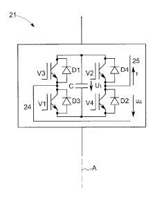
[0024] Figure 2a shows the modular switch 21 that is provided in
the converter 11.
[0025] The modular switch 21 has a first series circuit
comprising a first controllable power semiconductor component V1
and a first diode D1, as well as a second series circuit
comprising a second diode D2 and a second controllable power
semiconductor component V2.
[0026] In a first series circuit, the collector of the first
power semiconductor component V1 and the anode of the first diode
D1 are connected to each other. This connecting point is referred
to as the first connection 24. In the second series circuit, the
emitter of the second power semiconductor component V2 and the
cathode of the second diode D2 are connected to each other. This
connecting point is referred to as the second connection 25.
[0027] The two series circuits are connected in parallel
relative to each other. Consequently, the cathode of the first
diode D1 is connected to the collector of the second power
semiconductor component V2, and the emitter of the first power
semiconductor component V1 is connected to the anode of the
second diode D2.
[0028] In the first series circuit, a third diode D3 is
connected in parallel to the first power semiconductor component
V1, and the first diode D1 is connected in parallel to a third
power semiconductor component V3. The conducting directions of
the third diode D3 and of the third power semiconductor component
V3 correspond to the conducting directions of the first diode D1
and the first power semiconductor components Vi. Correspondingly,
the second power semiconductor component V2 is connected in
parallel to a fourth diode D4, and the second diode D2 is
connected in parallel to a fourth power semiconductor component
V4.
[0029] A capacitor C is connected in parallel to the two series
circuits that are connected in parallel.
6
CA 02861779 2014-08-28
270922
[0030] A direct voltage ucic is applied to the capacitor C, and a
connecting voltage ua exists between the two connections 24, 25.
The direction of the aforementioned voltages is indicated in
Figure 2a. Furthermore, a current i flows from the first
connection 24 in the direction to the second connection 25.
[0031] Referring to the power semiconductor components V1, V2,
V3, V4, these are controllable switches, for example,
transistors, in particular field effect transistors, or
thyristors with an optionally required auxiliary protective
element, in particular gate turn-off (GTO) thyristors or
insulated gate bipolar transistors (IGBTs), or comparable
electronic components. Depending on the embodiment of the power
semiconductor components V1, V2, V3, V4, their connections may be
identified in different ways. The aforementioned terms collector
and emitter relate to the exemplary use of IGBTs. The capacitor C
may be configured so as to be unipolar.
[0032] The modular switch 21 is able to assume the following
states:
- If the power semiconductor components V1, V2, V3, V4 are
switched off (blocking), the current i can flow either from the
first connection 24 across the diode D1, across the capacitor C
and across the diode D2 to the second connection 25 or, in
reverse direction, from the second connection 25 across the diode
D4, across the capacitor C and across the diode D3, to the first
connection 24. In both cases, the capacitor C is charged by the
flowing current i or by the reversely flowing current i so that
the direct voltage udc becomes higher. Apart from the voltage
drops on the diodes D1, D2 and D3, D4, respectively, the
connecting voltage ua is equal to the negative direct voltage -
udc, therefore ua = -udc, or equal to the positive direct voltage
*lc; therefore ua =
- If both the power semiconductor components V1, V2 are switched
on (conducting) and both the power semiconductor components V3,
V4 are switched off (blocking), the current i - normal mode -
7
CA 02861779 2014-08-28
270922
flows from the first connection 24 across the first power
semiconductor component V1, across the capacitor C and across the
second power semiconductor component V2 to the second connection
25. The capacitor C is discharged by this current i so that the
direct voltage udc decreases. Apart from the voltage drops on the
power semiconductor components V1, V2, the connecting voltage ua
is equal to the positive direct voltage udc; therefore ua = udc.
= - If both the power semiconductor components V3, V4 are switched
on (conducting) and both the power semiconductor components V1,
V2 are switched off (blocking), the current i flows in reverse
direction from the second connection 25 across the fourth power
semiconductor component V4, across the capacitor C and across the
third power semiconductor component V3 to the first connection
24. The capacitor C is discharged by this current 1, so that the
direct voltage ud, becomes lower. Apart from the voltage drops on
the power semiconductor components V3, V4, the connecting voltage
ua is equal to the negative direct voltage -ud,.; therefore ua = -
Udc =
- If the first power semiconductor component V1 is switched on
(conducting) and the power semiconductor components V2, V3, V4
are switched off (blocking), the current 1 flows from the first
connection 24 across the first power semiconductor component V1
and across the second diode D2 to the second connection 25. The
direct voltage ud, on the capacitor C remains constant. Apart from
the voltage drops on the first power semiconductor component V1
and the second diode 2, the connecting voltage ua is equal to
zero; therefore ua = 0.
- If the power semiconductor components V1, V3, V4 are switched
off (blocking) and the second power semiconductor component V2 is
switched on (conducting), the current i flows from the first
connection 24 across the first diode D1 and the second power
semiconductor component V2 to the second connection 25. The
direct voltage udc on the capacitor C remains constant. Apart from
the voltage drops on the first diode D1 and the second power
8
CA 02861779 2014-08-28
270922
semiconductor component V2, the connecting voltage ua is equal to
zero; therefore ua = 0.
- If the third power semiconductor component V3 is switched on
(conducting) and the power superconductor components V1, V2, V4
are switched off (blocking), the current i flows in reverse
direction from the second connection 25 across the fourth diode
D4 and across the third power semiconductor component V3 to the
first connection 24. The direct voltage udc on the capacitor C
remains constant. Apart from the voltage drops on the third power
semiconductor component V3 and the fourth diode D4, the
connecting voltage ua is equal to zero; therefore ua = 0.
- If the power semiconductor components V1, V2, V3 are switched
off (blocking) and the fourth power semiconductor component V4 is
switched on (conducting), the current i flows in reverse
direction from the second connection 25 across the fourth power
semiconductor component V4 and the third diode D3 to the first
connection 24. The direct voltage uac on the capacitor C remains
constant. Apart from the voltage drops on the third diode D3 and
the fourth power semiconductor component V4, the connecting
voltage ua is equal to zero; therefore ua = 0.
[0033] Consequently, the current through the modular switch 21
is able to flow in both directions.
[0034] In both cases, i.e., independent of the direction in
which the current flows through the modular switch 21, the
connecting voltage ua can essentially assume three values, i.e.,
ua = Udc or ua = Udc or ua = 0. In doing so, the direct voltage ucic
on the capacitor C may increase or decrease.
[0035] Figure 2b shows how the modular switch 21 of Figure 2a is
switched within one of the groups of the converter 11. In doing
so, the right group of the converter 11 of Figure 1 is shown as
an example. The other groups of the converter 11 are configured
accordingly.
9
CA 02861779 2014-08-28
270922
[0036] Figure 2b shows two modular switches 21 per group as an
example. In accordance with Figure 2b, the two modular switches
21 are connected in series. The connection 25 of the upper
modular switch 21 is connected to a positive pole of the
converter 11 on the direct-voltage side and thus connected to the
line 15. The connection 24 of the lower modular switch is
connected to a negative pole of the converter 11 on the direct-
voltage side and thus connected to line 16. The connecting point
of the two modular switches 21 represents the associate phase of
the converter 11 on the alternating-voltage side and is connected
to the transformer 13.
[0037] The explained embodiment of the converter 11 means that
the converter 11 is a three-phase converter. The voltage of the
associate alternating-voltage side phase of the converter 11 can
thus essentially assume a positive state or a negative state, or
a zero state.
[0038] Referring to Figure 3a, the modular switch 22 is shown
comprising the converter 12.
[0039] Considering its design, the modular switch 22 of Figure
3a essentially corresponds to the modular switch 21 of Figure 2a.
When visualized, the modular switch 22 of Figure 3a represents a
specular view of the modular switch 21 of Figure 2a on plane A of
Figure 2a. Therefore, considering the design and the function of
the modular switch 22 of Figure 3a, reference is made to the
explanations regarding the modular switch 21 of Figure 2a
hereinabove.
[0040] Figure 3b illustrates how the modular switch 22 of Figure
3a is connected within one of the groups of the converter 12. For
example, the right group of the converter 12 of Figure 1 is
shown. The other groups of the converter 12 are designed
accordingly.
[0041] Figure 3b shows the provision of four modular switches 22
per group as an example. In accordance with Figure 3b, the four
modular switches 22 are connected in series. The connection 25 of
CA 02861779 2014-08-28
270922
the uppermost modular switch 22 is connected to the positive pole
of the converter 12 on the direct-voltage side and thus connected
to the line 15. The connection 24 of the uppermost modular switch
22 is connected to the connection 25 of the modular switch 22
connected underneath. The connection 24 of the lowermost modular
switch is connected to a negative pole of the converter 12 on the
alternating-voltage side 12 and is thus connected to the line 16.
The connection 25 of the lowermost modular switch 22 is connected
to the connection 24 of the modular switch 22 connected
thereabove. The connecting point of the two middle modular
switches 22 represents the associate phase on the alternating-
voltage side of the converter 12 and is thus connected to the
transformer 14.
[0042] The explained embodiment of the converter 12 means that
the converter 12 is configured so as to have five phases. This
means that the voltage of each alternating-voltage-side phase of
the converter 12 can essentially assume a high positive state or
a mean positive state, or a high negative state or a mean
negative state, or a zero state.
[0043] The electrical circuit 10 of Figure 1 is associated with
a not illustrated control device. This control device may be
provided directly at the individual power semiconductor
components or in a central location independent of the power
semiconductor components. Likewise, it is possible for a
plurality of control devices to be provided, said devices being
locally distributed and, for example, hierarchically set up.
[0044] This (these) control device(s) activates (activate) the
power semiconductor components of the electrical circuit 10 in a
clocked manner such that each of the modular switches 21, 22
provided in the converters 11, 12 assumes one of the explained
states. The selection of the respectively to be activated state
of the individual modular switch 21, 22, in doing so, is a
function of the direction in which the current i is to flow
through the respective modular switch 21, 22, as well as of the
connecting voltage ua that is to exist on the respective modular
11
CA 02861779 2014-08-28
270922
switch 21, 22. As a function of a change of the connecting
voltage ua, the current i flowing across the modular switch 21,
22 also changes.
[0045] Considering the explained electrical circuit 10, the
power semiconductor components V1, V2, V3, V4 of the modular
switches 21, 22 are always activated only in pairs in a clocked
manner. Consequently, depending on the direction of the current
flow, the power semiconductor components V1, V2 are controlled in
a clocked manner in conducting mode, and the other two power
semiconductor components remain switched off or blocked, or vice
versa. This paired activation of either the two power
semiconductor components V1, V2 or the two power semiconductor
components V3, V4 is consistent with the second and third states,
as has been described hereinabove regarding the power
semiconductor components. When clocking a power semiconductor
pair V1-V2, the power semiconductor components V1 and V2 are
individually switched on and off. The power semiconductor
components V1 and V2 may be conductive synchronously or
asynchronously. (Possible states are: V1 and V2 Off, V1 or V2
Off, as well as V1 and V2 On.)
[0046] With the clocked activation of the two power
semiconductor components as well as by switching off the
respectively other two power semiconductor components, the direct
current in the respective direction of the current flow can be
controlled or regulated so as to meet the desired values.
[0047] Figure 4a shows a meshed network 30 that is used as an
example of two electrical power supply networks 31, 32 - that are
connected to each other - and that represents an example of the
design of two electrical circuits 10. It is understood that the
meshed network 30 may also be designed differently, for example
in the form of a star. Likewise, it is understood that the meshed
network 30 may also comprise more or fewer converters, compared
with Figure 4a.
12
CA 02861779 2014-08-28
270922
[0048] Considering the electrical converters of the meshed
network 30 of Figure 4a, reference is made to the explanations
regarding Figures 1 through 3 hereinabove. In doing so, the same
types of components are identified with the same reference signs.
[0049] In the meshed network 30 of Figure 4a, the two electrical
lines 15, 16 of the two electrical circuits 10 are connected to
each other by two transverse lines 34, 35.
[0050] Furthermore, two switching systems 37 are provided, said
systems comprising pairs of electrical circuit breakers 39, 40,
41, 42, 43, 44 with which the electrical lines 15, 16 of the two
electrical circuits 10, as well as the two transverse lines 34,
35, can be interrupted.
[0051] The two power supply networks 31, 32 are connected by way
of additional electrical circuit breakers 46 to the transformers
13, 14 on the alternating-voltage side of the converters 11, 12.
[0052] Each of the four converters 11, 12 shown as examples in
Figure 4a can be at a distance of several hundred kilometers from
each other, for example 100 km. The two switching systems 37 can
also be at a distance of several kilometers from each other, for
example 100 km.
[0053] It is pointed out that, depending on the individual
application, potentially not all the circuit breakers 39, 40, 41,
42, 43, 44 are required. For example, it is possible that the
circuit breakers 41, 42 provided in the two transverse lines 34,
35 are not necessary.
[0054] The four converters 11, 12 of Figure 4a are consecutively
numbered with the additional reference signs A, B, C, D. The four
currents idcA, idce, idcc and idcp in Figure 4a are plotted
accordingly. Furthermore, another voltage UdcID2 and a currenti
¨dcD2
are indicated upstream of the circuit breaker, said circuit
breaker connecting the converter D to the DC network.
13
CA 02861779 2014-08-28
270922
[0055] In normal operating mode of the meshed network 30, all
the circuit breakers are closed or switched so as to be
conducting. Therefore, referring to the exemplary embodiment
depicted in Figure 4a, the following applies to the normal
operation of the meshed network 30:
¨dcA idcC = idcB 'clop. In
doing so, the four converters A, B, C, D of Figure 4a are
activated in a clocked manner in accordance with the descriptions
of Figures 1 through 3, and are controlled or regulated in this
manner to meet the desired values of the aforementioned equation.
If now an error, for example a short circuit, occurs in the
electrical lines 15, 16 to the converter D of the meshed network
30 of Figure 4a at a time TK, as is indicated for example by an
arrow 48, this results in current and voltage characteristics as
shown in Figure 4b.
[0056] In Figure 4b the characteristics of the current idcD2 and
the voltage udcD2 are plotted over time t. It is assumed that
each, the current 1
¨dcD2 and the voltage udcD2, initially display an
essentially constant value.
[0057] The mentioned short circuit occurs at the time TK.
Consequently, the voltage udcD2 becomes zero.
[0058] With the aid of the converter D associated with the short
circuit and the other converters A, B, C, the currents idcD2 and
idcD are now controlled or regulated in such a manner that this
current will optionally first increase in order to then decrease
to zero, or at least to almost zero. Therefore, essentially the
following applies: idcp = 0 and icicD2 = 0.
[0059] This requires a higher-level control or regulation of the
converters, said control or regulation adjusting the set point
values for the currents ictcA, ldcB, idcc and idcp in such a manner
that the currents idcD2 and idcp are decreased to approximately
zero. The control or regulation of the individual converters
converts these higher-level default set point values with the aid
of the described modules 21, 22, as well as with the accordingly
clocked actuation of the power semiconductor components. The
14
CA 02861779 2014-08-28
270922
higher-level control or regulation of the converters can be
centrally accommodated, e.g., in the circuit system or
decentrally in the individual converters. In both cases,
communication paths exhibiting sufficient transmission speed are
required.
[0060] After the current icicp has become approximately zero, the
circuit breakers 44 associated with the short circuit 48 or the
converter D are opened. The line section affected by the short
circuit was thus selectively switched off and galvanically
separated from the meshed network. Furthermore, it is now
possible to also open the circuit breaker 46, unless this has
already been initiated earlier by the higher-level control or
regulation of the converters. The time-dependency diagram of
Figure 4b shows this, for example, at a time TO. Then, the
following applies: ldoA + idoc = idce. This means that the operation
of the meshed network 30 is continued based on the aforementioned
equation. In doing so, the three converters A, B, C are activated
in a clocked manner consistent with the explanations regarding
Figures 1 through 3 and, in this manner, are controlled or
regulated to meet the desired values of the aforementioned
equation.
[0061] After the said circuit breakers 44 have been opened, the
voltage udcD2 can again increase to the initial, approximately
constant, value in accordance with Figure 4b, provided this is
desirable or necessary. Alternatively, the voltage azicD2 of the
converters A, B, C can also be adjusted in a different way.
[0062] In accordance with the time-dependency diagram of Figure
4b, the voltage udcD2 that has become zero has an effect on the
meshed network 30 only starting at time TK, i.e., before the
occurrence of the short circuit, up to the time TO, i.e., the
opening of the associate circuit breaker 44. By appropriately
fast control or regulation of the converter D, this time segment
can be limited to a small value, for example, smaller than 100
milliseconds. Consequently, the short circuit 48 has similar
effects on the remaining converters A, B, C and the energy supply
CA 02861779 2014-08-28
270922
networks 31, 32 connected to these converters, as would be the
case with the occurrence of a short circuit in a conventional
three-phase power system and can thus be managed without
substantial interruption of the energy transmission.
[0063] Consequently, following the short circuit 48 in the
region of the converter D, the operation of the meshed network 30
is taken over and continued by the remaining converters A, B, C.
[0064] Described herein is a method for operating an electrical
circuit, wherein a modular switch 21 comprising four power
semiconductor components and one capacitor is provided. With this
method, either both the first and the second power semiconductor
components V1, V2 are switched so as to be conducting, and both
the third and the fourth power semiconductor components V3, V4
are controlled so as to be blocking, so that a current i flows
from the first connection 24 across the first power semiconductor
component, across the capacitor C and across the second power
semiconductor component to the second connection 25, or both the
third and fourth power semiconductor components V3, V4 are
switched so as to be conducting, and both the first and the
second power semiconductor components V1, V2 are controlled so as
to be blocking, so that the current i flows in reverse direction
from the second connection 25 across the fourth power
semiconductor component, across the capacitor C and across the
third power semiconductor component to the first connection 24.
16