Note: Descriptions are shown in the official language in which they were submitted.
CA 02862285 2014-07-23
WO 2012/119178 PCT/AU2011/000265
- 1 -
ARBITRARY SAMPLE RATE CONVERSION FOR COMMUNICATION
SYSTEMS
Technical Field
The present invention relates generally to communication systems and, in
particular, to converting signal sample rates by arbitrary ratios in
communication systems.
Background
With the advance in digital signal processing and wireless communication
technologies, software defined radio (SDR) has become a reality. For SDR with
multi-
protocol and/or multiband capabilities, sample rate conversion (SRC) is an
important
element in the digital signal processing architecture of the SDR. Using SRC,
digitally
modulated discrete-time signals at different sample rates specific to
different protocols
and/or frequency bands are up-sampled into discrete-time signals with a common
sample
rate, which are then converted into an analog signal by a digital-to-analog
(D/A) converter
at the common sample rate. At the receiver, the received signal is digitised
by an analog-
to-digital (A/D) converter at the common sample rate and, again using SRC,
variously
down-sampled into streams of discrete-time signals at different sample rates
specific to
different protocols and/or frequency bands. Different sample rates may even be
used in a
single communication protocol, such as the IEEE 802.11g wireless local area
network
(WLAII) specification.
Using a fixed sample rate for D/A and A/D converters in an SDR-type multiband
or multi-protocol communication system has a number of advantages. For
example, it
preserves the modularity of the system, reduces the system complexity, and
provides better
reconfigurability. Also, the D/A or A/D converter with a fixed sample rate has
much
lower jitter than a D/A or A/D converter with an adjustable sample rate. If
the D/A or A/D
CA 02862285 2014-07-23
WO 2012/119178 PCT/AU2011/000265
- 2 -
converter operates with a fixed clock, the clock-jitter performance can be
significantly
improved and system integration can be greatly simplified.
In a digital communication system, the D/A or A/D sample rate is usually four
to
eight times the data symbol rate. If a band-pass signal is to be generated or
received in the
digital domain, such as in a multiband system, the sample rate will be
significantly higher
than that multiple. When the desired sample rate is an integer multiple of the
symbol rate,
the up-sampling or down-sampling process is straightforward. However, there
are many
applications where the ratio by which the discrete-time signal must be up-
sampled or
down-sampled is not an integer. Hence, the SRC method used should be able to
accommodate an arbitrary non-integer conversion ratio.
SRC is theoretically a process of continuous-time signal reconstruction, or
= interpolation, followed by re-sampling at the desired sample rate. The
interpolation is
ideally realized by a Nyquist low-pass filter, which converts the discrete-
time signal to a
continuous-time signal without distortion. Since the ideal Nyquist filter is
neither possible
nor necessary in practice, how to select and implement an appropriate
interpolation filter is
=
the key issue for efficient SRC.,
Various SRC structures have been proposed. The most popular and
computationally efficient approach for SRC is to use the cascaded integrator-
comb (CIC)
filter due to its simple implementation (no multiplication is required).
However, there are
a few drawbacks with the CIC filter. First, it has a very wide transition
band, and
introduces attenuation in the passband of interest. An additional decimating
low-pass filter
is usually required to compensate for the passband droop. Second, it works
only when the
conversion ratio is rational-valued. Third, for some conversion ratios, CIC
filtering has to
be performed at a very high intermediate sample rate. To avoid the second
stage
decimating filter, different sharpened CIC filters have been proposed.
However, the wide
=
CA 02862285 2014-07-23
WO 2012/119178 PCT/AU2011/000265
- 3 -
transition band and the limitation to rational-valued conversion ratios remain
the same. A
method for irrational conversion ratio SRC has been proposed based on the use
of parallel
CIC filters and linear interpolation, but the passband droop is even worse.
Different types of piecewise polynomial interpolation can be used for
arbitrary
ratio SRC, but the computational cost is very high. For example, the
polynomial
coefficient calculation requires multiplications in the order of P2 to P3,
where P is the order
of the polynomial, and the interpolation calculation requires additional
multiplications in
the order of P to P2. The Farrow structure which consists of a filter bank and
a fractional
delay multiplication block is widely used for efficient implementation of
piecewise
polynomial interpolation, but the required number of multiplications is still
P2 + P.
`A B-spline is a piecewise continuous function which is constructed through
repeated convolution of a basis function with itself. B-splines are suitable
for interpolation
due to their high degree of smoothness. A P-th order B-spline is of regularity
P-1, meaning
that it is continuously differentiable P-1 times. A centred B-spline can be
efficiently
implemented using the Farrow structure. However, since the frequency response
of a B-
spline is a power of the sinc function, the passband droop is still
significant. Time-domain
pre-filtering is normally implemented in B-spline interpolation for passband
droop
compensation, which considerably increases the interpolation complexity.
A typical digital communication system uses a transmitter filter (or pulse
shaping
filter) to limit the bandwidth of the transmitted signal. A receiver filter,
which is usually a
matched-filter having the same magnitude response as that of the. transmitter
filter,
sometimes combined with an equalizer, is used in the receiver to achieve high
signal-to-
noise ratio and low inter-symbol interference. These filters are typically
implemented
digitally in the time domain for an SDR. Thus, combining the transmitter
filter or the
receiver filter with the SRC seems to be an attractive solution to relax the
constraints on
=
CA 02862285 2014-07-23
WO 2012/119178 PCT/AU2011/000265
- 4 -
the SRC interpolation filter and to achieve overall complexity reduction.
Using this
approach, an SRC structure which includes a pulse shaping filter to compensate
for the
passband droop has been proposed. Unfortunately, since the CIC filter is still
used for
SRC, the application of this method is limited to rational conversion ratio
SRC. Moreover,
the pulse shaping filter design is complicated as it resorts to linear
progr4mming. An
arbitrary ratio SRC structure using B-splines has been proposed, which
combines the
interpolation filter with the transmitter/receiver filter and compensates for
the passband
droop by digital filtering operating in the discrete-time domain at an up-
sampled
intermediate sample rate. However, the required discrete-time-domain digital
filtering still
= contributes significantly to the complexity of the SRC processing.
Summary
Disclosed are devices and methods for sample rate conversion (SRC) in
orthogonal frequency division multiplexing (OFDM)-based multiband or multi-
protocol
communication systems where a digital sub-system at either end of the system
transmits or
receives digital intermediate frequency (IF) signals and processes digital
baseband signals.
The SRC takes place between the digital baseband sample rate and the digital
IF sample
rate. The digital IF sample rate is fixed and used for A/D and D/A conversion,
whereas the
digital baseband sample rates are varying depending on the bandwidth of the
frequency
bands used in the system. For the multiband OFDM transmitter, the disclosed
system uses
B-spline interpolation for SRC from digital baseband to digital IF. The width
of the
interpolating B-spline basis function is the same as the corresponding input
sampling
period (this is called single-width B-spline). The passband droop introduced
by the B-
spline interpolation is compensated in the frequency domain and combined with
the
OFDM modulation. For the multiband receiver, B-spline interpolation is used
for SRC
CA 02862285 2014-07-23
WO 2012/119178 PCT/AU2011/000265
- 5 -
from digital IF to digital baseband. The width of the interpolating B-spline
basis function
is an integer multiple of the input sampling period (this is called multi-
width B-spline).
The passband droop introduced by the B-spline interpolation as well as any
distortion
introduced by the channel is equalized in the frequency domain and combined
with the
OFDM demodulation. Also disclosed are structures for general multi-width B-
spline-
based sample rate conversion.
According to a first aspect of the present disclosure, there is provided a
communication modulator with sample rate conversion, the modulator comprising
a
symbol mapping module configured to map an input bitstream to a symbol
sequence; a
pre-distortion module configured to multiply the symbol sequence by a discrete
frequency
response to produce a pre-distorted symbol sequence; a modulation module
configured to
modulate the pre-distorted Symbol sequence to a time-domain baseband sample
sequence;
a sample rate conversion module configured to convert the sample rate of the
baseband
sample sequence to a different sample rate to produce a sample-rate-converted
baseband
sample sequence; and an up-conversion module configured to up-convert the
sample-rate-
converted baseband sample sequence to an intermediate frequency signal;
wherein the
discrete frequency response by which the pre-distortion module multiplies the
symbol
sequence is configured to compensate for passband droop introduced to the
sample-rate- .
converted baseband sample sequence by the sample rate conversion module.]
According to a second aspect of the present disclosure, there is provided a
method
of modulating a symbol sequence, the method comprising: multiplying the symbol
sequence by a discrete frequency response; to produce a pre-distorted symbol
sequence
modulating the pre-distorted symbol sequence to a time-domain baseband sample
sequence; converting the sample rate of the baseband sample sequence to a
different
sample rate to produce a sample-rate-converted baseband sample sequence; and
up-
-
CA 02862285 2014-07-23
WO 2012/119178 PCT/AU2011/000265
- 6 -
converting the sample-rate-converted baseband sample sequence to an
intermediate
frequency signal, wherein the discrete frequency response is configured to
compensate for
passband droop introduced to the sample-rate-converted baseband sample
sequence by the
sample rate converting step.
According to a third aspect of the present disclosure, there is provided a
communication demodulator with sample rate conversion, the demodulator
comprising: a
down-conversion module configured to down-convert a component of a received
intermediate frequency signal to a baseband sample sequence; a sample rate
conversion
module configured to convert the sample rate of the baseband sample sequence
to a
different sample rate to produce a sample-rate-converted baseband sample
sequence; and a
demodulation module Configured to demodulate the sample-rate-converted
baseband
sample sequence to a symbol sequence, wherein the sample rate conversion
module
includes an interpolation filter whose frequency response is a product of one
or more sinc
functions, each sinc function having nulls at integer multiples of the
sampling frequency of
the baseband sample sequence divided by an integer that is greater than one.
According to a fourth aspect of the present disclosure, there is provided a
method
of demodulating an intermediate frequency signal, the method comprising down-
converting a component of the intermediate frequency signal to a baseband
sample
sequence; converting the sample rate of the baseband sample sequence to a
different
sample rate to produce a sample-rate-converted baseband sample sequence; and
demodulating the sample-rate-converted baseband sample sequence to a symbol
sequence,
wherein the step of converting the sample rate of the baseband sample sequence
uses an
interpolation filter whose frequency response is a product of one or more sinc
functions,
each sinc function having nulls at integer multiples of the sampling frequency
of the
baseband sample sequence divided by an integer that is greater than one.
CA 02862285 2014-07-23
WO 2012/119178 PCT/AU2011/000265
- 7 -
According to a fifth aspect of the present disclosure, there is provided a
device for
sample rate conversion of an input sequence based on a causal B-spline of
duration equal
to an integer multiple of the product of the sampling period of the input
sequence and the
order of the causal B-spline, the device comprising a delay-and-difference
network
configured to produce a plurality of intermediate sequences from the input
sequence; and a
plurality of multiply-add ladder structures configured to multiply each
successive
intermediate sequence by a fractional interval and add the product to the next
intermediate
sequence, wherein the outputs of the ladder structures are added to form the
sample-rate-
converted output sequence.
Description of the Drawings
At least one embodiment of the present invention will now be described with
reference to the drawings, in which:
Fig. 1 is a block diagram of a digital sub-system within the transmitter of a
communication system, within which the embodiments may be practised;
Fig. 2 is a block diagram of a digital sub-system within the receiver of a
= communication system, within Which the embodiments may also be practised;
Fig. 3 is a block diagram of an OFDM modulator with SRC, as may be used in the
digital sub-system of Fig. 1;
Fig. 4 is a block diagram of an OFDM demodulator with SRC, as may be used in
the digital sub-system of Fig. 2; =
Fig. 5 illustrates the design of the interpolation filter for use in the SRC
module in
the OFDM modulator of Fig. 3;
Fig. 6 illustrates the design of the interpolation filter for use in the SRC
module in
the OFDM demodulator of Fig. 4;
CA 02862285 2014-07-23
WO 2012/119178 PCT/AU2011/000265
Fig. 7 illustrates a causal B-spline of order 4;
Fig. 8 illustrates a device for B-spline-based sample rate conversion, that
may be
used as the SRC module in the OFDM modulator of Fig. 3;
'Fig. 9 illustrates a device for B-spline-based sample rate conversion, that
may be
used as the SRC module in the OFDM demodulator of Fig. 4; and
Figs. 10A and 10B collectively form a schematic block diagram representation
of
an embedded computing device in which the SRC modules of Figs. 3 and 4 may
alternatively be implemented.
Detailed Description
Where reference is made in any one or more of the accompanying drawings to
steps and/or features, which have the same reference numerals, those steps
and/or features
have for the purposes of this description the same function(s) or
operation(s), unless the
contrary intention appears.
System architecture
Fig. 1 is a block diagram of a digital sub-system 100 within the transmitter
of a
communication system, within which the embodiments may be practised. The
digital sub-
system 100 comprises a scrambling, encoding and interleaving module 110, which
scrambles, encodes (e.g. using forward error codes), and interleaves an input
data bit
stream. The scrambled, encoded and interleaved bit stream is passed to a
substream
demultiplexer 120, which divides the bit stream into NB substreams. Each
substream is
modulated by a corresponding OFDM modulator 130-i (i = 1, 2, ..., NB) to
generate a
digital IF signal in the i¨th frequency band associated with the modulator 130-
i. Each
modulator 130-i also includes sample rate conversion, as described in detail
below, to up-
sample the baseband modulated symbols with a sampling period Ti associated
with the
CA 02862285 2014-07-23
WO 2012/119178 PCT/AU2011/000265
- 9 -
corresponding frequency band to baseband modulated symbols at a common
sampling
period 7'1 that is less than all the sampling periods Ti. The digital IF
signals from the
modulators 130-i at the common sampling period T1 are combined by a digital
combiner
140 and converted by a D/A converter 150 at the common sampling period T1 to a
multiband analog IF signal. The multiband analog IF signal is then passed
through an RF
transmission sub-system (not shown) in which it is up-converted to an RF
(radio
frequency) signal, amplified, and transmitted. If the communication system is
wireless,
transmission is through an antenna. Otherwise, transmission could be via
another means
such as a cable.
Fig. 2 is a block diagram of a digital sub-system 200 within the receiver of a
communication system, within which the embodiments may also be practised. The
receiver is complementary to the transmitter of Fig. 1. The digital sub-system
200
comprises an AID converter 210 with the sampling period Ti that converts a
multiband
analog IF signal from an RF receiving sub-system (not shown) to a multiband
digital IF
signal at the sampling period T1. The multiband digital IF signal is passed to
NB
demodulators 220-i (i = 1,
NB), operating respectively in the frequency bands i =
1,..., NB with respective sampling periods
Each demodulator 220-i down-converts the
signal component corresponding to the i-th frequency band in the multiband
digital IF
signal to baseband, performs SRC to down-sample the sample rate from the
common
sampling period T1 to the sampling period Ti associated with the i-th
frequency band, and
then demodulates a substream of coded data bits from the sample-rate-converted
baseband
signal. The substream multiplexing module 230 combines the NB recovered
substreams to
form a single coded data stream, which is then deinterleaved, decoded and
descrambled by
a deinterleaving, decoding and descrambling module 240 to recover the original
uncoded
data bits.
CA 02862285 2014-07-23
WO 2012/119178 PCT/AU2011/000265
- 10 -
The number NB of substreams could be as small as one, in which case the
digital
sub-system 100 is a single-band system. In a single-band system there is no
need for a
substream demultiplexer 120 or a digital combiner 140 in the digital sub-
system 100 of
Fig. 1, or a substream multiplexing module 230 in the digital sub-system 200
of Fig. 2.
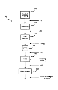
Fig. 3 is a block diagram of an OFDM modulator with SRC 300. The modulator
300 may be used as each of the modulators 130-i in the digital sub-system 100
of Fig. 1.
The input data bits from substream i are mapped to symbols Z[l] by a symbol
mapping
module 310, where 1 = 0, 1, ..., NFFT - 1 and NFFT is the number of OFDM sub-
carriers.
The precoding module 320 performs precoding of the symbols ZVI to reduce
possible out-
of-band emission. The precoded symbols are denoted as XV].
Because the interpolation for sample rate conversion at a later processing
stage in
the zmodulator 300 introduces passband droop, frequency-domain pre-distortion,
i.e. the
multiplication of XV] by a discrete frequency response H1[1], is performed by
the pre-
distortion module 330 in order to compensate for the passband droop. More
details on the
implementation of the pre-distortion filter HIM are given below. The pre-
distorted
symbols Xi[1]1-4[1] are passed to an OFDM modulation module 340, in the form
of an
Inverse Fast Fourier Transform (IFFT) module. The modulation module 340
produces a
time-domain baseband OFDM symbol xi[n], for n = 0, 1, ..., NFFT-1. The
sampling period
1
of the OFDM symbol x[n] is 7 = ____________________________________________ ,
where 4f,is the OFDM sub-carrier spacing in
Afi N FFT
= 20 the i-th frequency band.
The time-domain OFDM symbol xi[n] is then passed to a sample rate conversion
(SRC) module 350 that converts xi[n] to a baseband OFDM symbol yi[k] at the
common
sampling period T1. The SRC module 350 notionally comprises an interpolation
filter with
impulse response rri (t) that converts xi[n] into a notional continuous-time
signal xi(t),
CA 02862285 2014-07-23
WO 2012/119178 PCT/AU2011/000265
- 11 -
which is then re-sampled at the common sampling period Ti to obtain y[k] =
xi(kT1). The
purpose of the interpolation filter 6; (t) is to fulfil the anti-imaging and
anti-aliasing
requirements for SRC. More details on the implementation of the SRC module 350
are
given below.
. Finally, the sample-rate-converted baseband OFDM symbol y[k] is up-converted
by an up-conversion module 360 to a real-valued digital IF signal in the i-th
frequency
band for combining with IF signals from the other OFDM modulators in the
digital sub-
system 100 into a multiband digital IF signal.
Other types of modulators may be used as each of the modulators 130-i in the
digital sub-system 100 of Fig. 1, for example, single-carrier modulators. In a
single-carrier
modulator there is no precoding module 320, and the modulation module 340 is a
single-
carrier modulation module.
Fig. 4 is a block diagram of an OFDM demodulator with SRC 400. The
demodulator 400 may be used as each of the demodulators 220-i in the digital
sub-system
200 of Fig. 2 where the OFDM modulator 300 is in use on the transmit side. In
general,
the sample rate conversion in the OFDM demodulator 400 is a reverse operation
to that in
the corresponding OFDM modulator 300. The OFDM demodulator 400 starts with a
down-conversion module 410 that down-converts the i¨th frequency band of the
received
multiband digital IF signal with sampling period Ti to a received baseband
signal denoted
as yi[k]. The received baseband signal yi[k], also with sampling period Th is
then passed
through an SRC module 420 that converts the received baseband signal y1[k] to
a received
OFDM symbol x[n] at the sampling period Ti of the i¨th frequency band. The SRC
module 420 notionally comprises an interpolation filter with impulse response
rr, (t) that '
converts y[k] into a notional continuous-time signal yi(t), which is then re-
sampled at the
CA 02862285 2014-07-23
WO 2012/119178 PCT/AU2011/000265
- 12 -
sampling period Ti to obtain xi[n] = yi(nTi). In addition to the rejection of
image
components of the received baseband signal yi[k] in the i-th frequency band,
the
interpolation filter rr, (t) must also be able to reject signals from other
bands. More details
on the implementation of the SRC module 420 are given below.
A demodulation module 430, in the form of a Fast Fourier Transform (FFT)
module, demodulates the received OFDM symbol xi[n] to the frequency domain to
obtain a
received symbol sequence XV]. After equalisation by an equalisation module 440
and de-
precoding by a de-precoding module 450, the data symbols Z1[l] are recovered.
Finally, the
data bits in substream i are retrieved from the data symbols Z1[l] by a symbol
de-mapping
module 460.
If the modulators 130-i in the digital sub-system 100 of Fig. I are single-
carrier
modulators, so too are the demodulators 220-i in the digital sub-system 200 of
Fig. 2. In a
single-carrier demodulator there is no de-precoding module 450, and the
demodulation
module 430 is a single-carrier demodulation module that is complementary to
the single-
carrier modulation module 340.
For convenience, the same signal labels as those used in Fig. 3 are used in
Fig. 4,
but they do not necessarily refer to the same actual signals. For example,
y[k] in Fig. 4 is
the received baseband signal which includes the OFDM signal from the i-th
frequency
band as well as signal components from other bands, whereas y1[k] in Fig. 3 is
the OFDM
signal to be transmitted in the i-th frequency band only. The signal labelled
x[n] in Fig. 4
is the received OFDM signal with sampling period T, which has distortion due
to passband
droop introduced by the SRC module 420 as well as the transmission channel.
This
distortion will be somewhat compensated by the equalization module 440.
However, in
Fig. 3, xi[n] is the pre-distorted OFDM signal with sampling period
CA 02862285 2014-07-23
WO 2012/119178 PCT/AU2011/000265
- 13 -
Interpolation Filter design
The frequency spectrum of the precoded data symbols X,[1] is denoted as
X,(21) (with period 1/T1), so that X, [i] = Xi(el'firs), 1 = 0, 1, ..., NFFrl.
Also, the
frequency response of the interpolation filter r7., (t) is denoted as R? (f).
Because the
periodic spectrum Xjel2e9 comprises image components spaced at 1/Ti and the re-
sampling after interpolation will cause spectrum aliasing in the i-th
frequency band, the
interpolation filter Rri (f) is chosen so that both anti-imaging and anti-
aliasing
requirements are met. A suitable interpolation filter RT, (f) which satisfies
these
requirements is
= 47; _er
RT(f) sin ef') (1)
=
which is the product of L sinc functions.
Fig. 5 illustrates the frequency response 500 of the interpolation filter R,
(f) of
equation (1) for use in the SRC module 350 in the OFDM modulator 300 of Fig.
3. Fig. 5
also illustrates the main lobe 510 ofXi(e-12'fr' ), with bandwidth B, two of
its image
components 520, 530 centred at multiples of VT, and its NFFT samples Xi[11
spaced at Afi =
1/NFFTTi. As shown in Fig. 5, the sinc function is naturally able to reject
the image
components 520, 530 ofXi(e1247;) since the nulls of the sinc spectrum at
multiples of VT;
coincide with the centres of the image components 520, 530. The spectrum of
RT, (f) 500
rolls off in the order of f', so the interpolation filter RTi(f) of equation
(1) also offers
good anti-aliasing capability when a sufficiently large order L is selected.
However, the interpolation filter RTI(f) of equation (1) also introduces
passband
droop. That is, the magnitude of Xj[i] is attenuated more towards the two
edges of the
CA 02862285 2014-07-23
WO 2012/119178 PCT/AU2011/000265
- 14 -
main lobe 510 than at the centre of the main lobe 510 after interpolation
(equivalent to
multiplication by Rri (f)). The pre-distortion module 330 in the OFDM
modulator 300
compensates for this passband droop by multiplying X[i] by a discrete
frequency response
H1[1] that inverts the baseband frequency response of the interpolation
filter. The
frequency response Hi[I] is given by
1
for / = 0,1,= = = ¨1
RT,(1Afi)' 2
Hi[1]=
(2)
1 N N
for/ = ¨FFT +1,- , N , ¨1
((/ ¨NFFT )' 2 2 ' ¨
For the OFDM demodulator 400 of Fig. 4, the sample rate at digital IF, 1/T1,
is
much higher than the signal bandwidth B. In order to provide sufficient anti-
aliasing
ability and also reject possible unwanted signal components in addition to the
image
components of the baseband signal in the i-th frequency band from the received
and down-
converted signal y[k] (whose frequency response is denoted as Yi (e-124T1)),
the
interpolation filter rr, (t) of the SRC module 420 should have multiple nulls
in a frequency
band which has a bandwidth equal to the sample rate 1/T1. An interpolation
filter 141(f)
satisfying this requirement is also a sinc-product:
RTI (f). (NT, sin 41VT, e,
(3)
r
where M is a positive integer denoting the order of the interpolation filter
R7, (f), and N is
the number of nulls, spaced at 1/Nr1, of R, (f) within the sample rate 1/T/.
When M and
= N are properly selected, both the image components of the baseb4nd signal
in the i-th
frequency band and the unwanted components in other bands can be rejected
after
,20 interpolation.
CA 02862285 2014-07-23
WO 2012/119178
PCT/AU2011/000265
- 15 -
Fig. 6 illustrates the interpolation filter RT,(f) 600 of equation (3) for use
in the
SRC module 420 in the OFDM demodulator 400 of Fig. 4, with N set to 2. Fig. 6
also
illustrates the main lobe 610 of Yi (e)24T1), with bandwidth B, one of its
image components
620, which are centred at multiples of 1/T1, and an unwanted signal component
630. The
interpolation filter RT,(f) 600 has N = 2 mills within the sample rate 1/T1,
spaced at 1/ArT1.
The null of Rr j(f) at 1/T/ coincides with the first image component 620 of
1', (ei247.1). The
= null at 1/NT/ approximately coincides with the unwanted component 630.
The interpolation filter R, (j) according to equation (3) will also introduce
passband droop ,to the wanted signal Yi (e./2'1T' ). This passband droop, and
.any distortion
introduced by the transmission channel, is compensated by the frequency-domain
equalization module 440 in the OFDM demodulator 400.
Note that for a sinc frequency response of the form Tsin 47' e_f4 T , the time-
domain impulse response is a rectangular pulse of width T, called the gate
function gr(t),
and defined by
0 t < T
g7 (t)=(4)
0, otherwise
The product of P+1 such sinc frequency responses has a time-domain impulse
response which is the convolution of P+1 gate functions. This repeated
convolution of
P+1 gate functions is defined as the P-th order causal B-spline, denoted as
APO= gr 0)* = *
(5)
P+1
=
=
CA 02862285 2014-07-23
WO 2012/119178 PCT/AU2011/000265
- 16 -
The interpolation filters rr, (t) and rTjt) in the SRC modules 350 and 420
respectively, as defined by equations (1) and (3), may therefore be written as
A."-I) (t) and
= AV) (t) respectively.
The causal B-spline defined in equation (5) is a piecewise continuous function
oft
with pulse duration (P+1)T. An example 700 of the causal B-spline with order P
= 4 is
= illustrated in Fig. 7. Each piece of the causal B-spline is a P-th order
polynomial in t with
duration T. Suppose that the sampling period of a signal sequence to be sample-
rate-
converted is also T. If B-spline-based SRC is to be implemented directly, a
set of P+1
samples of )6';.P)(t) must be calculated and convolved with the input sequence
to generate
each output sample. Each sample of XP)(t) is a sum of up to P+1 terms, each
term being
a power of t. Direct implementation of B-spline-based SRC, like other
polynomial-based
SRC, is therefore inefficient.
Implementing devices
Disclosed below are devices configured to implement causal B-spline-based
sample rate conversion of an input signal by an arbitrary ratio. The disclosed
devices may
be used as the SRC modules 350 and 420 by appropriately setting the input and
output
sampling periods and the duration and order of the causal B-spline.
In the following, the input signal sequence with sampling period T to be
sample-
rate-converted is denoted as x(n7), the interpolated continuous-time signal as
x(t), and the
sample-rate-converted output signal sequence with sampling period T' as x(kT).
First, a device to implement sample rate conversion of x(n7) using the causal
B-
spline /ant) (single-width B-spline-based SRC) is described. The disclosed
device is
CA 02862285 2014-07-23
WO 2012/119178 PCT/AU2011/000265
- 17 -
based on the decomposition of AP (t) into a sum of P+1 normalized power
functions
t P '
p = 0, 1, ..., P. The decomposition exploits the following property of the
(
T
p-1
convolution between (¨t) g T (t) and g 1.(t):
T
t t
P-I P T
(¨T) g TO * g 7. 0=40 - Dr)(¨T) g TO + Dg TO] (6)
P
where DT denotes an operator which delays a function of t by T. Starting from
the zero-
order B-spline 41)0 = g TO , the first and second order B-splines can be
decomposed as
4) (0 = PP)(t)* gr (0 = 7' (1- DT)¨t g 7. (t)+ DT g 7.(t)1 (7)
T
using equation (6) with p = 1, and
=
2
0)(0 = OW* gT (0= T21 (1-DT ).1. (1 - DT ).(L) gT (t)
2 T
\ t / \
-1- DT =(1- DT )= --Tgr V)
+[DT = DT +(1- DT)= -I = DT"? 7. (01 (8)
- 2
using equation (7) and equation (6) with p = 2.
The above decomposition process can be continued until the P-th order B-spline
is
t P
expressed as a sum of the P+1 normalized power functions -:- g 7. (I), p = 0,
...,P, each
(
T
of which is multiplied by a composite operator composed of a series of DT and
1-Dr. .
To reconstruct the signal x(t) using the decomposed P-th order B-spline, each
composite operator is applied to the input sequence x(n7), with the operator
DT -
implemented by a delay element 11 and the operator 1-Dr by a delay-difference
element
CA 02862285 2014-07-23
WO 2012/119178
PCT/AU2011/000265
- 18 - =
= 1-z-1. The resulting intermediate sequence, denoted as vp(nT), is then
convolved with the
corresponding normalized power function. The interpolated signal x(t) may
therefore be
written as
L,
P =
x(t)=EP vp(nT)*(¨t) gr(t)
(9)
p=0 T
The P+1 intermediate sequences vp(nT), collectively denoted as a state vector
v(n T) = [v0(nT),v1(nT),= = = ,v p(nT)1, can be efficiently obtained through a
discrete delay
and difference network according to the above decomposition process. The
number of
multiplications required in the (P+1)-output delay and difference network is
only (P-1 )P/2. =
Since each intermediate sequence vp(nT) from the delay and difference network
has sampling period 7', and the duration of the corresponding normalized power
function
P
1 j gr
(0 is also T, the interpolated signal x(t) in the interval [nT,(n +1)T) is
given by
(
T
P
= x(t) = E vP (nT)(t ¨T nT)P g T 1, it ¨ nT)
(10)
p=0
without any overlapping of adjacent normalized power functions.
To re-sample the interpolated signal x(t) at sampling period T' to produce the
k-th
output sample x(kr), first define the k-th integer index m(k) and the k-th
fractional
,
interval ,u(k) E [OA as follows: .
.
kT' =[m(k)+ AkAT
(11)
Using the terms defined in equation (11), the re-sampling of x(t) at sampling
= period T'
according to equation (10) becomes ,
P =
= x(kT')= E v p(m(k)TX14(k))P (12)
p=0
Equation (12) has an equivalent, nested form
CA 02862285 2014-07-23
WO 2012/119178 PCT/AU2011/000265
- 19 -
= x(kT') = ((= = = ( vp (m(k)T)p(k)+
(m(k)T) )/./(10+ vo (m(k)r) (13)
which comprises the P-fold iteration of a primitive comprising a
multiplication of the
intermediate sequence vp(m(k)T) by p(k) followed by an addition of the next
intermediate
sequence vp_1(m(k)T). Thus the total number of multiplications required to
implement
Equation (13) is (P+1)P/2, which is half the (P+1)P multiplications in the
conventional
Farrow structure. =
Fig. 8 illustrates a device 800 for single-width causal-B-spline-based sample
rate
conversion, based on Equation (13). The SRC device 800 may be used as the SRC
module
350 in the OFDM modulator 300 of Fig. 3 by setting T = Ti, T' = T1, and P = L-
1. The
value of L depends on the stopband attenuation requirement. For example, if 50
dB
attenuation is required, L is set to 5. Each element marked "II", e.g. 810,
implements the
delay operator DT used in equation (6) to define the intermediate sequences
vp(n7). To the
left of the vertical line 820 lies the discrete delay and difference network
used to produce
the intermediate sequences vp(nT). To the right of the vertical line 820 is a
ladder structure
830 comprising successive multiplication-addition elements that implement the
nested
structure of equation (13).
The index m(k) and the fractional interval ,u(k) are both initialised to 0 for
k = 0,
then iteratively updated for each successive value of k as follows:
= m(k
+1) = m(k)+ floor(p(k)+ ¨7") (14)
7.1 =
,u(k +1)= ,u(k)+ ¨7" floor(p(k)+ --) (15)
CA 02862285 2014-07-23
WO 2012/119178 PCT/AU2011/000265
- 20 -
Now, a device to implement sample rate conversion of the input sequence x(n7)
to
an output sampling period of T' using the causal B-spline fig? (t) (multi-
width B-spline-
based SRC) is described. .
Following the same procedure as described above, the causal B-spline fig.)(t)
can
be decomposed into a sum of P+1 normalized power functions .
t P
--:-.- g Nr(t), p = 0,1,..., P. Since these normalized power functions have
pulse duration
(
NT
NT, whereas the input sequence x(n7) has a sampling period T, the contribution
to the
P
interpolated signal x(t) by each normalized power function ¨t
gwr (t) in the interval
(
NT
[n7', (n +1)T) will be a sum of N overlapped normalized power functions, i.e.
P N-1 P i .
x(t)= EE vp (nT ¨ iT)(t+iT¨nT) g k
NTt + 1T ¨ nT),t e [nT,(n +1)T)
(16)
p=0 i=0 NT .
where v(n7) is the p-th element of the state vector v(nT) obtained by a delay
and
difference network similar to that illustrated in Fig. 8, but with N-sample
delay elements
z-N and delay-and-difference elements 1-1N.
Using the terms defined in equation (11), the re-sampling of the interpolated
signal x(t) at sampling period T' according to equation (16) becomes
N-1 P
X(ICT1)= EEvpqm(k)¨ 071(140+ i)P
(17)
i=0 p=0 N )
,
The k-th sample x(kr) may then be calculated, by analogy with the nested
equation (13) above, as
=
N-1
*71= E ((= = = ( vpqm(k)-0T)P(k)-f-i +...v,qm(k) 0T) )P(k)+' + vo((m(k)¨ 0T)
N N
P
(18)
_
=
CA 02862285 2014-07-23
WO 2012/119178 PCT/AU2011/000265
- 21 -
Fig. 9 illustrates an device 900 for multi-width causal B-spline-based sample
rate
conversion, based on Equation (18). The SRC device 900 may be used as the SRC
module.
420 in the OFDM demodulator 400 of Fig. 4 by setting T = T1, T' = T1, P = M-1,
and an
appropriate N. The values of M and N depend on how many unwanted signal
components
. 5 need to be nulled and the stopband attenuation requirement. For
example, if the IF image
signal component is to be nulled and the required stopband attenuation is 50
dB, the chosen
values are N=2 and M=4. The SRC device 800 is a special case of the device
900, with N
set to 1.
To the left of the vertical line 920 lies the discrete delay and. difference
network
used to derive the intermediate sequences vp(nT), which is the same as the
delay and
. difference network in the device 800 of Fig. 8, but with the delay
elements 11 replaced by
N-sample delay elements IN. To the right of the vertical 1ine-920 are N ladder
structures,
e.g. 930, comprising successive multiplication-addition elements that
implement the nested
structure of the summed terms in equation (18). The outputs of the N ladder
structures are
added together to produce the output sequence x(kr).
Figs. 10A and 10B collectively form a schematic block diagram of an embedded
computing device 1001, in which the SRC modules 350 and 420 may alternatively
be
implemented. As seen in Fig. 10A, the electronic device 1001 comprises an
embedded
controller 1002. Accordingly, the electronic devic.e 1001 may be referred to
as an
"embedded device." The controller 1002 has a processing unit (or processor)
1005 which .
is bi-directionally coupled to an internal storage module 1009. The storage
module 1009
may be formed from non-volatile semiconductor read only memory (ROM) 1060 and
semiconductor random access memory (RAM) 1070, as seen in Fig. 10B. The RAM
1070
may be volatile, non-volatile or a combination of volatile and non-volatile
memory.
CA 02862285 2014-07-23
WO 2012/119178 PCT/AU2011/000265
- 22 -
As seen in Fig. 10A, the electronic device 1001 also comprises a portable
memory
interface 1006, which is coupled to the processor 1005 via a connection 1019.
The
portable memory interface 1006 allows a complementary portable computer
readable
storage medium 1025 to be coupled to the electronic device 1001 to act as a
source or
destination of data or to supplement the internal storage module 1009.
Examples of such
interfaces permit coupling with portable computer readable storage media such
as
Universal Serial Bus (USB) memory devices, Secure Digital (SD) cards, Personal
Computer Memory Card International Association (PCMIA) cards, optical disks
and
magnetic disks.
The electronic device 1001 also has a communications interface 1008 to permit
coupling of the electronic device 1001 to a computer or communications network
1020 via
a connection 1021. The connection 1021 may be wired or wireless. For example,
the
connection 1021 may be radio frequency or optical. An example of a wired
connection
includes Ethernet. Further, an example of wireless connection includes
BluetoothTm type
local interconnection, Wi-Fi (including protocols based on the standards of
the IEEE
802.11 family), Infrared Data Association (IrDa) and the like.
The methods described hereinafter may be implemented using the embedded
controller 1002, as one or more software application programs 1033 executable
within the
embedded controller 1002. In particular, with reference to Fig. 10B, the steps
of the
described methods are effected by instructions in the software 1033 that are
carried out
within the embedded controller 1002. The software instructions may be formed
as one or
more code modules, each for performing one or more particular tasks.
The software 1033 of the embedded controller 1002 is typically stored in the
non-
volatile ROM 1060 of the internal storage module 1009. The software 1033
stored in the
ROM 1060 can be updated when required from a computer readable medium. The
CA 02862285 2014-07-23
WO 2012/119178 PCT/AU2011/000265
-.23 -
software 1033 can be loaded into and executed by the processor 1005. In some
instances,
the processor 1005 may execute software instructions that are located in RAM
1070.
Software instructions may be loaded into the RAM 1070 by the processor 1005
initiating a
copy of one or more code modules from ROM 1060 into RAM 1070. Alternatively,
the
The application program 1033 is typically pre-installed and stored in the ROM
In another alternative, the software application program 1033 may be read by
the
processor 1005 from the network 1020, or loaded into the embedded controller
1002 from
CA 02862285 2014-07-23
WO 2012/119178 PCT/AU2011/000265
- 24 -
computer readable transmission media that may also participate in the
provision of
software, application programs, instructions and/or data to the electronic
device 1001
include radio or infra-red transmission channels as well as a network
connection to another
computer or networked device, and the Internet or Intranets including e-mail
transmissions
Fig. 1013 illustrates in detail the embedded controller 1002 having the
processor
1005 for executing the application programs 1033 and the internal storage
1009. The
internal storage 1009 comprises read only memory (ROM) 1060 and random access
memory (RAM) 1070. The processor 1005 is able to execute the application
programs
The processor 1005 typically includes a number of functional modules including
a
control unit (CU) 1051, an arithmetic logic unit (ALU) 1052 and a local or
internal
memory comprising a set of registers 1054 which typically contain atomic data
elements
1056, 1057, along with internal buffer or cache memory 1055. One or more
internal buses
The application program 1033 includes a sequence of instructions 1062 though
1063 that may include conditional branch and loop instructions. The program
1033 may
CA 02862285 2014-07-23
WO 2012/119178 PCT/AU2011/000265
- 25 -
as part of the instruction or in a separate location 1064 within the ROM 1060
or RAM
1070.
In general, the processor 1005 is given a set of instructions, which are
executed
therein. This set of instructions may be organised into blocks, which perform
specific
tasks or handle specific events that occur in the electronic device 1001.
Typically, the
application program 1033 waits for events and subsequently executes the block
of code
associated with that event. Events may be triggered in response to input from
a user, via
the user input devices 1013 of Fig. 10A, as detected by the processor 1005.
Events may
also be triggered in response to other sensors and interfaces in the
electronic device 1001.
The execution of a set of the instructions may require numeric variables to be
read
and modified. Such numeric variables are stored in the RAM 1070. The disclosed
method
uses input Variables 1071 that are stored in known locations 1072, 1073 in the
memory
1070. The input variables 1071 are processed to produce output variables 1077
that are
stored in known locations 1078, 1079 in the memory 1070. Intermediate
variables 1074
may be stored in additional memory locations in locations 1075, 1076 of the
memory 1070.
Alternatively, some intermediate variables may only exist in the registers
1054 of the
processor 1005.
The execution of a sequence of instructions is achieved in the processor 1005
by
repeated application of a fetch-execute cycle. The control unit 1051 of the
processor 1005
maintains a register called the program counter, which contains the address in
ROM 1060
or RAM 1070 of the next instruction to be executed. At the start of the fetch
execute cycle,
the contents of the memory address indexed by the program counter is loaded
into the
= control unit 1051. The instruction thus loaded controls the subsequent
operation of the
processor 1005, causing for example, data to be loaded from ROM memory 1060
into
processor registers 1054, the contents of a register to be arithmetically
combined with the
=
CA 02862285 2014-07-23
WO 2012/119178 PCT/AU2011/000265
- 26 - =
contents of another register, the contents of a register to be written to the
location stored in
another register and so on. At the end of the fetch execute cycle the program
counter is
updated to point to the next instruction in the system program code. Depending
on the
instruction just executed this may involve incrementing the address contained
in the
program counter or loading the program counter with a new address in order to
achieve a -
branch operation.
Each step or sub-process in the ,processes of the methods described below is
associated with one or more segments of the application program 1033, and is
performed
by repeated execution of a fetch-execute cycle in the processor 1005 or
similar
programmatic operation of other independent processor blocks in the electronic
device
1001.
The arrangements described are applicable to the digital communication
industries.
The foregoing describes only some embodiments of the present invention, and
modifications and/or changes can be made thereto without departing from the
scope and
spirit of the invention, the embodiments being illustrative and not
restrictive.