Note: Descriptions are shown in the official language in which they were submitted.
CA 02862975 2014-07-09
WO 2013/104051
PCT/CA2013/000012
VITAL DIGITAL INPUT
Field of the invention
[01] The invention relates to digital input circuits, and more particularly to
circuits with high immunity to induced AC noise in the input signal.
Background of the invention
[02] In a digital input interface a DC signal from a remote unit arrives over
a
signal line. The voltage of the DC signal is used to determine whether a
digital
"1" or a "0" is to be sent to other subsystems. At its most basic, a Zener
diode
can be used in series with a resistor and a current detector. If the DC
voltage is
high enough that it exceeds the breakdown voltage of the Zener diode then a
current flows through the circuit, and the current detector indicates that the
DC
signal is active. If the DC voltage is lower than the breakdown voltage of the
Zener diode then no current flows through the circuit, and the lack of current
induces the current detector to indicate that the DC signal is inactive.
[03] For example, rail systems usually have a control system for managing
trains. The control system receives state information from remote field
elements. Some remote field elements provide this information to the control
system by setting the DC voltage on a wire leading to the control system. At
the
control system the voltage on the wire is used to establish the state of the
device
to which the respective field element is assigned.
[04] As a simple example, a railroad track circuit is given. To manage train
traffic, the track is divided in segments called blocks. When a block is
occupied
by a train, the track circuit detects the presence of the train and signals to
the
control systems using a DC voltage. At the control system, the voltage on the
1
CA 02862975 2014-07-09
WO 2013/104051
PCT/CA2013/000012
wire is detected and used to transmit to subsystems a digital indication of
the
block occupancy. A diagram of such a system is shown in FIG. 1. The track
circuits are always constructed in such way that it will signal "low" or OV if
a
train is detected and "high" or 24V (for example) if the block is not
occupied.
The "high" or active state is called "permissive" in this context because in
this
state the trains are permitted to enter the block. Opposite, the "low" state
is
called "restrictive" because trains are restricted from entering the track
block.
[05] The signaling method based on permissive/restricted concept described
for the track circuit is also applied for other system elements such as train
and
platform doors, rail switches, trip stop mechanisms, etc. In general, the
permissive state is always associated with electrical elements/circuits being
in
an energized state. With this signaling arrangement, failures such as
interrupted wires or bad circuit contacts will always result in "low" signals.
In
such case traffic will be restricted (stopped) and therefore the possible
failure
will always result in a safe state.
[06] A digital input interface is termed "vital" if 100% certainty is needed
in
asserting the "permissive" or "1" or "high" state, and by corollary it must be
known if the interface is faulty in such a way that the fault may indicate a
"permissive" ("1") state when the input signal signals in fact a "restrictive"
("0"). Digital input interfaces for rail control systems are often vital. In
the
example given above, it is crucial that the subsystems correctly know the
unoccupied state of the block. An incorrect reading resulting from an
unknowingly faulty interface can have disastrous consequences, such as
allowing another train to enter the block when the control subsystem
erroneously interprets an input signal as "permissive" when in fact the input
signal is meant to be read as "restrictive". It is however acceptable from a
safety
perspective that the digital input interface may fail in such a way that it
will
indicate a state of "restrictive" when in fact the field element indicates
"permissive". This type of failure is still undesirable because it will cause
trains
2
CA 02862975 2014-07-09
WO 2013/104051
PCT/CA2013/000012
to stop unnecessarily with consequences in delays and revenue, but at least no
accidents will happen.
[07] One cause of error is induced noise. Nearby electrical wires can induce
an AC signal in the DC signal sent from the remote field element to the
interface. For example, the signal line from a field element to the control
system
in railroad systems usually lies along a railroad track. Due the distance
between the field element and the control system, which is often at a central
location, there is a good chance that the signal line will pass near other
electrical
wires. The induced AC noise can bring the received voltage above the
threshold in a periodic manner. This, in conjunction with the read-by-sampling
of the input processor can result in an assignment of a "1" as if a valid DC
signal were received. An example of this is illustrated in FIG. 2.
[08] Another cause of error is the decay of the threshold to which the DC
voltage is compared in order to determine of the input signal corresponds to a
"1" or a "0". This can occur as the characteristics of circuit components
change
with age or temperature. Manufacturing issues, environmental conditions, or
electrical surges may also produce failure in circuits and components. For
example, the breakdown voltage of a Zener diode may gradually change with
time, or altematively the reverse leakage current can increase. This can
exacerbate the effects of noise, as following such events low magnitude noise
may falsely trigger the input circuit into the "high" state.
[09] Yet another possible cause of error is the asymmetry of the input
circuit.
Common mode noises may be transformed into differential mode noises,
contributing to false triggering of the input circuit into the "high" state.
[10] An interface which minimized the effect of noise would contribute to the
vitality of the interface, as would periodic test for detection of threshold
decay
and noise attenuation capability.
3
CA 02862975 2014-07-09
WO 2013/104051
PCT/CA2013/000012
Summary of the invention
[111 In accordance with one aspect of the invention, a digital input interface
circuit is provided. The digital input interface has a line carrying an input
signal, and a first optocoupler, a first resistor, and a second resistor,
connected
in series on the line. A capacitor is connected in parallel with the first
optocoupler and connected in series with the first resistor and with the
second
resistor. A Zener diode and at least one additional optocoupler are connected
in
series, the Zener diode and the at least one additional optocoupler being
connected in parallel with the capacitor, being connected in parallel with the
first optocoupler, and being connected in series with the first resistor and
with
the second resistor. Each additional optocoupler has a corresponding input
processor configured to receive electrical signals from a receiving side of
the
optocoupler. A Latent Failure Detection (LFD) engine is configured to receive
signals from the least one input processor and is configured to send signals
to
open and close the first optocoupler, whereby in response to commands from
one of the at least one input processor the LFD engine is able to send signals
to
the first optocoupler causing the first optocoupler to close for a
predetermined
duration and then open. Each input processor is configured to determine a
response time of the capacitor from signals received from the corresponding
additional optocoupler. Each input processor is configured to determine that
the digital input interface is unreliable if the input processor determines
that the
response time of the capacitor falls outside a predetermined range.
[12] In accordance with another aspect of the invention, a method of
determining the reliability of a digital input interface is provided. A first
optocoupler on the interface is closed for a predetermined duration, causing
current to bypass at least one additional optocoupler. After the predetermined
duration the first optocoupler is opened, causing the capacitor to charge and
after a period of time causing current to flow through the additional at least
one
optocoupler because of breakdown of a Zener diode when the capacitor is
4
CA 02862975 2014-07-09
WO 2013/104051
PCT/CA2013/000012
sufficiently charged. For each additional optocoupler, a response time is
determined as the difference in time between opening of the first optocoupler
and an indication by the additional optocoupler that current is flowing
therethrough. If any determined response time is outside a predetermined
range of an expected response time, then it is determining that the digital
input
interface is unreliable.
[13] In accordance with yet another aspect of the invention, a digital
input interface circuit is provided. The digital input interface has a line
carrying
an input signal, a first optocoupler cormected in series on the line, a
capacitor
connected in parallel with the first optocoupler, at least one voltage
threshold
circuit, at least one input processor, each input processor corresponding to
one
of the at least one voltage threshold circuit, and a Latent Failure Detection
(LFD)
engine configured to send signals to open and close the first optocoupler.
Each
input processor is configured to determine a response time of the capacitor
from
signals received from the corresponding voltage threshold circuit. Each input
processor is configured to determine that the digital input interface is
unreliable
if the input processor determines that the response time of the capacitor
falls
outside a predetermined range.
[14] The interface of the present invention allows a high impedance for the
DC input signal and a low impedance for induced AC noise. Since non-
intended AC coupling implies a high source impedance, any AC induced noise
will be naturally attenuated. The interface also provides a latent failure
detection engine which can be used to periodically check for threshold decay
by
determining the charging time of a capacitor in the signal side of the
interface.
An added advantage is that the circuit forms a natural filter blocking higher
frequency signals, and therefore the sampling frequency can be lower without
risking the aliasing effects illustrated in FIG. 2.
CA 02862975 2014-07-09
WO 2013/104051
PCT/CA2013/000012
Brief description of the drawings
[151 The features and advantages of the invention will become more apparent
from the following detailed description of the preferred embodiment(s) with
reference to the attached figures, wherein:
FIG. 1 is a diagram of an example field element;
FIG. 2 is a timing diagram showing an aliasing effect;
FIG. 3 is a circuit diagram of a digital input interface according to one
embodiment of the invention;
FIG. 4 is a timing diagram showing the relationship between LFD pulse
width and capacitor response in the circuit of FIG. 3 according to one
embodiment of the invention; and
FIG. 5 is a circuit diagram of a digital input interface according to
another embodiment of the invention.
[16] It will be noted that in the attached figures, like features bear similar
labels.
Detailed description of the embodiments
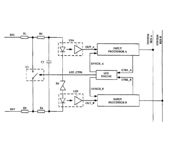
[171 Referring to FIG. 3, a circuit diagram of a digital input interface
according to one embodiment of the invention is shown. The interface
comprises an input side connected to a remote field element (the left side of
FIG. 3) and an output side connected to a control system (the right side of
FIG.
3). On the input side, the line carrying the signal SIG contains in series a
first
resistor R1, a first optocoupler U1, and a second resistor R2. In parallel
with the
first optocoupler U1 are a third resistor R3, a non-polarized capacitor C1,
and a
6
CA 02862975 2014-07-09
WO 2013/104051
PCT/CA2013/000012
fourth resistor R4, all in series. In parallel with the capacitor C1 are a
second
optocoupler U2A, a zener diode D1, and a third optocoupler U2B, all in series.
[18] The first optocoupler U1 acts like an open-closed switch, as explained
below, and hence is shown as a switch in FIG. 3. The emitting side of the
first
optocoupler U1 (that coming from the output side) is an LED. Examples of
suitable implementations of the receiving side of the first optocoupler U1
(that
is, on the input side of the interface) are a phototransistor bipolar, a
phototransistor bipolar Darlington, and a phototransistor MOS.
[19] The second and third optocouplers U2A and U2B have LEDs on the
input side. Examples of suitable implementations of the photodetector on the
receiving side (that is, on the output side of the interface) are a
photodiode, a
phototransistor bipolar, a phototransistor bipolar Darlington, and a
phototransistor MOS.
[20] On the output side the photodetector within the second optocoupler U2A
is triggered by photons from the LED of the second optocoupler U2A and
produces electrical signals, the second optocoupler U2A having a first
activation
level. The second optocoupler U2A is coupled to and feeds electrical signals
OUT_A to a first input processor A. The first input processor A is coupled to
a
first system bus. The first input processor A is also coupled to and can send
control signals to a Latent Failure Detection (LFD) engine. The LFD engine can
send LFD control signals to the first optocoupler U1. The LFD engine is also
coupled to and can send synchronization signals to the first input processor
A.
Collectively, the first input processor A and the first system bus are termed
herein as the first output subsystem.
[21] The photodetector within the third optocoupler U2B is triggered by
photons from the LED of the second optocoupler U2B and produces electrical
signals, the third optocoupler U2B having a second activation level. The third
optocoupler U2B is coupled to and feeds electrical signals OUT_B to a second
7
CA 02862975 2014-07-09
WO 2013/104051
PCT/CA2013/000012
input processor B. The second input processor B is coupled to a second system
bus. The second input processor B is also coupled to and can send control
signals to the L1-t) engine. The LFD engine is also coupled to and can send
synchronization signals to the second input processor B. Collectively, the
second input processor B and the second system bus are termed herein as the
second output subsystem. The second output subsystem is a duplication of the
first output subsystem.
[221 The use of the optocouplers U1, U2A, and U2B electrically isolates the
input side of the interface from the output side of the interface. This
protects
the processors on the output side against field impairments such as electrical
surges and inductions.
[231 In operation, the first optocoupler U1 is normally left open. The voltage
of the signal SIG produces a current which charges the capacitor C1 and
attempts to pass through the zener diode D1. If SIG is of a high voltage then
the
capacitor C1 will quickly charge, and the breakdown voltage of the Zener diode
D1 is set so that the high voltage of SIG causes current to flow through the
LEDs
of the optocouplers U2A and U2B. The LEDs then produce photons which
reach the photodetectors of the optocouplers U2A and U2B and, assuming the
activation levels of the photodetectors is exceeded, signals are sent to the
respective input processor. The input processors indicate to the respective
system bus that a high binary state has been indicated by SIG.
[241 If the signal SIG is of a low voltage then the breakdown voltage of the
Zener diode is not reached, no or very little current passes through the LEDs
of
the optocouplers U2A and U2B, the photodetectors of the optocouplers U2A
and U2B are not triggered, no or very low power signals are sent to the
respective input processor, and the input processors indicate to the
respective
system bus that a low binary state has been indicated by the signal SIG.
8
CA 02862975 2014-07-09
WO 2013/104051
PCT/CA2013/000012
[251 The capacitor Cl in series with the resistors acts to filter high
frequencies
in the signal SIG. This lowpass filter blocks out high frequency components of
any AC noise in the signal SIG. The lowpass filter also prevents any high
frequencies which could otherwise lead to aliasing, which allows a lower
sampling frequency of the signal SIG to be used.
[26] Periodically the system is tested for threshold decay. This is done by
closing and opening the first optocoupler U1. When this is done, the capacitor
C1 recharges and there is some delay before the voltage across the Zener diode
D1 reaches the breakdown voltage, at which point the photodiodes of the
optocouplers U2A and U2B are triggered. Referring to FIG. 4, a timing diagram
showing the relationship between LFD pulse width and capacitor response in
the circuit of FIG. 3 according to one embodiment of the invention is shown.
The periodic testing is performed when the voltage of the input signal V(SIG)
is
high. During a particular test the voltage of the input signal V(SIG) may be
low,
or may start low and switch to high mid-test, but in either case that
particular
test is simply ignored.
[271 The capacitor C1 has a response time for the voltage across the capacitor
V(C1) to reach a threshold. At this point, since the first optocoupler U1 is
left
open, the breakdown voltage of the Zener diode D1 is reached and the
photodiode of the second optocoupler U2A is triggered, and the first input
processor A receives a high output value OUT_A. The photodiode of the third
optocoupler U2B is also triggered, causing the second input processor B to
also
read a high output value OUT_B, but this is not shown in FIG. 4.
[28] The first input processor A then sends a CTRL signal to the LFD Engine.
In response thereto, the LFD Engine sends a synchronization signal to each
input processor, and then sends an LFD_CTRL signal of duration LFD_PW.
The LFD_CTRL signal causes the first optocoupler U1 to close. The input signal
SIG travels through the resistors R1, R2, and the closed optocoupler U1, and
the
9
CA 02862975 2014-07-09
WO 2013/104051
PCT/CA2013/000012
capacitor C1discharges. The drop in V(C1) causes the voltage across the Zener
diode D1 to fall below the breakdown voltage. The first input processor A and
the second input processor B receive low output values OUT_A and OUT_B
since current bypasses the second and third optocouplers U2A and U2B and
there insufficient current therethrough to trigger output of photons.
[29] After the duration LFD_PW, the LFD Engine stops sending the
LFD_CTRL signal and the first optocoupler U1 opens. The charge on the
capacitor C1 increases, and after a duration XT the voltage across the
capacitor
V(C1) again exceeds the threshold necessary to trigger the photodiodes in the
optocouplers U2A and U2B, and the first input processor A and the second
input processor B receive high output values OUT_A and OUT_B.
[30] It should be noted that only one of the two input processors send a CTRL
signal to the LFD Engine to trigger a LFD_CTRL signal. However both input
processors determine the value of XT, which is a measure of the response time
of the capacitor C1. As stated above, after receiving a CTRL signal from
either
input processor, the LFD Engine sends a synchronization signal to each input
processor. Upon receiving a synchronization signal from the LFD Engine, each
input processor enters a WAIT mode. When an input processor enters a WAIT
mode it expects to acquire two events: OUT_A (or OUT_B) falling from "1" to
"0", followed by OUT_A (or OUT_B) rising from "0" to "1". Each input
processor has the capability to measure the time elapsed between these two
events. The length of LFD_PW is known to each input processor, and the
measured value of XT can be determined by subtracting the known duration of
LFD_PW from the total time measured between the two events.
[31] In one embodiment, analysis of the two values of XT determined by the
input processors is done by the input processors themselves. The input
processors each send its respective measured value of XT to the other input
processor using a protocol over a local link (not shown in FIG. 3). Each input
CA 02862975 2014-07-09
WO 2013/104051
PCT/CA2013/000012
processor compares the received value of XT with its own measured value of
XT. If either input processor determines that the two measured values of XT
are
not identical (or close within acceptable tolerance) then that input processor
reports the health of the input circuit as "FAILED", i.e. the digital input
interface is unreliable.
[32] If the input processors determine that the two measured values of XT are
identical (or close within acceptable tolerance) then the interface is itself
evaluated by comparing the measured value of XT with an expected value of
XT. The effects of threshold decay can be seen by considering FIG. 4. As the
threshold above which a "1" is determined lowers, the time at which V(C1)
crosses the threshold following re-opening of the first optocoupler U1
shortens.
Some deviation from the expected value of XT is expected, for example due to
allowed variance in the voltage of an "on" signal SIG. However, if an input
processor determines that the measured value of XT is outside a predetermined
acceptable range of the expected value of XT, then the threshold has decayed
and the input processor reports the health of the input circuit as "FAILED".
[33] In an alternative embodiment, analysis of the two values of XT
determined by the input processors is done at a higher system level (not shown
in FIG. 3). The input processors each send its respective measured value of XT
over the respective system bus to the next higher system. The higher system
compares the received measured values of XT. If the higher system determines
that the two measured values of XT are not identical (or close within
acceptable
tolerance) then the higher system evaluates the health of the input circuit as
"FAILED". If the higher system determines that the two measured values of XT
are identical (or close within acceptable tolerance) then the interface is
itself
evaluated by comparing the measured value of XT with an expected value of
XT. If the higher system determines that the measured value of XT is less than
the expected value of XT, then the threshold has decayed and the higher system
evaluates the health of the input circuit as "FAILED".
11
CA 02862975 2014-07-09
WO 2013/104051
PCT/CA2013/000012
[34] In either embodiment, the input circuit is deemed to be good only if the
measured values of XT are the same and if the measured value of XT is close to
the expected value of XT.
[35] The value of XT is determined by both input processors in order to
provide the level of trust required by the vital concept. In other words, two
processors measuring the same parameter should produce the same, or
practically the same, result. A simultaneous failure in both input processors
in
such a way that both would measure XT with significant and identical error is
extremely unlikely.
[36] The interface disclosed provides additional advantages in reducing
induced noise. The input interface consists of a symmetrical circuit (R1, R2,
R3,
R4, and C1). The non-symmetrical components (the Zener diode D1 and the
LEDs of the optocouplers U2A and U2B) are behind the symmetrical structure.
This arrangement offers maximum common mode noise immunity.
[37] Induced AC noise is also reduced by selecting the values of R1, R2, and
the capacitance of C1 so as to increase impedance at low frequencies and
decrease impedance at high frequencies. The signal perceived at the input of a
circuit is, ignoring the normal signal source in the circuit, the noise
magnitude
VN reduced by a factor of input impedance divided by the sum of input
impedance ZIN and noise impedance ZN
[38] ViN = VN * (ZIN (ZIN ZN) ).
[39] It is therefore desirable for an input circuit to have a low input
impedance at frequencies at which AC inductions may occur. However, in
order to minimize the useful DC signal attenuation and power dissipation and
to ensure a reasonable response time, it is desirable for the circuit to have
a
rather high impedance at very low frequencies, including DC.
12
CA 02862975 2014-07-09
WO 2013/104051
PCT/CA2013/000012
[40] Referring to FIG. 5, an alternative in which there are two input circuit
interfaces is shown. Each input circuit interface is identical, and is similar
to
that shown in FIG. 3 except each input circuit interface has only one
optocoupler producing signals. Each input processor measures the value of XT
of each output optocoupler. This circuit arrangement allows variations of XT
due to normal conditions such as input voltage variations and temperature to
be better distinguished from variations of XT due to failure or circuit
degradation.
[41] The embodiments described above measure XT by sending a single pulse
LFD_CTRL from the LW Engine to the first optocoupler U1. Alternatively, the
LFD Engine sends a succession of pulses of various durations. This allows
better precision in evaluating XT.
[42] The embodiments described above have an LFD Engine as a device
separate from the input processors. Alternatively, the LFD Engine can be
implemented within the same devices as the input processor.
[43] The functionality of the LFD Engine and the input processors described
above are preferably carried out by circuitry within integrated chips.
Alternatively, any form of hardware could be used to carry out the
functionality
of the LFD Engine and the input processors, as could software or any
combination of hardware and software. If carried out in whole or in part by
software, the software can be stored as instructions on a non-transitory
computer-readable storage medium.
[44] The invention has been described using a Zener diode and optocouplers
U2A and U2B as voltage threshold circuits for detecting if an input voltage
exceeds a threshold. Alternatively, any other embodiment of one or more
voltage threshold circuits may be used, such as a comparator. Two or more
voltage threshold circuits may share one or more components, such as the
Zener diode in the embodiment described above.
13
CA 02862975 2014-07-09
WO 2013/104051
PCT/CA2013/000012
[45] The embodiments presented are exemplary only and persons skilled in
the art would appreciate that variations to the embodiments described above
may be made without departing from the spirit of the invention.
14