Note: Descriptions are shown in the official language in which they were submitted.
77846-45
SENSOR CIRCUIT FOR CONTROLLING, DETECTING, AND MEASURING A
MOLECULAR COMPLEX
CROSS REFERENCE TO OTHER APPLICATIONS
[0001] This application claims priority to U.S. Provisional Patent
Application No.
61/603,782 entitled SENSOR CIRCUIT FOR CONTROLLING, DETECTING, AND
MEASURING A MOLECULAR COMPLEX filed February 27, 2012.
BACKGROUND OF THE INVENTION
[0002] Advances in micro-miniaturization within the semiconductor
industry in recent
years have enabled biotechnologists to begin packing traditionally bulky
sensing tools into
smaller and smaller form factors, onto so-called biochips. It would be
desirable to develop
techniques for biochips that make them more robust, efficient, and cost-
effective.
SUMMARY OF THE INVENTION
[0002a] According to one aspect of the present invention, there is
provided a device
comprising: a plurality of measurement cells, each measurement cell including
a cell
electrode above which a nanopore is formed, the cell electrode configurable to
apply a distinct
potential that is independent from cell electrodes in other measurement cells,
each
measurement cell including an integrator electronically coupled to the cell
electrode; a
common electrode, the common electrode configured to apply a common potential
to a liquid
above the nanopores formed above the cell electrodes in the plurality of
measurement cells,
wherein the common potential is common to all of the measurement cells, and
wherein the
integrator in each measurement cell measures a current flowing between the
common
electrode and the cell electrode in the measurement cell; a plurality of
analog-to-digital
converters, wherein one of the integrators from the plurality of measurement
cells is
electrically coupled to one analog-to-digital converter of the plurality of
analog-to-digital
converters.
1
CA 2863211 2018-01-15
77846-45
[0002b] According to another aspect of the present invention, there is
provided an electric
circuit for applying a voltage while simultaneously measuring a current
flowing between a
common electrode and cell electrodes, the electric circuit comprising: a
plurality of cell
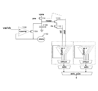
electrodes, wherein a nanopore may be formed above each cell electrode, and
wherein each
electrode is located in one of a plurality of measurement cells, each
electrode is configurable to
apply a distinct potential that is independent from cell electrodes in other
measurement cells; a
common electrode, the common electrode configured to apply a common potential
to a liquid
above the nanopores formed above the cell electrodes in the plurality of
measurement cells,
wherein the common potential is common to all of the measurement cells; for
each cell electrode
of the plurality of cell electrodes, an integrator electronically coupled to
the cell electrode, the
integrator including an integrating capacitor, wherein a voltage across the
integrating capacitor
comprises a measure of the current flowing between the common electrode and
the cell electrode
during a measurement period.
BRIEF DESCRIPTION OF THE DRAWINGS
[0003] Various embodiments of the invention are disclosed in the following
detailed
description and the accompanying drawings.
[0004] Figure 1 illustrates a single stranded DNA (ssDNA) molecule
constrained in a
nanopore in a cell 100.
[0005] Figure 2 illustrates an embodiment of a cell 200 performing
nucleotide sequencing
with the nanopore-based sequencing by synthesis (Nano-SBS) technique.
[0006] Figure 3 illustrates four physical states of a sensor cell.
[0007] Figure 4 illustrates an embodiment of a bank (M x N) of cells.
[0008] Figure 5 illustrates a 128k array implemented as sixteen bank8k
elements.
[0009] Figure 6 illustrates a 512k array implemented as an 8x8 array
of bank8k elements.
[0010] Figure 7 illustrates an embodiment of a bank8k block.
[0011] Figure 8 illustrates an embodiment of a scan sequence.
la
CA 2863211 2018-01-15
CA 02863211 2014-07-29
WO 2013/130635 PCT/US2013/028058
[0012] Figure 9 illustrates an embodiment of a scan sequence.
[0013] Figure 10 illustrates that a fraction of the array may be scanned at
a time.
[0014] Figure 11 illustrates an embodiment of a circuit for measuring the
current in a cell.
[0015] Figure 12 illustrates an embodiment of a circuit for measuring the
current in a cell.
[0016] Figure 13 illustrates an embodiment of a circuit for measuring the
current in a cell.
DETAILED DESCRIPTION
[0017] The invention can be implemented in numerous ways, including as a
process; an
apparatus; a system; a composition of matter; a computer program product
embodied on a computer
readable storage medium; and/or a processor, such as a processor configured to
execute instructions
stored on and/or provided by a memory coupled to the processor. In this
specification, these
implementations, or any other form that the invention may take, may be
referred to as techniques.
In general, the order of the steps of disclosed processes may be altered
within the scope of the
invention. Unless stated otherwise, a component such as a processor or a
memory described as
being configured to perform a task may be implemented as a general component
that is temporarily
configured to perform the task at a given time or a specific component that is
manufactured to
perform the task. As used herein, the term 'processor' refers to one or more
devices, circuits,
and/or processing cores configured to process data, such as computer program
instructions.
[0018] A detailed description of one or more embodiments of the invention
is provided
below along with accompanying figures that illustrate the principles of the
invention. The
invention is described in connection with such embodiments, but the invention
is not limited to any
embodiment. The scope of the invention is limited only by the claims and the
invention
encompasses numerous alternatives, modifications and equivalents. Numerous
specific details are
set forth in the following description in order to provide a thorough
understanding of the invention.
These details are provided for the purpose of example and the invention may be
practiced according
to the claims without some or all of these specific details. For the purpose
of clarity, technical
material that is known in the technical fields related to the invention has
not been described in
detail so that the invention is not unnecessarily obscured.
[0019] Nanopore membrane devices having pore sizes on the order of 1
nanometer in
internal diameter have shown promise in rapid nucleotide sequencing. When a
voltage potential is
2
CA 02863211 2014-07-29
WO 2013/130635 PCT/US2013/028058
applied across a nanopore immersed in a conducting fluid, a small ion current
attributed to the
conduction of ions across the nanopore can be observed. The size of the
current is sensitive to the
pore size. When a molecule, such as a DNA or RNA molecule, passes through the
nanopore, it can
partially or completely block the nanopore, causing a change in the magnitude
of the current
through the nanopore. It has been shown that the ionic current blockade can be
correlated with the
base pair sequence of the DNA or RNA molecule.
[0020] Figure 1 illustrates a single stranded DNA (ssDNA) molecule
constrained in a
nanopore in a cell 100. As shown in Figure 1, an anchored ssDNA molecule 102
is constrained
within a biological nanopore 104 opening through an insulating membrane 106
(such as a lipid
bilayer) formed above a sensor electrode.
[0021] A nanopore based sequencing chip incorporates a large number of
autonomously
operating sensor cells configured as an array. For example, an array of one
million cells may
include 1000 rows * 100 columns of cells. This array enables the parallel
sequencing of single
stranded DNA (ssDNA) molecules by measuring the conductance difference between
individual
bases at the constriction zone of a nanopore entangled molecule. In some
embodiments, non-linear
(voltage dependent) conductance characteristics of the pore-molecular complex
may be determined
for distinguishing the specific nucleotide bases at a given location.
[0022] The nanopore array also enables parallel sequencing using the single
molecule
nanopore-based sequencing by synthesis (Nano-SBS) technique. Figure 2
illustrates an
embodiment of a cell 200 performing nucleotide sequencing with the Nano-SBS
technique. In the
Nano-SBS technique, a template 202 to be sequenced and a primer are introduced
to cell 200. To
this template-primer complex, four differently tagged nucleotides 208 are
added to the bulk
aqueous phase. As the correctly tagged nucleotide is complexed with the
polymerase 204, the tail
of the tag is positioned in the vestibule of nanopore 206. The tails of the
tags can be modified to
have strong affinity with the amino acid residues in the vestibule of nanopore
206. After
polymerase catalyzed incorporation of the correct nucleotide, the tag-attached
polyphosphate is
released and will pass through nanopore 206 to generate a unique ionic current
blockade signal 210,
thereby identifying the added base electronically due to the tags' distinct
chemical structures.
[0023] Figure 3 illustrates four physical states of a sensor cell. The four
physical states are
hereinafter referred to as PS 1 - PS4. In the PS I state, a cell has no lipid
bilayer formed. In the PS2
state, a lipid bilayer has been formed but a nanopore on the lipid bilayer has
not been formed yet.
In the PS3 state, both a lipid bilayer and a nanopore have been formed. In the
PS4 state, a molecule
3
CA 02863211 2014-07-29
WO 2013/130635 PCT/US2013/028058
or a molecular complex (e.g., an ssDNA molecule or a tagged nucleotide) is
interacting with the
nanopore. After a sensor cell transits to the PS4 state, sequencing
measurements may be obtained.
[0024] An electrode potential is applied to each cell in the array to move
the physical state
sequentially from PS1 to PS4. In some embodiments, four possible voltages may
be applied to
each of the cells in order to support the following transitions:
PS1->PS2
PS2->PS3
PS3->PS4
PSx->PSx (No transition)
In some embodiments, precise control of a piecewise linear voltage waveform
stimulus applied to
the electrode is used to transition the cells through different physical
states.
[0025] The physical state of each cell can be determined by measuring a
capacitance. In
addition, the physical state can be determined by measuring a current flow
when a bias voltage
(e.g., ¨50-150 mV) is applied.
[0026] In some embodiments, the electrode voltage potential is controlled
and the electrode
current is monitored simultaneously. In some embodiments, each cell of the
array is controlled
independently from others depending on the physical state of the cell. The
independent control of a
cell facilitates the management of a large number of cells that may be in
different physical states.
[0027] In some embodiments, circuit simplification and circuit size
reduction is achieved by
constraining the allowable applied voltages at any given time to two and
iteratively transitioning
the cells of the array in batches between the physical states. For example,
the cells of the array may
be initially divided into a first group with cells in the PSI state and a
second group with cells in the
PS2 state. The first group includes cells that do not have a bilayer already
formed. The second
group includes cells that have already had a bilayer formed. Initially, the
first group includes all
the cells in the array and the second group includes no cells. In order to
transition the cells from
the PS1 state to the PS2 state, a lipid bilayer formation electric voltage is
applied to the cells.
Measurements (e.g., current or capacitance measurements) are then performed to
determine
whether lipid bilayers have been formed in the cells. If the measurement
corresponding to a cell
indicates that a lipid bilayer has been formed, then the cell is determined as
having transitioned
4
CA 02863211 2014-07-29
WO 2013/130635 PCT/US2013/028058
from the PS1 state to the PS2 state, and the cell is moved from the first
group to the second group.
Since each of the cells in the second group has a lipid bilayer already
formed, the cells in the
second group no longer need to have the lipid bilayer formation electric
voltage further applied.
Therefore, a zero volt bias may be applied to the cells in the second group in
order to effect a null
operation (NOP), such that the cells remain in the same state. The cells in
the first group do not
have lipid bilayers already formed. Therefore, the lipid bilayer formation
electric voltage is further
applied to the cells in the first group. Over time, cells move from the
initial PS1 state to the PS2
lipid bilayer state, and the above steps are halted once a sufficient
percentage of the cells are in the
PS2 state.
[0028] Similarly, cells can be iteratively electro-porated until a
sufficient percentage has
transitioned from the PS2 state to the PS3 state or from the PS3 state to the
PS4 state.
[0029] In some embodiments, the nanopore array is divided into banks of
cells. Figure 4
illustrates an embodiment of an M x N bank of cells. Row and column select
lines are used to
control the states of the individual cells. M and N may be any integer
numbers. For example, a
bank that is 8k in size (referred to as a bank8k) may include 64 x 128 cells.
[0030] Since each bank is autonomous, the nanopore array can be scaled by
adding
additional banks. For example, a 128k array can be implemented as sixteen
bank8k elements as
shown in Figure 5. A 512k array can be implemented as an 8x8 array of bank8k
elements as shown
in Figure 6. In some embodiments, the nanopore array may be scaled to include
millions of cells.
A small global control block may be used to generate control signals to select
the banks and to set
the cell applied voltage.
[0031] Figure 7 illustrates an embodiment of a bank8k block. The bank8k
building block
may be configured as 64 rows by 128 columns as shown in Figure 7. Each bank8k
block can be a
complete sub-system with row and column addressing logic for reading/scanning,
write address
decoders, analog-to-digital converters (ADCs), and double buffered output.
[0032] In some embodiments, the read path and the write path of the bank8k
block are
separate and operate in a time multiplexed fashion. For example, a read is
followed by a write.
Each row is scanned by performing an analog-to-digital conversion of all of
the cells in the row.
Subsequently, software may optionally write a value to any cells in the same
row in order to update
the state, thereby selecting between two different applied voltages.
CA 02863211 2014-07-29
WO 2013/130635 PCT/US2013/028058
[0033] Each bank8k block incorporates eight ADCs 702 with each ADC 702
connected to
16 columns. A column counter (colcnt) 704 generates a 16 bit column select bus
(csel) 706. The
csel bus 706 controls eight separate 16:1 analog muxes 708 and selects which
of the 16 columns is
electrically connected to the ADCs 702. The ADC 702 outputs are latched into a
register (not
shown) that drive the low-voltage differential signal (LVDS) outputs. Note
that the sequential cells
read from a given row are physically located as co10, co116,
co1112, coll, co117, . . ., and so on.
The data is striped across the array with 16 bits. Similarly, the 16 bit data
is written to the cells as:
d[0:7]¨> {c010, co116, co1112}
d[8:15]¨> {coll, co117, co1113}
In scan mode, all banks that are enabled are read out in parallel.
[0034] In some embodiments, scanning of a row requires reading 16 columns,
with each
column requiring 16 clock cycles. Thus, all cells in a row are read in 256
clocks, or 2s at a
128MHz clock rate. The precharge period occurs immediately after a row has
been scanned and
lasts for 2[ts.
[0035] The bank8k is fully synchronous with all signals captured on the
rising edge of the
clocks, including ast 710, wr 712, and multiplexed address data bus 714
(ad[15:0]) . During the
first clock cycle, ad[15:0] is driven with the write address which is captured
by the address latch
716 (alat) on the rising edge of the clock when address strobe 710 (ast)
signal is high. Seven
latched address (la) 718 bits are decoded to determine to which bank and word
data is written.
During the second clock cycle, ad[15:0] should be driven with the data and the
wr 712 signal
should be asserted high to indicate that this is a data write cycle. Thus, a
normal write requires two
cycles: the address cycle (indicated by the ast 710 signal), followed by the
data cycle (indicated by
the wr 712 signal).
[0036] There are three types of writes:
= Bank Enable Register Write
= Control Register write
= Bank Cell A/B Select Write
6
CA 02863211 2014-07-29
WO 2013/130635 PCT/US2013/028058
[0037] Some of the bits of the latched address 718, la[8:7], are used to
determine the type
of write, as shown in Table 1 below:
AVERIE Cell A/B Select
01 Bank Enable Register
Control Register
Table 1
[0038] The row select (rs) shift register 720 logic and the column
counter 704 (colcnt)
together operate to perform a raster scan of all the cells in the bank8k
block. After a full integration
period, a row is read out by asserting the row select 722 (rs) signal high.
Together, the row select
722 and column select 704 enable a single cell to drive a given column. Eight
columns within a
row are read out in parallel, each connected to a different ADC. A selected
cell drives the voltage
on an integrating capacitor onto the column line using an in-cell source
follower amplifier.
[0039] The row select logic is a 64 bit shift register (sr64 register
720) duplicated within
every bank8k block. After all columns in a row have been read, an external
FPGA (field-
programmable gate array) may assert the nxtrow signal 724, which causes the
sr64 register 720 to
shift. Once the entire sub-windowed field has been scanned, the external FPGA
asserts the nxtscan
726, which resets the sr64 register 720 back to row zero by shifting 1 bit
into the first flip flop. By
changing the period and the duration of the nxtrow 724 and nxtscan 726 signal,
the array being
scanned can be windowed, as will be described in greater detail below.
[0040] Precharging occurs on a row by row basis. A row goes into the
precharge mode
immediately after a row has been sampled by the ADCs. Each row has a flip flop
that samples the
row_enable signal when nxtrow 724 signal is asserted.
[0041] In addition, the row select shift register 720 is also used to
generate the row
precharge signal by connecting the n1 precharge signal to the (n+1)th row
select signal:
Pre [n] = rs[n+1]
[0042] A row is precharged during the row scanning period immediately
after it has been
read. This bit shifted precharge connection is implemented as a modulo 64
operation, and thus
precharge[63] is logically connected to rs[0].
7
CA 02863211 2014-07-29
WO 2013/130635 PCT/US2013/028058
[0043] Figure 8 illustrates an embodiment of a scan sequence. After all 64
rows have been
read (along with any intervening writes), the nxtscan signal is asserted to
restart the scanning
process at row 0.
[0044] Figure 9 illustrates an embodiment of a scan sequence. Correlated
double sampling
(CDS) is enabled by asserting a CDS pin. In a normal measurement mode without
CDS, the
voltage on the capacitor is measured, and subsequently the nxtrow pin is
asserted so that the next
row can be read. Row N is pre-charged while Row N+1 is being read. Thus, a row
is reset
immediately after it has been read. Asserting the CDS pin allows the row that
has just been
precharged to be read. Thus, the value of the reset voltage can be read
immediately after
precharging is done and subsequently read again at a later time. By
subtracting the two
measurements, the kT/C thermal noise of the precharge transistor 1114 is
reduced. In addition,
charge sharing voltage divider effects between the integrator capacitance and
the active follower in
the cell are also reduced. Note that when correlated double sampling is
performed, the effective
measurement rate is reduced by half, since two ADC conversions are required
for each integrated
current measurement.
[0045] The row and column addresses are controlled by the nxtrow 724 and
nxtscan 726
signals. Asserting the nxtrow 724 input high causes the column address and the
shift register to be
reset to 0 and the row address to be shifted by one. Asserting the nxtscan 726
input high causes the
row and column addresses to be reset to 0.
[0046] In a normal operation, the entire 8K cell array within each bank is
scanned. The
ADC requires 16 clock cycles to perform a conversion, and 16 such conversions
are performed in
order to convert an entire row. Thus, each row requires 256 clock cycles (2.0
l_ts @ 128 MHz).
[0047] Thus, in order to scan the entire 8K cell array, the nxtrow 724
signal is asserted
every 256 cycles and the nxtscan 726 signal is asserted for one cycle in every
16,384 cycles. Using
a typical clock running at 128 MHz yields a sample rate of 7.8 kHz (128 .is
period). It is however
possible to tradeoff the number of scanned cells for a higher scan rate by
scanning a subset of the
array. For example, the top one-quarter of rows of the array may be scanned by
asserting the
nxtscan 726 signal after 2048 clocks, as shown in Figure 10. The sampling rate
is increased by four
times, from ¨8 kHz to ¨32 kHz. However, the integration time and the voltage
signal are reduced
by 4 times as well, causing degradation of the signal-to-noise ratio (SNR).
8
CA 02863211 2014-07-29
WO 2013/130635 PCT/US2013/028058
[0048] In the above example, one quarter of the array is scanned. However,
a larger or a
smaller fraction of the array may be scanned at a time. For example, 1/2 or
1/3 of the rows of the
full array may be scanned at a time.
[0049] In the above example, three-quarters of the array is left unscanned.
In some
embodiments, the entire array is scanned in multiple passes. The first pass is
as described above.
The second pass leaves the nxtrow 724 signal asserted for 16 consecutive clock
cycles to bypass the
first 16 rows and start a new scan on the 17th. Scanning of the next quarter
of the array is then
performed normally before asserting the nxtscan 726 to reset the scan shift
registers. The third
quarter skips 32 rows and starts scanning on the 33th to scan the final 16
rows.
[0050] Thus, by time-interleaving, the entire array is scanned at a much
higher rate than
normal. The actual sample rate is not improved, since the time required to
scan all four quarters of
the array does not change. There are effectively "dead times" inserted between
each of the quartile
scans. In some cases, the current is such that the voltage measurement
saturates at the normal 8
kHz scanning rate. Thus, by time-interleaving faster scans, readings of these
high current cells in
the array are obtained without saturating. The software needs to be cognizant
of the precharge
signal and perform a double scan of the desired region.
[0051] In each cell, current is measured at different applied voltages. The
cell includes a
circuitry to apply a constant voltage (DC voltage) or an alternating voltage
waveform (AC voltage)
to the electrode and measure a low level current simultaneously.
[0052] In some embodiments, a voltage potential is applied to the liquid
contained within a
conductive cylinder mounted to the surface of the die. This "liquid" potential
is applied to the top
side of the pore and is common to all cells in the array. The bottom side of
the pore has an exposed
electrode, and each sensor cell can apply a distinct bottom side potential to
its electrode. The
current is measured between the top liquid connection and each cell's
electrode connection on the
bottom side of the pore. The sensor cell measures the current travelling
through the pore as
modulated by the molecular complex constricted within the pore.
[0053] Figure 11 illustrates an embodiment of a circuit for measuring the
current in a cell.
The circuit is electrically connected to an electrochemically active electrode
(e.g., AgC1) through an
electrode-sense (ELSNS) node 1102. The circuit includes a transistor 1104.
Transistor 1104 may
be an NMOS or n-channel MOSFET (metal-oxide-semiconductor field-effect
transistor) that
performs two functions. A controlled voltage potential can be applied to ELSNS
node 1102, and
9
CA 02863211 2014-07-29
WO 2013/130635 PCT/US2013/028058
the controlled voltage potential can be varied by changing the voltage on the
input to an op-amp
1108 controlling transistor 1104, which acts as a source follower. Transistor
1104 also operates as
a current conveyer to move electrons from a capacitor 1106 to ELSNS node 1102
(and vice versa).
Current from the source pin of transistor 1104 is directly and accurately
propagated to its drain pin,
accumulating charges on capacitor 1106. Thus, transistor 1104 and capacitor
1106 act together as
an ultra-compact integrator (UCI).
[0054] The UCI is used to determine the current sourced from or sunk to the
electrode by
measuring the change in voltage integrated onto capacitor 1106 according to
the following:
It = C*AV where, 1: Current
t: integration time
C: Capacitance
AV: voltage change
[0055] Typical operation involves precharging capacitor 1106 to a known and
fixed value
(e.g., VDD=1.8 V), and then measuring the voltage change at a fixed interval
t. For an 8K bank
operating at 128 MHz, each cell integrates for ¨128 [Ls. In one example:
= 5 fF
= 20 pA
= 128 ns
AV = I*t/C
= 20 pA*128 [is/22 fF
= 512 mV
In this example, the voltage swing is relatively small, and the resolution of
the ADC is on the order
of millivolts. The integrated voltage may be increased by reducing the clock
rate to less than 128
MHz, thereby increasing the integration period.
[0056] In the above circuit, the maximum voltage swing is ¨1V, and thus the
circuit
saturates with a current higher than ¨32 pA. The saturation limit can be
increased by reducing the
scan window to effectively increase the cell scan rate. By interleaving fast
and slow scans, the
dynamic range of the current that can be measured can be increased.
CA 02863211 2014-07-29
WO 2013/130635 PCT/US2013/028058
[0057] Transistor 1104 acts as a current conveyor by moving charges from
the integrating
capacitor 1106 to the electrode. Transistor 1104 also acts as a voltage
source, imposing a constant
voltage on the electrode through the opamp feedback loop. The column drive
transistor 1110 is
configured as a source follower in order to buffer the capacitor voltage and
provide a low
impedance representation of the integrated voltage. This prevents charge
sharing from changing
the voltage on the capacitor.
[0058] Transistor 1112 is a transistor connected to the row select (rs)
signal. It is used as a
row access device with the analog voltage output at its source connected as a
column shared with
many other cells. Only a single row of the column connected AOUT signal is
enabled so that a
single cell voltage is measured.
[0059] In an alternative embodiment, the row select transistor (transistor
1112) may be
omitted by connecting the drain of the column drive transistor 1110 to a row
selectable "switched
rail."
[0060] A precharge transistor 1114 is used to reset the cell to a
predetermined starting
voltage from which the voltage is integrated. For example, applying a high
voltage (e.g., VDD=1.8
V) to both vpre and pre will pull capacitor 1106 up to a precharged value of
(VDD ¨ Vt). The exact
starting value can vary both from cell to cell (due to Vt variation of
precharge transistor 1114) as
well as from measurement to measurement, due to the reset switch thermal noise
(sqrt(kTC) noise).
It is possible to eliminate this Vt variation by limiting the precharge
voltage to less than VDD-Vt. In
this case, the precharge transistor 1114 will pull all the way up to the vpre
voltage. Even in this
case, however, the kT/C noise is still present. As a result, a correlated
double sampling (CDS)
technique is used to measure the integrator starting voltage and the ending
voltage to determine the
actual voltage change during the integration period. CDS is accomplished by
measuring the
voltage on the integrating capacitor 1106 twice: once at the beginning and
once at the end of the
measurement cycle.
[0061] Note also that the drain of precharge transistor 1114 is connected
to a controlled
voltage vpre (reset voltage). In a normal operation, vpre is driven to a fixed
voltage above the
electrode voltage. However, it can also be driven to a low voltage. If the
vpre node of precharge
transistor 1114 is in fact driven to ground, then the current flow is reversed
(i.e., current flows from
the electrode into the circuit through transistor 1104 and precharge
transistor 1114), and the notion
of source and drain is swapped. The negative voltage applied to the electrode
(with respect to the
liquid reference) is controlled by the vpre voltage, assuming that the gate
voltages of transistors
11
CA 02863211 2014-07-29
WO 2013/130635 PCT/US2013/028058
1114 and 1104 are at least greater than vpre by a threshold. Thus, a ground
voltage on vpre can be
used to apply a negative voltage to the electrode, for example to accomplish
electroporation or
bilayer formation.
[0062] An ADC measures the AOUT voltage immediately after reset and again
after the
integration period (i.e., performs the CDS measurement) in order to determine
the current
integrated during a fixed period of time. An ADC can be implemented per
column. A separate
transistor may be used for each column as an analog mux to share a single ADC
between multiple
columns. The column mux factor can be varied depending on the requirements for
noise, accuracy,
and throughput.
[0063] In some alternative embodiments, the op-amp/transistor combination
as shown in
Figure 11 may be replaced by a single transistor as shown in Figure 12.
[0064] Figure 13 illustrates an alternative embodiment of a circuit for
measuring the current
in a cell. The circuit includes an integrator, a comparator, and digital logic
to shift in control bits
and simultaneously shift out the state of the comparator output. The BO
through B1 lines come out
of the shift register. The analog signals are shared by all cells within a
bank, and the digital lines
are daisy-chained from cell to cell.
[0065] The cell digital logics include a 5 bit data shift register (DSR), 5
bit parallel load
registers (PLR), control logic, and an analog integrator circuit. Using the UN
signal, the control
data shifted into the DSR is loaded in parallel into the PLR. The 5 bits
control digital "break-
before-make" timing logic controls the switches in the cell. The digital logic
has a set-reset (SR)
latch to record the switching of the comparator output.
[0066] The architecture in Figure 13 delivers a variable sample rate that
is proportional to
the individual cell current. A higher current results in more samples per
second than a lower
current. The resolution of the current measurement is related to the current
being measured. A
small current is measured with a finer resolution than a large current, which
is a clear benefit over
fixed resolution measurement systems. An analog input may be used to adjust
sample rates by
changing the voltage swing of the integrator. Thus, it is possible to increase
the sample rate in
order to analyze biologically fast processes or to slow the sample rate
(thereby gaining precision) in
order to analyze biologically slow processes.
[0067] The output of the integrator is initialized to a low voltage bias
(LVB) and integrates
up to a voltage CMP. A sample is generated every time the integrator output
swings between these
12
CA 02863211 2014-07-29
WO 2013/130635 PCT/US2013/028058
two levels. Thus, the greater the current, the faster the integrator output
swings and therefore the
faster the sample rate. Similarly, if the CMP voltage is reduced, the output
swing of the integrator
needed to generate a new sample is reduced and therefore the sample rate is
increased. Thus,
simply reducing the voltage difference between LVB and CMP provides a
mechanism to increase
the sample rate.
[0068] Using the architecture as shown in Figure 13, an integrator and a
comparator are
used at each cell site. The current being measured is integrated, creating a
voltage ramp at the
output of the integrator. When this voltage reaches a predetermined value (the
comparator
threshold), a flag is sent to a circuitry on the periphery of the array. The
number of clock pulses
counted between the initiation of the integrator ramp and the tripping of the
comparator is a
measure of the current value. The conversion time is thus a variable.
[0069] Using the architecture as shown in Figure 11, the integrator ramps
for a configurable
fixed period of time. At the beginning and at the end of that time, an ADC on
the periphery of the
array measures the voltage. Advantages of the architecture in Figure 11
include: 1) The amount of
circuitry at each site is less because there is no comparator; and 2) Having a
configurable fixed
conversion time is desirable when dealing with large amount of data generated
by denser arrays
(e.g., 100,000 to 1,000,000 sites or more).
[0070] Although the foregoing embodiments have been described in some
detail for
purposes of clarity of understanding, the invention is not limited to the
details provided. There are
many alternative ways of implementing the invention. The disclosed embodiments
are illustrative
and not restrictive.
[0071] WHAT IS CLAIMED IS:
13