Note: Descriptions are shown in the official language in which they were submitted.
CA 02863425 2016-07-29
METHODS FOR DRIVING ELECTRO-OPTIC DISPLAYS
[Para 11 This application is related to U.S. Patents Nos. 5,930,026;
6,445,489; 6,504,524;
6,512,354; 6,531,997; 6,753,999; 6,825,970; 6,900,851; 6,995,550; 7,012,600;
7,023,420;
7,034,783; 7,116,466; 7,119,772; 7,193,625; 7,202,847; 7,259,744; 7,304,787;
7,312,794;
7,327,511; 7,453,445; 7,492,339; 7,528,822; 7,545,358; 7,583,251; 7,602,374;
7,612,760;
7,679,599; 7,688,297; 7,729,039; 7,733,311; 7,733,335; 7,787,169; 7,952,557;
7,956,841 ;
7,999,787; and 8,077,141; and U.S. Patent Applications Publication Nos.
2003/0102858;
2005/0122284; 2005/0179642; 2005/0253777; 2006/0139308; 2007/0013683;
2007/0091418;
2007/0103427; 2007/0200874; 2008/0024429; 2008/0024482; 2008/0048969;
2008/0129667;
2008/0136774; 2008/0150888; 2008/0291129; 2009/0174651; 2009/0179923;
2009/0195568;
2009/0256799; 2009/0322721; 2010/0045592; 2010/0220121; 2010/0220122;
2010/0265561 and
2011/0285754.
[Para 2] The aforementioned patents and applications may hereinafter for
convenience
collectively be referred to as the "MEDEOD" (MEthods for Driving Electro-Optic
Displays)
applications. The entire contents of these patents and copending applications,
and of all other U.S.
patents and published and copending applications mentioned below.
[Para 3] The present invention relates to methods for driving electro-optic
displays,
especially bistable electro-optic displays, and to apparatus for use in such
methods. More
specifically, this invention relates to driving methods which may allow for
reduced "ghosting" and
edge effects, and reduced flashing in such displays. This invention is
especially, but not
exclusively, intended for use with particle-based electrophoretic displays in
which one or more
types of electrically charged particles are present in a fluid and are moved
through the fluid under
the influence of an electric field to change the appearance of the display.
[Para 4] The background nomenclature and state of the art regarding electro-
optic displays
is discussed at length in U.S. Patent No. 7,012,600 to which the reader is
referred for further
information. Accordingly, this nomenclature and state of the art will be
briefly summarized below.
[Para 51 The term "electro-optic", as applied to a material or a display,
is used herein in its
conventional meaning in the imaging art to refer to a material having first
and second display
states differing in at least one optical property, the material being changed
from its first to its
- 1 -
CA 02863425 2014-07-31
WO 2013/116494
PCT/US2013/024106
second display state by application of an electric field to the material.
Although the optical
property is typically color perceptible to the human eye, it may be another
optical property,
such as optical transmission, reflectance, luminescence or, in the case of
displays intended for
machine reading, pseudo-color in the sense of a change in reflectance of
electromagnetic
wavelengths outside the visible range.
[Para 6] The term "gray state" is used herein in its conventional meaning in
the imaging art
to refer to a state intermediate two extreme optical states of a pixel, and
does not necessarily
imply a black-white transition between these two extreme states. For example,
several of the
E Ink patents and published applications referred to below describe
electrophoretic displays
in which the extreme states are white and deep blue, so that an intermediate
"gray state"
would actually be pale blue. Indeed, as already mentioned, the change in
optical state may not
be a color change at all. The terms "black" and "white" may be used
hereinafter to refer to the
two extreme optical states of a display, and should be understood as normally
including
extreme optical states which are not strictly black and white, for example the
aforementioned
white and dark blue states. The term "monochrome" may be used hereinafter to
denote a
drive scheme which only drives pixels to their two extreme optical states with
no intervening
gray states.
[Para 7] The terms "bistable" and "bistability" are used herein in their
conventional
meaning in the art to refer to displays comprising display elements having
first and second
display states differing in at least one optical property, and such that after
any given element
has been driven, by means of an addressing pulse of finite duration, to assume
either its first
or second display state, after the addressing pulse has terminated, that state
will persist for at
least several times, for example at least four times, the minimum duration of
the addressing
pulse required to change the state of the display element. It is shown in U.S.
Patent No.
7,170,670 that some particle-based electrophoretic displays capable of gray
scale are stable
not only in their extreme black and white states but also in their
intermediate gray states, and
the same is true of some other types of electro-optic displays. This type of
display is properly
called "multi-stable" rather than bistable, although for convenience the term
"bistable" may
be used herein to cover both bistable and multi-stable displays.
[Para 81 The term "impulse" is used herein in its conventional meaning of the
integral of
voltage with respect to time. However, some bistable electro-optic media act
as charge
transducers, and with such media an alternative definition of impulse, namely
the integral of
current over time (which is equal to the total charge applied) may be used.
The appropriate
-2-
CA 02863425 2014-07-31
WO 2013/116494
PCT/US2013/024106
definition of impulse should be used, depending on whether the medium acts as
a voltage-
time impulse transducer or a charge impulse transducer.
[Para 9] Much of the discussion below will focus on methods for driving one or
more
pixels of an electro-optic display through a transition from an initial gray
level to a final gray
level (which may or may not be different from the initial gray level). The
term "waveform"
will be used to denote the entire voltage against time curve used to effect
the transition from
one specific initial gray level to a specific final gray level. Typically such
a waveform will
comprise a plurality of waveform elements; where these elements are
essentially rectangular
(i.e., where a given element comprises application of a constant voltage for a
period of time);
the elements may be called "pulses" or "drive pulses". The term "drive scheme"
denotes a set
of waveforms sufficient to effect all possible transitions between gray levels
for a specific
display. A display may make use of more than one drive scheme; for example,
the
aforementioned U. S. Patent No. 7,012,600 teaches that a drive scheme may need
to be
modified depending upon parameters such as the temperature of the display or
the time for
which it has been in operation during its lifetime, and thus a display may be
provided with a
plurality of different drive schemes to be used at differing temperature etc.
A set of drive
schemes used in this manner may be referred to as "a set of related drive
schemes." It is also
possible, as described in several of the aforementioned MEDEOD applications,
to use more
than one drive scheme simultaneously in different areas of the same display,
and a set of drive
schemes used in this manner may be referred to as "a set of simultaneous drive
schemes."
[Para 10] Several types of electro-optic displays are known, for example:
(a) rotating bichromal member displays (see, for example, U.S. Patents
Nos. 5,808,783; 5,777,782; 5,760,761; 6,054,071 6,055,091; 6,097,531;
6,128,124;
6,137,467; and 6,147,791);
(b) electrochromic displays (see, for example, O'Regan, B., et al., Nature
1991, 353, 737; Wood, D., Information Display, 18(3), 24 (March 2002); Bach,
U., et al.,
Adv. Mater., 2002, 14(11), 845; and U.S. Patents Nos. 6,301,038; 6,870.657;
and 6,950,220);
(c) electro-wetting displays (see Hayes, R.A., et al., "Video-Speed
Electronic Paper Based on Electrowetting", Nature, 425, 383-385 (25 September
2003) and
U.S. Patent Publication No. 2005/0151709);
(d) particle-based electrophoretic displays, in which a plurality of
charged
particles move through a fluid under the influence of an electric field (see
U.S. Patents Nos.
5,930,026; 5,961,804; 6,017,584; 6,067,185; 6,118,426; 6,120,588; 6,120,839;
6,124,851;
-3-
CA 02863425 2014-07-31
WO 2013/116494
PCT/US2013/024106
6,130,773; and 6,130,774; U.S. Patent Applications Publication Nos.
2002/0060321;
2002/0090980; 2003/0011560; 2003/0102858; 2003/0151702; 2003/0222315;
2004/0014265;
2004/0075634; 2004/0094422; 2004/0105036; 2005/0062714; and 2005/0270261; and
International Applications Publication Nos. WO 00/38000; WO 00/36560; WO
00/67110; and
WO 01/07961; and European Patents Nos. 1,099,207 B 1; and 1,145,072 Bl; and
the other
MIT and E Ink patents and applications discussed in the aforementioned U.S.
Patent No.
7,012,600).
[Para 11] There are several different variants of electrophoretic media.
Electrophoretic
media can use liquid or gaseous fluids; for gaseous fluids see, for example,
Kitamura, T., et
al., "Electrical toner movement for electronic paper-like display", IDW Japan,
2001, Paper
HCS1-1, and Yamaguchi, Y., et al., "Toner display using insulative particles
charged
triboelectrically", IDW Japan, 2001, Paper AMD4-4); U.S. Patent Publication
No.
2005/0001810; European Patent Applications 1,462,847; 1,482,354; 1,484,635;
1,500,971;
1,501,194; 1,536,271; 1,542,067; 1,577,702; 1,577,703; and 1,598,694; and
International
Applications WO 2004/090626; WO 2004/079442; and WO 2004/001498. The media may
be
encapsulated, comprising numerous small capsules, each of which itself
comprises an internal
phase containing electrophoretically-mobile particles suspended in a liquid
suspending
medium, and a capsule wall surrounding the internal phase. Typically, the
capsules are
themselves held within a polymeric binder to form a coherent layer positioned
between two
electrodes; see the aforementioned MIT and E Ink patents and applications.
Alternatively, the
walls surrounding the discrete microcapsules in an encapsulated
electrophoretic medium may
be replaced by a continuous phase, thus producing a so-called polymer-
dispersed
electrophoretic display, in which the electrophoretic medium comprises a
plurality of discrete
droplets of an electrophoretic fluid and a continuous phase of a polymeric
material; see for
example, U.S. Patent No. 6,866,760. For purposes of the present application,
such polymer-
dispersed electrophoretic media are regarded as sub-species of encapsulated
electrophoretic
media. Another variant is a so-called "microcell electrophoretic display" in
which the charged
particles and the fluid are retained within a plurality of cavities formed
within a carrier
medium, typically a polymeric film; see, for example, U.S. Patents Nos.
6,672,921 and
6,788,449.
[Para 12] An encapsulated electrophoretic display typically does not suffer
from the
clustering and settling failure mode of traditional electrophoretic devices
and provides further
advantages, such as the ability to print or coat the display on a wide variety
of flexible and
-4-
CA 02863425 2014-07-31
WO 2013/116494
PCT/US2013/024106
rigid substrates. (Use of the word "printing" is intended to include all forms
of printing and
coating, including, but without limitation: pre-metered coatings such as patch
die coating, slot
or extrusion coating, slide or cascade coating, curtain coating; roll coating
such as knife over
roll coating, forward and reverse roll coating; gravure coating; dip coating;
spray coating;
meniscus coating; spin coating; brush coating; air knife coating; silk screen
printing
processes; electrostatic printing processes; thermal printing processes; ink
jet printing
processes; electrophoretic deposition (See U.S. Patent No. 7,339,715); and
other similar
techniques.) Thus, the resulting display can be flexible. Further, because the
display medium
can be printed (using a variety of methods), the display itself can be made
inexpensively.
[Para 13] Although electrophoretic media are often opaque (since, for example,
in many
electrophoretic media, the particles substantially block transmission of
visible light through
the display) and operate in a reflective mode, many electrophoretic displays
can be made to
operate in a so-called "shutter mode" in which one display state is
substantially opaque and
one is light-transmissive. See, for example, the aforementioned U.S. Patents
Nos. 6,130,774
and 6,172,798, and U.S. Patents Nos. 5,872,552; 6,144,361; 6,271,823;
6,225,971; and
6,184,856. Dielectrophoretic displays, which are similar to electrophoretic
displays but rely
upon variations in electric field strength, can operate in a similar mode; see
U.S. Patent No.
4,418,346.
[Para 14] Other types of electro-optic media may also be used in the displays
of the present
invention.
[Para 15] The bistable or multi-stable behavior of particle-based
electrophoretic displays,
and other electro-optic displays displaying similar behavior (such displays
may hereinafter
for convenience be referred to as "impulse driven displays"), is in marked
contrast to that of
conventional liquid crystal ("LC") displays. Twisted nematic liquid crystals
are not bi- or
multi-stable but act as voltage transducers, so that applying a given electric
field to a pixel of
such a display produces a specific gray level at the pixel, regardless of the
gray level
previously present at the pixel. Furthermore, LC displays are only driven in
one direction
(from non-transmissive or "dark" to transmissive or "light"), the reverse
transition from a
lighter state to a darker one being effected by reducing or eliminating the
electric field.
Finally, the gray level of a pixel of an LC display is not sensitive to the
polarity of the electric
field, only to its magnitude, and indeed for technical reasons commercial LC
displays usually
reverse the polarity of the driving field at frequent intervals. In contrast,
bistable electro-optic
displays act, to a first approximation, as impulse transducers, so that the
final state of a pixel
-5-
CA 02863425 2014-07-31
WO 2013/116494
PCT[US2013/024106
depends not only upon the electric field applied and the time for which this
field is applied,
but also upon the state of the pixel prior to the application of the electric
field.
[Para 16] Whether or not the electro-optic medium used is bistable, to obtain
a high-
resolution display, individual pixels of a display must be addressable without
interference
from adjacent pixels. One way to achieve this objective is to provide an array
of non-linear
elements, such as transistors or diodes, with at least one non-linear element
associated with
each pixel, to produce an "active matrix" display. An addressing or pixel
electrode, which
addresses one pixel, is connected to an appropriate voltage source through the
associated non-
linear element. Typically, when the non-linear element is a transistor, the
pixel electrode is
connected to the drain of the transistor, and this arrangement will be assumed
in the following
description, although it is essentially arbitrary and the pixel electrode
could be connected to
the source of the transistor. Conventionally, in high resolution arrays, the
pixels are arranged
in a two-dimensional array of rows and columns, such that any specific pixel
is uniquely
defined by the intersection of one specified row and one specified column. The
sources of all
the transistors in each column are connected to a single column electrode,
while the gates of
all the transistors in each row are connected to a single row electrode; again
the assignment of
sources to rows and gates to columns is conventional but essentially
arbitrary, and could be
reversed if desired. The row electrodes are connected to a row driver, which
essentially
ensures that at any given moment only one row is selected, i.e., that there is
applied to the
selected row electrode a voltage such as to ensure that all the transistors in
the selected row
are conductive, while there is applied to all other rows a voltage such as to
ensure that all the
transistors in these non-selected rows remain non-conductive. The column
electrodes are
connected to column drivers, which place upon the various column electrodes
voltages
selected to drive the pixels in the selected row to their desired optical
states. (The
aforementioned voltages are relative to a common front electrode which is
conventionally
provided on the opposed side of the electro-optic medium from the non-linear
array and
extends across the whole display.) After a pre-selected interval known as the
"line address
time" the selected row is deselected, the next row is selected, and the
voltages on the column
drivers are changed so that the next line of the display is written. This
process is repeated so
that the entire display is written in a row-by-row manner.
[Para 17] It might at first appear that the ideal method for addressing such
an impulse-
driven electro-optic display would be so-called "general grayscale image flow"
in which a
controller arranges each writing of an image so that each pixel transitions
directly from its
-6-
CA 02863425 2014-07-31
WO 2013/116494
PCT/US2013/024106
initial gray level to its final gray level. However, inevitably there is some
error in writing
images on an impulse-driven display. Some such errors encountered in practice
include:
(a) Prior State Dependence; With at least some electro-optic media, the
impulse required to switch a pixel to a new optical state depends not only on
the current and
desired optical state, but also on the previous optical states of the pixel.
(b) Dwell Time Dependence; With at least some electro-optic media, the
impulse required to switch a pixel to a new optical state depends on the time
that the pixel has
spent in its various optical states. The precise nature of this dependence is
not well
understood, but in general, more impulse is required the longer the pixel has
been in its
current optical state.
(c) Temperature Dependence; The impulse required to switch a pixel to a
new optical state depends heavily on temperature.
(d) Humidity Dependence; The impulse required to switch a pixel to a new
optical state depends, with at least some types of electro-optic media, on the
ambient
humidity.
(e) Mechanical Uniformity; The impulse required to switch a pixel to a
new optical state may be affected by mechanical variations in the display, for
example
variations in the thickness of an electro-optic medium or an associated
lamination adhesive.
Other types of mechanical non-uniformity may arise from inevitable variations
between
different manufacturing batches of medium, manufacturing tolerances and
materials
variations.
(f) Voltage Errors; The actual impulse applied to a pixel will inevitably
differ slightly from that theoretically applied because of unavoidable slight
errors in the
voltages delivered by drivers.
[Para 18] Thus, general grayscale image flow requires very precise control of
applied
impulse to give good results, and empirically it has been found that, in the
present state of the
technology of electro-optic displays, general grayscale image flow is
infeasible in a
commercial display.
[Para 19] Under some circumstances, it may be desirable for a single display
to make use of
multiple drive schemes. For example, a display capable of more than two gray
levels may
make use of a gray scale drive scheme ("GSDS") which can effect transitions
between all
possible gray levels, and a monochrome drive scheme ("MDS") which effects
transitions only
between two gray levels, the MDS providing quicker rewriting of the display
that the GSDS.
-7-
CA 02863425 2014-07-31
WO 2013/116494
PCT[US2013/024106
The MDS is used when all the pixels which are being changed during a rewriting
of the
display are effecting transitions only between the two gray levels used by the
MDS. For
example, the aforementioned U.S. Patent No. 7,119,772 describes a display in
the form of an
electronic book or similar device capable of displaying gray scale images and
also capable of
displaying a monochrome dialogue box which permits a user to enter text
relating to the
displayed images. When the user is entering text, a rapid MDS is used for
quick updating of
the dialogue box, thus providing the user with rapid confirmation of the text
being entered.
On the other hand, when the entire gray scale image shown on the display is
being changed, a
slower GSDS is used.
[Para 20] Alternatively, a display may make use of a GSDS simultaneously with
a "direct
update" drive scheme ("DUDS"). The DUDS may have two or more than two gray
levels,
typically fewer than the GSDS, but the most important characteristic of a DUDS
is that
transitions are handled by a simple unidirectional drive from the initial gray
level to the final
gray level, as opposed to the "indirect" transitions often used in a GSDS,
where in at least
some transitions the pixel is driven from an initial gray level to one extreme
optical state,
then in the reverse direction to a final gray level; in some cases, the
transition may be effected
by driving from the initial gray level to one extreme optical state, thence to
the opposed
extreme optical state, and only then to the final extreme optical state ¨ see,
for example, the
drive scheme illustrated in Figures 11A and 11B of the aforementioned U. S.
Patent No.
7,012,600. Thus, present electrophoretic displays may have an update time in
grayscale mode
of about two to three times the length of a saturation pulse (where "the
length of a saturation
pulse" is defined as the time period, at a specific voltage, that suffices to
drive a pixel of a
display from one extreme optical state to the other), or approximately 700-900
milliseconds,
whereas a DUDS has a maximum update time equal to the length of the saturation
pulse, or
about 200-300 milliseconds.
[Para 21] Variation in drive schemes is, however, not confined to differences
in the number
of gray levels used. For example, drive schemes may be divided into global
drive schemes,
where a drive voltage is applied to every pixel in the region to which the
global update drive
scheme (more accurately referred to as a "global complete" or "GC" drive
scheme) is being
applied (which may be the whole display or some defined portion thereof) and
partial update
drive schemes, where a drive voltage is applied only to pixels that are
undergoing a non-zero
transition (i.e., a transition in which the initial and final gray levels
differ from each other),
but no drive voltage is applied during zero transitions (in which the initial
and final gray
-8-
CA 02863425 2014-07-31
WO 2013/116494
PCT/US2013/024106
levels are the same). An intermediate form a drive scheme (designated a
"global limited" or
"GL" drive scheme) is similar to a GC drive scheme except that no drive
voltage is applied to
a pixel which is undergoing a zero, white-to-white transition. In, for
example, a display used
as an electronic book reader, displaying black text on a white background,
there are numerous
white pixels, especially in the margins and between lines of text which remain
unchanged
from one page of text to the next; hence, not rewriting these white pixels
substantially
reduces the apparent "flashiness" of the display rewriting. However, certain
problems remain
in this type of GL drive scheme. Firstly, as discussed in detail in some of
the aforementioned
MEDEOD applications, bistable electro-optic media are typically not completely
bistable,
and pixels placed in one extreme optical state gradually drift, over a period
of minutes to
hours, towards an intermediate gray level. In particular, pixels driven white
slowly drift
towards a light gray color. Hence, if in a GL drive scheme a white pixel is
allowed to remain
undriven through a number of page turns, during which other white pixels (for
example, those
forming parts of the text characters) are driven, the freshly updated white
pixels will be
slightly lighter than the undriven white pixels, and eventually the difference
will become
apparent even to an untrained user.
[Para 22] Secondly, when an undriven pixel lies adjacent a pixel which is
being updated, a
phenomenon known as "blooming" occurs, in which the driving of the driven
pixel causes a
change in optical state over an area slightly larger than that of the driven
pixel, and this area
intrudes into the area of adjacent pixels. Such blooming manifests itself as
edge effects along
the edges where the undriven pixels lie adjacent driven pixels. Similar edge
effects occur
when using regional updates (where only a particular region of the display is
updated, for
example to show an image), except that with regional updates the edge effects
occur at the
boundary of the region being updated. Over time, such edge effects become
visually
distracting and must be cleared. Hitherto, such edge effects (and the effects
of color drift in
undriven white pixels) have typically been removed by using a single GC update
at intervals.
Unfortunately, use of such an occasional GC update reintroduces the problem of
a "flashy"
update, and indeed the flashiness of the update may be heightened by the fact
that the flashy
update only occurs at long intervals.
[Para 23] The present invention relates to reducing or eliminating the
problems discussed
above while still avoiding so far as possible flashy updates. However, there
is an additional
complication in attempting to solve the aforementioned problems, namely the
need for
overall DC balance. As discussed in many of the aforementioned MEDEOD
applications, the
-9-
electro-optic properties and the working lifetime of displays may be adversely
affected lithe drive
schemes used are not substantially DC balanced (i.e., if the algebraic sum of
the impulses applied to
a pixel during any series of transitions beginning and ending at the same gray
level is not close to
zero). See especially the aforementioned U. S. Patent No. 7,453,445, which
discusses the problems of
DC balancing in so-called "heterogeneous loops" involving transitions carried
out using more than
one drive scheme. A DC balanced drive scheme ensures that the total net
impulse bias at any given
time is bounded (for a finite number of gray states). In a DC balanced drive
scheme, each optical
state of the display is assigned an impulse potential (IP) and the individual
transitions between
optical states are defined such that the net impulse of the transition is
equal to the difference in
impulse potential between the initial and final states of the transition. In a
DC balanced drive scheme,
any round trip net impulse is required to be substantially zero.
[Para 23a] In an aspect, there is provided a method of driving an electro-
optic display having a
plurality of pixels, comprising: applying one or more balanced pulse pairs to
a pixel undergoing a
white-to-white transition and lying adjacent at least one other pixel
undergoing a readily visible
transition, wherein each balanced pulse pair comprises a pair of drive pulses
of opposing polarities
such that the net impulse of the balanced pulse pair is substantially zero.
[Para 23b1 In another aspect, there is provided a method of driving an
electro-optic display
having a plurality of pixels, comprising: applying at least one top-off pulse
to a pixel undergoing a
white-to-white transition and lying adjacent at least one other pixel
undergoing a readily visible
transition, wherein the at least one top-off pulse has a polarity which drives
the pixel towards its
white state.
[Para 24] Accordingly, in one aspect, this invention provides a (first)
method of driving an
electro-optic display having a plurality of pixels using a first drive scheme,
in which all pixels are
driven at each transition, and a second drive scheme, in which pixels
undergoing some transitions are
not driven. In the first method of the present invention, the first drive
scheme is applied to a non-zero
minor proportion of the pixels during a first update of the display, while the
second drive scheme is
applied to the remaining pixels during the first update. During a second
update following the first
update, the first drive scheme is applied to a different non-zero minor
proportion of the pixels, while
the second drive scheme is applied to the remaining pixels during the second
update.
[Para 251 This first driving method of the present invention may
hereinafter for convenience be
referred to as the "selective general update" or "SGU" method of the
invention.
[Para 26] This invention provides a (second) method of driving an electro-
optic display having
a plurality of pixels each of which can be driven using either a first or a
second drive scheme. When
- 10 -
CA 2863425 2018-05-11
a global complete update is required, the pixels are divided into two (or
more) groups, and a different
drive scheme is used for each group, the drive schemes differing from each
other such that, for at
least one transition, pixels in differing groups with the same transition
between optical states will not
experience the same waveform. This second driving method of the present
invention may hereinafter
for convenience be referred to as the "global complete multiple drive scheme"
or "GCMDS" method
of the invention.
[Para 271 The SGU
and GCMDS methods discussed above reduce the perceived flashiness of
image updates. However, the present invention also provides multiple methods
for
- 10a -
CA 2863425 2018-05-11
CA 02863425 2014-07-31
WO 2013/116494
PCT/US2013/024106
reducing or eliminating edge artifacts when driving bistable electro-optic
displays. One such
edge artifact reduction method, hereinafter referred to as the third method of
the present
invention requires the application of one or more balanced pulse pairs (a
balanced pulse pair
or "BPP" being a pair of drive pulses of opposing polarities such that the net
impulse of the
balanced pulse pair is substantially zero) during white-to-white transitions
in pixels which
can be identified as likely to give rise to edge artifacts, and are in a
spatio-temporal
configuration such that the balanced pulse pair(s) will be efficacious in
erasing or reducing
the edge artifact. Desirably, the pixels to which the BPP is applied are
selected such that the
BPP is masked by other update activity. Note that application of one or more
BPP's does not
affect the desirable DC balance of a drive scheme since each BPP inherently
has zero net
impulse and thus does not alter the DC balance of a drive scheme. This third
driving method
of the present invention may hereinafter for convenience be referred to as the
"balanced pulse
pair white/white transition drive scheme" or "BPPWWTDS" method of the
invention.
[Para 28] In a related fourth method of the present invention for reducing or
eliminating
edge artifacts, a "top-off' pulse is applied during white-to-white transitions
in pixels which
can be identified as likely to give rise to edge artifacts, and arc in a
spatio-temporal
configuration such that the top-off pulse will be efficacious in erasing or
reducing the edge
artifact. This fourth driving method of the present invention may hereinafter
for convenience
be referred to as the "white/white top-off pulse drive scheme" or "WWTOPDS"
method of
the invention.
[Para 29] A fifth method of the present invention also seeks to reduce or
eliminate edge
artifacts. This fifth method seeks to eliminate such artifacts which occur
along a straight edge
between what would be, in the absence of a special adjustment, driven and
undriven pixels. In
the fifth method, a two-stage drive scheme is used such that, in the first
stage, a number of
"extra" pixels lying on the "undriven" side of the straight edge are in fact
driven to the same
color as the pixels on the "driven" side of the edge. In the second stage,
both the pixels on the
driven side of the edge, and the extra pixels on undriven side of the edge are
driven to their
final optical states. Thus, this invention provides a method of driving an
electro-optic display
having a plurality of pixels, wherein, when a plurality of pixels lying in a
first area of the
display are driven so as to change their optical state, and a plurality of
pixels lying in a
second area of the display are not required to change their optical state, the
first and second
areas being contiguous along a straight line, a two-stage drive scheme is used
wherein, in the
first stage, a number of pixels lying within the second area and adjacent said
straight line in
-11-
CA 02863425 2014-07-31
WO 2013/116494
PCT/US2013/024106
fact driven to the same color as the pixels in the first area adjacent the
straight line, while in
the second stage, both the pixels in the first area, and said number of pixels
in the second area
arc driven to their final optical states. It has been found that driving a
limited number of extra
pixels in this manner greatly reduces the visibility of edge artifacts, since
any edge artifacts
occurring along the serpentine edge defined by the extra pixels are much less
conspicuous
than would be corresponding edge artifacts along the original straight edge.
This fifth driving
method of the present invention may hereinafter for convenience be referred to
as the
"straight edge extra pixels drive scheme" or "SEEPDS" method of the invention.
[Para 30] A sixth method of the present invention allows pixels to deviate
temporarily from
DC balance. Many situations occur where it would be beneficial to temporarily
allow a pixel
to deviate from DC balance. For example, one pixel might require a special
pulse towards
white because it is predicted to contain a dark artifact, or, fast display
switching might be
required such that the full impulse needed for balance cannot be applied. A
transition might
interrupted because of an unpredicted event. In such situations, it is
necessary, or at least
desirable, to have a method which allows for and rectifies impulse deviations,
especially on
short time scales.
[Para 31] In the sixth method of the present invention, the display maintains
an "impulse
bank register" containing one value for each pixel of the display. When it is
necessary for a
pixel to deviate from a normal DC balanced drive scheme, the impulse bank
register for the
relevant pixel is adjusted to denote the deviation. When the register value
for any pixel is
non-zero (i.e., when the pixel has departed from the normal DC balanced drive
scheme) at
least one subsequent transition of the pixel is conducted using a waveform
which differs from
the corresponding waveform of the normal DC balanced drive scheme and which
reduces the
absolute value of the register value. The absolute value of the register value
for any pixel is
not allowed to exceed a predetermined amount. This sixth driving method of the
present
invention may hereinafter for convenience be referred to as the "impulse bank
drive scheme"
or "IBDS" method of the invention.
[Para 32] The present invention also provides novel display controllers
arranged to carry out
the methods of the present invention. In one such novel display controller, in
which a
standard image, or one of a selection of standard images, are flashed on to
the display at an
intermediate stage of a transition from a first arbitrary image to a second
arbitrary image. To
display such a standard image, it is necessary to vary the waveform used for
the transition
from the first to the second image for any given pixel depending upon the
state of that pixel
-12-
CA 02863425 2014-07-31
WO 2013/116494
PCT[US2013/024106
in the displayed standard image. For example, if the standard image is
monochrome, two
possible waveforms will be required for each transition between specific gray
levels in the
first and second images depending upon whether a specific pixel is black or
white in the
standard image. On the other hand, if the standard image has sixteen gray
levels, sixteen
possible waveforms will be required for each transition. This type of
controller may
hereinafter for convenience be referred to as the "intermediate standard
image" or "1ST"
controller of the invention.
[Para 33] Furthermore, in some of the methods of the present invention (for
example, the
SEEDPS method), it is necessary or desirable to use a controller capable of
updating arbitrary
regions of the display, and the present invention provides such a controller,
which may
hereinafter for convenience be referred to as an "arbitrary region assignment"
or "ARA"
controller of the invention.
[Para 34] In all the methods of the present invention, the display may make
use of any of the
type of electro-optic media discussed above. Thus, for example, the electro-
optic display may
comprise a rotating bichromal member or electrochromic material.
Alternatively, the electro-
optic display may comprise an electrophoretic material comprising a plurality
of electrically
charged particles disposed in a fluid and capable of moving through the fluid
under the
influence of an electric field. The electrically charged particles and the
fluid may be confined
within a plurality of capsules or microcells. Alternatively, the electrically
charged particles
and the fluid may be present as a plurality of discrete droplets surrounded by
a continuous
phase comprising a polymeric material. The fluid may be liquid or gaseous.
[Para 35] Figures lA and 1B of the accompanying drawings show voltage against
time
curves for two balanced pair waveforms which may be used in the GCMDS method
of the
present invention.
[Para 36] Figure IC shows a graph of reflectance against time for a display in
which equal
numbers of pixels are driven using the waveforms shown in Figures lA and 1B.
[Para 37] Figures 2, 3, 4 and 5 illustrate schematically GCMDS method of the
present
invention which proceed via intermediate images.
[Para 38] Figures 6A and 6B illustrate respectively the differences in L*
values of the
various gray levels achieved using a BPPWWTDS of the present invention and a
prior art
Global Limited drive scheme.
-13-
CA 02863425 2014-07-31
WO 2013/116494
PCT[US2013/024106
[Para 39] Figures 7A and 7B are graphs similar to those of Figures 6A and 6B
respectively
but illustrate the over-correction which may occur in certain BPPWWTDS's of
the present
invention.
[Para 40] Figures 8A-8D are graphs similar to that of Figure 7A but show the
effects of
using 1, 2, 3 and 4 respectively balanced pulse pairs in BPPWWTDS's of the
present
invention.
[Para 41] Figure 9 shows schematically various transitions occurring in a
combined
WWTOPDS/IBDS of the present invention.
[Para 42] Figures 10A and 10B are graphs similar to those of Figures 6A and 6B
respectively but showing the errors in gray levels achieved using the combined
WWTOPDS/IBDS of the present invention illustrated in Figure 9.
[Para 43] Figures 11A and 11B are graphs similar to those of Figures 10A and
10B
respectively but showing the errors in gray levels achieved using a WWTOPDS
method of
the present invention in which the top-off pulses are applied without regard
to DC imbalance.
[Para 44] Figures 12A and 12B illustrates in a somewhat schematic manner the
transitions
occurring in a prior art drive method and in a SEEPDS drive scheme of the
present invention
effecting the same overall change in a display
[Para 45] Figure 13 illustrates schematically the controller architecture
required for a
SEEPDS that allows regions of arbitrary shape and size to be updated, as
compared with prior
art controllers which only allow selection of rectangular areas.
[Para 46] It will be apparent from the foregoing that the present invention
provides a
plurality of discrete inventions relating to driving electro-optic displays
and apparatus for use
in such methods. These various inventions will be described separately below,
but it will be
appreciated that a single display may incorporate more than one of these
inventions. For
example, it will readily be apparent that a single display could make use of
the selective
general update and straight edge extra pixels drive scheme methods of the
present invention
and use the arbitrary region assignment controller of the invention.
[Para 47] Part A: Selective general update method of the invention
[Para 48] As explained above, the selective general update (SGU) method of the
invention
is intended for use in an electro-optic display having a plurality of pixels.
The method makes
use of a first drive scheme, in which all pixels are driven at each
transition, and a second
drive scheme, in which pixels undergoing some transitions are not driven. In
the SGU
method, the first drive scheme is applied to a non-zero minor proportion of
the pixels during
-14-
CA 02863425 2014-07-31
WO 2013/116494
PCT[US2013/024106
a first update of the display, while the second drive scheme is applied to the
remaining pixels
during the first update. During a second update following the first update,
the first drive
scheme is applied to a different non-zero minor proportion of the pixels,
while the second
drive scheme is applied to the remaining pixels during the second update.
[Para 49] In a preferred form of the SGU method, the first drive scheme is a
GC drive
scheme and the second drive scheme is a GL drive scheme. In this case, the SGU
method
essentially replaces the prior art method, in which most updates are carried
out using the
(relatively non-flashy) GL drive scheme and an occasional update is carried
out using the
(relatively flashy) GC drive scheme, with a method in which a minor proportion
of pixels use
the GC drive scheme at each update, with the major proportion of pixels using
the GL drive
scheme. By careful choice of the distribution of the pixels using the GC drive
scheme, each
update using the SGU method of the present invention can be achieved in a
manner which (to
the non-expert user) is not perceived as significantly more flashy than a pure
GL update,
while the infrequent, flashy and distracting pure GC updates are avoided.
[Para 50] For example, suppose a specific display is found to require use of a
GC drive
scheme for one update of every four. To implement the SGU method of the
invention, the
display can be divided into 2 x 2 groups of pixels. During the first update,
one pixel in each
group (say the upper left pixel) is driven using the GC drive scheme, while
the three
remaining pixels are driven using the GL drive scheme. During the second
update, a different
pixel in each group (say the upper right pixel) is driven using the GC drive
scheme, while the
three remaining pixels are driven using the GL drive scheme. The pixel which
is driven using
the GC drive scheme rotates with each update. In theory, each update is one-
fourth as flashy
as a pure GC update, but the increase in flashiness is not particularly
noticeable, and the
distracting pure GC update at each fourth update in the prior art method is
avoided.
[Para 51] The decision as to which pixel receives the GC drive scheme in each
update may
be decided systematically, using some tessellating pattern, as in the 2 x 2
grouping
arrangement discussed above, or statistically, with an appropriate proportion
of pixels being
selected randomly at each update; for example, with 25 per cent of the pixels
being selected
at each update. It will readily be apparent to those skilled in visual
psychology that certain
"noise patterns" (i.e., distributions of selected pixels) may work better than
others. For
example, if one were to select one pixel out of each adjacent 3 x 3 group to
use a GC drive
scheme at each update, it might be advantageous not to set the corresponding
pixel is each
group at each update, since this would produce a regular array of "flashy"
pixels, which
-15-
CA 02863425 2014-07-31
WO 2013/116494
PCT[US2013/024106
might be more noticeable than an at least pseudo-random array of "flashy"
pixels caused by
choosing different pixels in each group.
[Para 52] At least in some cases, it may be desirable to arrange the various
groups of pixels
using a GC drive scheme at each update on a parallelogram or pseudo-hexagonal
grid.
Examples of square or rectangular "tiles" of pixels which then repeated in
both directions
provide such a parallelogram or pseudo-hexagonal grid are as follows (the
numbers designate
the update numbers at which a GC drive scheme is applied to the pixels:
1 2 5 4 6 3
6 3 1 2 5 4
4 6 3 1 2
and
1 2 6 7 8 3 4 5
3 4 5 1 2 6 7 8
6 7 8 3 4 5 1 2
5 1 2 6 7 8 3 4
8 3 4 5 1 2 6 7
2 6 7 8 3 4 5 1
4 5 1 2 6 7 8 3
7 8 3 4 5 1 2 6
[Para 53] More than one pattern of selected pixels could be used to account
for different
usage models. There could be more than one pattern used of different
intensities (e.g., a 2 x 2
block with one pixel using a GC drive scheme, as compared with a 3 x 3 block
with one pixel
using a GC drive scheme) to lightly watermark the page during updates. This
watermark
could change on the fly. The patterns could be shifted relative to one another
in such as way
as to create other desirable watermark patterns.
[Para 54] The SGU method of the present invention is of course not confined to
combinations of GC and GL drive schemes and may be used with other drive
schemes as
long as one drive scheme is less flashy than the other, while the second
offers better
performance. Also, a similar effect could be produced by using two or more
drive schemes
and varying which pixels see a partial update and which see a full update.
[Para 55] The SGU method of the present invention can usefully be used in
combination
with the BPPWWTDS or WWTOPDS methods of the present invention described in
detail
below. Implementing the SGU method does not require extensive development of
modified
drive schemes (since the method can use combinations of prior art drive
schemes) but allows
for a substantially reduction in the apparent flashiness of the display.
[Para 56] Part B: Global complete multiple drive scheme method of the
invention
-16-
CA 02863425 2014-07-31
WO 2013/116494
PCT[US2013/024106
[Para 57] As explained above, the global complete multiple drive scheme or
GCMDS
method of the invention is a second method of driving an electro-optic display
having a
plurality of pixels each of which can be driven using either a first or a
second drive scheme.
When a global complete update is required, the pixels are divided into two (or
more) groups,
and a different drive scheme is used for each group, the drive schemes
differing from each
other such that, for at least one transition, pixels in differing groups with
the same transition
between optical states will not experience the same waveform.
[Para 58] Part of the reason for the flashiness of a prior art global complete
(GC) update is
that in such an update typically a large number of pixels are being subjected
simultaneously
to the same waveform. For reasons explained above, in many cases this is the
white-to-white
waveform, although in other cases (for example, when white text is displayed
on a black
background) the black-to-black waveform could be responsible for a large
proportion of the
flashiness. In the GCMDS method, instead of driving (and thus flashing) every
pixel of the
display undergoing the same transition simultaneously with the same waveform,
pixels are
assigned a group value such that, for at least some transitions, different
waveforms are
applied to pixels of different groups undergoing the same transition.
Therefore, pixels
undergoing identical image state transitions will not (necessarily) experience
the same
waveform, and will thus not flash simultaneously. Furthermore, the pixel
groupings and/or
waveforms used may be adjusted between image updates.
[Para 59] Using the GCMDS method, it is possible to achieve substantial
reductions in the
perceived flashiness of global complete updates. For example, suppose pixels
are divided on
a checkerboard grid, with pixels of one parity assigned to Class A and the
pixels of the other
parity to Class B. Then, the white-to-white waveforms of the two classes can
be chosen such
that they are offset in time such that the two classes are never in a black
state at the same
time. One way of arranging for such waveforms is to use a conventional
balanced pulse pair
waveform (i.e., a waveform comprising two rectangular voltage pulses of equal
impulse but
opposite polarity) for both waveforms, but to delay one waveform by the
duration of a single
pulse. A pair of waveforms of this type is illustrated in Figures IA and 1B of
the
accompanying drawings. Figure 1C shows the reflectance against time for a
display in which
half the pixels are driven using the Figure lA waveform and the other half are
driven using
the Figure 1B waveform. It will be seen from Figure 1C that the reflectance of
the display
never approaches black, as it would, for example, if the Figure IA waveform
alone were
used.
-17-
CA 02863425 2014-07-31
WO 2013/116494
PCT[US2013/024106
[Para 60] Other waveform pairs (or larger multiplets ¨ more than two classes
of pixels may
be used) can provide similar benefits. For example, for a mid-gray to mid-gray
transition,
two "single rail bounce" waveforms could be used, one of which would drive
from the mid-
gray level to white and back to mid-gray, while the other would drive from the
mid-gray level
to black and then back to mid-gray. Also, other spatial arrangements of pixel
classes are
possible, such as horizontal or vertical stripes, or random white noise.
[Para 61] In a second form of the GCMDS method, the division of the pixels
into classes is
arranged so that one or more transitory monochrome images are displayed during
the update.
This reduces the apparent flashiness of the display by drawing the user's
attention to the
intermediate image(s) rather than to any flashing occurring during the update,
in rather the
same manner that a magician directs an audience's attention away from an
elephant entering
from stage right. Examples of intermediate images which may be employed
include
monochrome checkerboards, company logos, stripes, a clock, a page number or an
Escher
print. For example, Figure 2 of the accompanying drawings illustrates a GCMDS
method in
which two transitory horizontally striped images are displayed during the
transition, Figure 3
illustrates a GCMDS method in which two transitory checkerboard images are
displayed
during the transition, Figure 4 illustrates a GCMDS method in which two
transitory random
noise patterns are displayed during the transition, and Figure 5 illustrates a
GCMDS method
in which two transitory Esther images are displayed during the transition.
[Para 62] The two ideas discussed above (the use of multiple waveforms and the
use of
transitory intermediate images may be used simultaneously both to reduce the
flashiness of
the transition and to distract the user by drawing attention to an interesting
image.
[Para 63] It will be appreciated that implementation of the GCMDS method will
typically
require a controller which can maintain a map of pixel classes; such a map may
be hard wired
into the controller or loaded via software, the latter having the advantage
that pixel maps
could be changed at will. To derive the waveform needed for each transition,
the controller
will take the pixel class of the relevant pixel from the map and use it as an
additional pointer
into the lookup table which defines the various possible waveforms; see the
aforementioned
MEDEOD applications, especially U. S. Patent No. 7,012,600. Alternatively, if
the
waveforms for various pixel classes are simply delayed versions of a single
basic waveform,
a simpler structure could be used; for example, a single waveform lookup table
could be
referenced for updating two separate classes of pixels, where the two pixel
classes begin
updating with a time shift, which might be equal to a multiple of a basic
drive pulse length. It
-18-
CA 02863425 2014-07-31
WO 2013/116494
PCT/US2013/024106
will be appreciated that in some divisions of pixels into classes, a map may
be unnecessary
since the class of any pixel may be calculated simply from its row and column
number. For
example, in the striped pattern flash shown in Figure 2, a pixel can be
assigned to its class on
the basis of whether its row number is even or odd, while in the checkerboard
pattern shown
in Figure 3, a pixel can be assigned to its class on the basis of whether the
sum of its row and
column numbers is odd or even.
[Para 64] The GCMDS method of the present invention provides a relatively
simple
mechanism to reduce the visual impact of flashing during updating of bistable
displays. Use
of a GCMDS method with a time-delayed waveform for various pixel classes
greatly
simplifies the implementation of the GCMDS method at some cost in overall
update time.
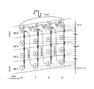
[Para 651 Part C: Balanced pulse pair white/white transition drive scheme
method of
the invention
[Para 66] As explained above, the balanced pulse pair white/white transition
drive scheme
(BPPWWTDS) of the present invention is intended to reduce or eliminate edge
artifacts when
driving bistable electro-optic displays. The BPPWWTDS requires the application
of one or
more balanced pulse pairs (a balanced pulse pair or "BPP" being a pair of
drive pulses of
opposing polarities such that the net impulse of the balanced pulse pair is
substantially zero)
during white-to-white transitions in pixels which can be identified as likely
to give rise to
edge artifacts, and are in a spatio-temporal configuration such that the
balanced pulse pair(s)
will be efficacious in erasing or reducing the edge artifact.
[Para 671 The BPPWWTDS attempts to reduce the visibility of accumulated errors
in a
manner which does not have a distracting appearance during the transition and
in a manner
that has bounded DC imbalance. This is effected by applying one or more
balanced pulse
pairs to a subset of pixels of the display, the proportion of pixels in the
subset being small
enough that the application of the balanced pulse pairs is not visually
distracting. The visual
distraction caused by the application of the BPP's may be reduced by selecting
the pixels to
which the BPP's are applied adjacent to other pixels undergoing readily
visible transitions.
For example, in one form of the BPPWWTDS, BPP's are applied to any pixel
undergoing a
white-to-white transition and which has at least one of its eight neighbors
undergoing a (not
white)-to-white transition. The (not white)-to-white transition is likely to
induce a visible
edge between the pixel to which it is applied and the adjacent pixel
undergoing the white-to-
white transition, and this visible edge can be reduced or eliminated by the
application of the
BPP's. This scheme for selecting the pixels to which BPP's are to be applied
has the
advantage of being simple, but other, especially more conservative, pixel
selection schemes
-19-
CA 02863425 2014-07-31
WO 2013/116494
PCT/US2013/024106
may be used. A conservative scheme (i.e., one which ensures that only a small
proportion of
pixels have BPP's applied during any one transition) is desirable because such
a scheme has
the least impact on the overall appearance of the transition.
[Para 681 As already indicated, the BPP's used in the BPPWWTDS of the present
invention
can comprise one or more balanced pulse pairs. Each half of a balanced pulse
pair may
consist of single or multiple drive pulses, provided only that each of the
pair has the same
amount. The voltages of the BPP's may vary provided only that the two halves
of a BPP must
have the same amplitude but opposite sign. Periods of zero voltage may occur
between the
two halves of a BPP or between successive BPP's. For example, in one
experiment, the
results of which are described below, the balanced BPP's comprises a series of
six pulses,
+15V, -15V, +15V, -15V, +15V, -15Võ with each pulse lasting 11.8 milliseconds.
It has been
found empirically that the longer the train of BPP's, the greater the edge
erasing which is
obtained. When the BPP's are applied to pixels adjacent to pixels undergoing
(non-white)-to-
white transitions, it has also been found that shifting the BPP's in time
relative to the (non-
white)-to-white waveform also affects the degree of edge reduction obtained.
There is at
present no complete theoretical explanation for these findings.
[Para 69] It was found in the experiment referred to in the preceding
paragraph that the
BPPWWTDS was effective in reducing the visibility of accumulated edges as
compared with
the prior art Global Limited (GL) drive scheme. Figure 6 of the accompanying
drawings
shows the differences in L* values of the various gray levels for the two
drive schemes, and it
will be seen that the L* differences for the BPPWWTDS are much closer to zero
(the ideal)
than those for the GL drive scheme. Microscopic examination of edge regions
after
applications of the BPPWWTDS shows two types of responses that can account for
the
improvement. In some cases it appears that the actual edge is eroded by the
application of the
BPPWWTDS. In other cases it appears that the edge is not much eroded, but
adjacent to the
dark edge another light edge is formed. This edge pair cancels out when viewed
from a
normal user distance.
[Para 70] In some cases, it has been found that application of the BPPWWTDS
can actually
over-correct for the edge effects (indicated in plots such as those of Figure
6 by the L*
differences assuming negative values). See Figure 7 which shows such over-
correction in an
experiment using a train of four BPP's. If such over-correction occurs, it has
been found that
it may reduced or eliminated by reducing the number of BPP's employed or by
adjusting the
temporal position of the BPP's relative to the (non-white)-to-white
transitions. For example,
-20-
CA 02863425 2014-07-31
WO 2013/116494
PCT/US2013/024106
Figure 8 shows the results of an experiment using from one to four BPP's to
correct edge
effects. With the particular medium being tested, it appears that two BPP's
give the best edge
correction. The number of BPP's and/or the temporal position of the BPP's
relative to the
(non-white)-to-white transitions could be adjusted in a time-varying manner
(i.e., on the fly)
to provide optimum correction of predicted edge visibility.
[Para 71] As already discussed, the drive schemes used for bistable electro-
optic media
should normally be DC balanced, i.e., the nominal DC imbalance of the drive
scheme should
be bounded. Although a BPP appears inherently DC balanced and thus should not
affect the
overall DC balance of a drive scheme, the abrupt reversal of voltage on the
pixel capacitor
which is normally present in backplanes used to drive bistable electro-optic
media (see, for
example, U. S. Patent No. 7,176,880) may result in incomplete charging of the
capacitor
during the second half of the BPP can in practice induce some DC imbalance. A
BPP applied
to a pixel none of whose neighbors are undergoing a non-zero transition can
lead to whitening
of the pixel or other variation in optical state, and a BPP applied to a pixel
having a
neighboring pixel undergoing a transition other than to white can result in
some darkening of
the pixel. Accordingly, considerable care should be exercised in choosing the
rules by which
pixels receiving BPP's are selected.
[Para 72] In one form of the BPPWWTDS of the present invention, logical
functions are
applied to the initial and final images (i.e., the images before and after the
transition) to
determine if a specific pixel should have one or more BPP's applied during the
transition. For
example, various forms of the BPPWWTDS might specify that a pixel undergoing a
white-to-
white transition would have BPP's applied if all four cardinal neighbors
(i.e., pixels which
share a common edge, not simply a corner, with the pixel in question) have a
final white
state, and at least one cardinal neighbor has an initial non-white state. If
this condition does
not apply, a null transition is applied to the pixel, i.e., the pixel is not
driven during the
transition. Other logical selection rules can of course be used.
[Para 73] Another variant of the BPPWWTDS in effect combines the BPPWWTDS with
the
SGU drive scheme of the present invention by applying a global complete drive
scheme to
certain selected pixels undergoing a white-to-white transition to further
increase edge
clearing. As noted above in the discussion of SGU drive schemes, the GC
waveform for a
white-to-white transition is typically very flashy so that it is important to
apply this waveform
only to a minor proportion of the pixels during any one transition. For
example, one might
apply a logical rule that the GC white-to-white waveform is only applied to a
pixel when
-21-
CA 02863425 2014-07-31
WO 2013/116494
PCT[US2013/024106
three of its cardinal neighbors are undergoing non-zero transitions during the
relevant
transition; in such a case, the flashiness of the GC waveform is hidden among
the activity of
the three transitioning cardinal neighbors. Furthermore, if the fourth
cardinal neighbor is
undergoing a zero transition, the GC white-to-white waveform being applied to
the relevant
pixel may edge an edge in the fourth cardinal neighbor, so that it may be
desirable to apply
BPP's to this fourth cardinal neighbor.
[Para 74] Other variants of the BPPWWTDS involve application of a GC white-to-
white
(hereinafter "GCWW" )transition to select areas of the background, i.e. areas
in which both
the initial and final states are white. This is done such that every pixel is
visited once over a
pre-determined number of updates, thereby clearing the display of edge and
drift artifacts
over time. The main difference from the variant discussed in the preceding
paragraph is that
the decision as to which pixels should receive the GC update is a based on
spatial position
and update number, not the activity of neighboring pixels.
[Para 75] In one such variant, a GCWW transition is applied to a dithered sub-
population of
background pixels on a rotating per-update basis. As discussed in Section A
above, this can
reduce the effects of image drift, since all background pixels are updated
after some pre-
determined number of updates, while only producing a mild flash, or dip, in
the background
white state during updates. However, the method may produce its own edge
artifacts around
the updated pixels which persist until the surrounding pixels are themselves
updated. In
accordance with the BPPWVVTDS, edge-reducing BPP's may be applied to the
neighbors of
the pixels undergoing a GCWW transition, so that background pixels can be
updated without
introducing significant edge artifacts.
[Para 76] In a further variant, the sub-populations of pixels being driven
with a GCWW
waveform are further segregated into sub-sub-populations. At least some of the
resultant sub-
sub-populations receive a time-delayed version of the GCWW waveform such that
only one
part of them is in the dark state at any given time during the transition.
This further
diminishes the impact of the already weakened flash during the update. Time
delayed
versions of the BPP signal are also applied to the neighbors of these sub-sub-
populations. By
this means, for a fixed reduction in exposure to image drift, the apparent
background flash
can be reduced. The number of sub-sub-populations is limited by the increase
in update time
(caused by the use of delayed sipals) that is deemed acceptable. Typically two
sub-sub-
populations would be used, which nominally increases the update time by one
fundamental
drive pulse width (typically about 240 ms at 25 C). Also, having overly sparse
sub-sub-
-22-
CA 02863425 2014-07-31
WO 2013/116494
PCT[US2013/024106
populations also makes the individual updating background pixels more obvious
psycho-
visually which adds a different type of distraction that may not be desirable.
[Para 77] Modification of a display controller (such as those described in the
aforementioned U. S. Patent No. 7,012,600) to implement the various forms of
the
BPPWWTDS of the present invention is straightforward. One or more buffers
stores gray
scale data representing the initial and final image for a transition. From
this data, and other
information such as temperature and drive scheme, the controller selects from
a lookup table
the correct waveform to apply to each pixel. To implement the BPPWWTDS, a
mechanism
must be provided to chose among several different transitions for the same
initial and final
gray states (in particular the states representing white), depending on the
transitions being
undergone by neighboring pixels, the sub-groups to which each pixel belongs,
and the
number of the update (when different sub-groups of pixels are being updated in
different
updates. For this purpose, the controller could store additional "quasi-
states" as if they were
additional gray levels. For example, if the display uses 16 gray tones
(numbered 0 to 15 in the
lookup table), states 16, 17, and 18 could be used to represent the type of
white transition that
is required. These quasi-state values could be generated at various different
levels in the
system, e.g. at the host level, at the point of rendering to the display
buffer, or at an even
lower level in the controller when generating the LUT address.
[Para 78] Several variants of the BPPWWTDS of the present invention can be
envisioned.
For example, any short DC balanced, or even DC imbalanced, sequence of drive
pulses could
be used in place of a balanced pulse pair. A balanced pulse pair could be
replaced by a top-off
pulse (see Section D below), or BPP's and top-off pulses can be used in
combination.
[Para 79] Although the BPPWWTDS of the present invention has been described
above
primarily in relation to white state edge reduction it may also be applicable
to dark state edge
reduction, which can readily be effected simply by reducing the polarity of
the drive pulses
used in the BPPWWTDS.
[Para 80] The BPPWWTDS of the present invention can provide a "flashless"
drive scheme
that does not require a periodic global complete update, which is considered
objectionable by
many users.
[Para 81] Part D: White/white top-off pulse drive scheme method of the
invention
[Para 82] As described above, a fourth method of the present invention for
reducing or
eliminating edge artifacts resembles the BPPWWTDS described above in that a
"special
pulse" is applied during white-to-white transitions in pixels which can be
identified as likely
-23-
CA 02863425 2014-07-31
WO 2013/116494
PCT[US2013/024106
to give rise to edge artifacts, and are in a spatio-temporal configuration
such that the special
pulse will be efficacious in erasing or reducing the edge artifact. However,
this fourth method
differs from the third in that the special pulse is not a balanced pulse pair,
but rather a "top-
off" or "refresh" pulse. The term "top-off' or "refresh" pulse is used herein
in the same
manner as in the aforementioned U. S. Patent No. 7,193,625 to refer to a pulse
applied to a
pixel at or near one extreme optical state (normally white or black) which
tends to drive the
pixel towards that extreme optical state. In the present case, the term "top-
off' or "refresh"
pulse refers to the application to a white or near-white pixel of a drive
pulse having a polarity
which drives the pixel towards its extreme white state. This fourth driving
method of the
present invention may hereinafter for convenience be referred to as the
"white/white top-off
pulse drive scheme" or "WWTOPDS" method of the invention.
[Para 83] The criteria for choosing the pixels to which a top-off pulse is
applied in the
WWTOPDS method of the present invention are similar to those for pixel choice
in the
BPPWWTDS method described above. Thus, the proportion of pixels to which a top-
off
pulse is applied during any one transition should be small enough that the
application of the
top-off pulse is not visually distracting. The visual distraction caused by
the application of the
top-off pulse may be reduced by selecting the pixels to which the top-off
pulse is applied
adjacent to other pixels undergoing readily visible transitions. For example,
in one form of
the WWTOPDS, a top-off pulse is applied to any pixel undergoing a white-to-
white transition
and which has at least one of its eight neighbors undergoing a (not white)-to-
white transition.
The (not white)-to-white transition is likely to induce a visible edge between
the pixel to
which it is applied and the adjacent pixel undergoing the white-to-white
transition, and this
visible edge can be reduced or eliminated by the application of the top-off
pulse. This scheme
for selecting the pixels to which top-off pulses are to be applied has the
advantage of being
simple, but other, especially more conservative, pixel selection schemes may
be used. A
conservative scheme (i.e., one which ensures that only a small proportion of
pixels have top-
off pulses applied during any one transition) is desirable because such a
scheme has the least
impact on the overall appearance of the transition. For example, it is
unlikely that a typical
black-to-white waveform would induce an edge in a neighboring pixel, so that
it is not
necessary to apply a top-off pulse to this neighboring pixel if there is no
other predicted edge
accumulation at the pixel. For example, consider two neighboring pixels
(designated P1 and
P2) that display the sequences:
P1: W->W->B->W->W and
-24-
CA 02863425 2014-07-31
WO 2013/116494
PCT[US2013/024106
P2: W->B->B->B->W.
While P2 is likely to induce an edge in P1 during its white-to-black
transition, this edge is
subsequently erased during the P1 black-to-white transition, so that the final
P2 black-to-
white transition should not trigger the application of a top-off pulse in P1.
Many more
complicated and conservative schemes can be developed. For example, the
inducement of
edges could be predicted on a per-neighbor basis. Furthermore, it may be
desirable to leave
some small number of edges untouched if they are below some predetermined
threshold.
Alternatively, it might not be necessary to clean up edges unless the pixel
will be in a state
where it is surrounded by only white pixels, since edge effects tend not to be
readily visible
when they lie adjacent an edge between two pixel having very different gray
levels.
[Para 84] It has been found empirically that, when application of a top-off
pulse to one pixel
is correlated with at least one of its eight neighbors undergoing a (not
white)-to-white
transition, the timing of the top-off pulse relative to the transition on the
adjacent pixel has a
substantial effect on the degree of edge reduction achieved, with the best
results being
obtained when the top-off pulse coincides with the end of the waveform applied
to the
adjacent pixel. The reasons for this empirical finding are not entirely
understood at present.
[Para 85] In one form of the WWTOPDS method of the present invention, the top-
off pulses
are applied in conjunction with an impulse banking drive scheme (as to which
see Section F
below). In such a combined WWTOPDS/IBDS, in addition to application of a top-
off pulse, a
clearing slideshow waveform (i.e., a waveform which repeatedly drives the
pixel to its
extreme optical states) is occasionally applied to the pixel when DC balance
is to be restored.
This type of drive scheme is illustrated in Figure 9 of the accompanying
drawings. Both top-
off and clearing (slideshow) waveforms are applied only when pixel selection
conditions are
met; in all other cases, the null transition is used. Such a slideshow
waveform will remove
edge artifacts from the pixel, but is a visible transition. The results of one
drive scheme of this
type are shown in Figure 10 of the accompanying drawings; these results may be
compared
with those in Figure 6, although it should be noted that the vertical scale in
different in the
two set of graphs. Due to the periodic application of the clearing pulse, the
sequence is not
monotonic. Since application of the slideshow waveform occurs only rarely, and
can be
controlled so that it only occurs adjacent other visible activity, so that it
is seldom noticeable.
The slideshow waveform has the advantage of essentially completely cleaning a
pixel, but
has the disadvantage of inducing in adjacent pixels edge artifacts that
require cleaning. These
adjacent pixels may be flagged as likely to contain edge artifacts and thus
requiring cleaning
-25-
CA 02863425 2014-07-31
WO 2013/116494
PCT[US2013/024106
at the next available opportunity, although it will be appreciated that the
resultant drive
scheme can lead to a complex development of edge artifacts.
[Para 86] In another form of the WWTOPDS method of the present invention, the
top-off
pulses the top-off pulses are applied without regard to DC imbalance. This
poses some risk of
long-term damage to the display, but possibly such a small DC imbalance spread
out over
long time frames should not be significant, and in fact due to unequal storage
capacitor
charging on the TFT in the positive and negative voltage directions commercial
displays
already experience DC imbalance of the same order of magnitude. The results of
one drive
scheme of this type are shown in Figure 11 of the accompanying drawings; these
results may
be compared with those in Figure 6, although it should be noted that the
vertical scale in
different in the two set of graphs.
[Para 87] The WWTOPDS method of the present invention may be applied such that
the
top-off pulses are statistically DC balanced without the DC imbalance being
mathematically
bounded. For example, "payback" transitions could be applied to balance out
"top-off"
transitions in a manner that would be balanced on average for typical electro-
optic media, but
no tally of net impulse would tracked for individual pixels. It is been found
that top-off pulses
that are applied in a spatio-temporal context which reduces edge visibility
are useful
regardless of the exact mechanism by which they operate; in some cases it
appears that edges
are significantly erased, while in other cases it appears the center of a
pixel is lightened to a
degree that it compensates locally for the darkness of the edge artifact.
[Para 88] Top-off pulses can comprise one or more than one drive pulse, and
may use a
single drive voltage or a series of differing voltages in different drive
pulses.
[Para 89] The WWTOPDS method of the present invention can provide a
"flashless" drive
scheme that does not require a periodic global complete update, which is
considered
objectionable by many users.
[Para 90] Part E: Straight edge extra pixels drive scheme method of the
invention
[Para 91] As already mentioned, the "straight edge extra pixels drive scheme"
or "SEEPDS"
method of the present invention seeks to reduce or eliminate edge artifacts
which occur along
a straight edge between driven and undriven pixels. The human eye is
especially sensitive to
linear edge artifacts, especially ones which extend along the rows or columns
of a display. In
the SEEPDS method, a number of pixels lying adjacent the straight edge between
the driven
and undriven areas arc in fact driven, such that any edge effects caused by
the transition do
not lie only along the straight edge, but include edges perpendicular to this
straight edge. It
-26-
CA 02863425 2014-07-31
WO 2013/116494
PCT[US2013/024106
has been found that driving a limited number of extra pixels in this manner
greatly reduces
the visibility of edge artifacts.
[Para 92] The basic principle of the SEEPDS method is illustrated in Figures
12A and 12B
of the accompanying drawings. Figure 12A illustrates a prior art method in
which a regional
or partial update is used to transition from a first image in which the upper
half is black and
the lower half white to a second image which is all white. Because a regional
or partial drive
scheme is used for the update, and only the black upper half of the first
image is rewritten, it
is highly likely that an edge artifact will result along the boundary between
the original black
and white areas. Such a lengthy horizontal edge artifact tends to be easily
visible to an
observer of the display and to be objectionable. In accordance with the SEEPDS
method, as
illustrated in Figure 12B, the update is split into two separate steps. The
first step of the
update turns certain white pixels on the notionally "undriven" side (i.e., the
side on which the
pixels are of the same color, namely white, in both the initial and final
images) of the original
blackiwhite boundary black; the white pixels thus driven black are disposed
within a series of
substantially triangular areas adjacent the original boundary, such that the
boundary between
the black and white areas becomes serpentine and that the originally straight
line border is
provided with numerous segments extending perpendicular to the original
boundary. The
second step turns all black pixels, including the "extra" pixels driven black
in the first step,
white. Even if this second step leaves edge artifacts along the boundary
between the white
and black areas existing after the first step, these edge artifacts will be
distributed along the
serpentine boundary shown in Figure 12B and will be far less visible to an
observer than
would similar artifacts extending along the straight boundary shown in Figure
12A. The edge
artifacts may, in some cases, be further reduced because some electro-optic
media display
less visible edge artifacts when they have only remained in one optical state
for a short period
of time, as have at least the majority of the black pixels adjacent the
serpentine boundary
established after the first step.
[Para 93] When choosing the pattern to be executed in the SEEPDS method, care
should be
taken to ensure that the frequency of the serpentine boundary shown in Figure
12B is not too
high. Too high a frequency, comparable to that of the pixel spacing, cause the
edges
perpendicular to the original boundary to have the appearance of being smeared
out and
darker, enhancing rather than reducing edge artifacts. In such a case, the
frequency of the
boundary should be reduced. However, too low a frequency can also render
artifacts highly
visible.
-27-
CA 02863425 2014-07-31
WO 2013/116494
PCT[US2013/024106
[Para 94] In the SEEPDS method, the update scheme may follow a pattern such
as:
-regional-> standard image [any amount of time] ¨region al (s I i ghtly
expanded
to capture the new edge)-> image with modified edge ¨regional-> next image
or:
-partial-> standard image [any amount of time] ¨partial-> image with
modified edge ¨partial-> next image
Alternatively, if full updates are being used in a specific region, the
pattern may be:
-full regional-> standard image [any amount of time] ¨regional(slightly
expanded to capture the new edge)-> next image
[Para 95] Provided there is no unacceptable interference with the electro-
optic properties of
the display, a display might make use of the SEEPDS method all the time,
according to the
following pattern:
-partial-> standard image w modified edge [any amount of time] ¨partial->
next image
[Para 96] In order to reduce edge artifacts over multiple updates, the SEEPDS
method could
be arranged to vary the locations of the curves of the serpentine boundary
such as that shown
in Figure 12B in order to reduce repeated edge growth on repeated updates.
[Para 97] The SEEPDS method can substantially reduce visible edge artifacts in
displays
that make use of regional and/or partial updates. The method does not require
changes in the
overall drive scheme used and some forms of the SEEMS method can be
implemented
without requiring changes to the display controller. The method can be
implemented via
either hardware or software.
[Para 98] Part F: Impulse bank drive scheme method of the invention
[Para 99] As already mentioned, in the impulse bank drive scheme (IBDS) method
of the
present invention, pixels are "allowed" to borrow or return impulse units from
a "bank" that
keeps track of impulse "debt". In general, a pixel will borrow impulse (either
positive or
negative) from the bank when it is needed to achieve some goal, and return
impulse when it is
possible to reach the next desired optical state using a smaller impulse than
that required for a
completely DC balanced drive scheme. In practice, the impulse-returning
waveforms could
include zero net-impulse tuning elements such as balanced pulse pairs and
period of zero
voltage to achieve the desired optical state with a reduced impulse.
[Para 10010bviously, and 1BDS method requires that the display maintain an
"impulse bank
register" containing one value for each pixel of the display. When it is
necessary for a pixel to
-28-
CA 02863425 2014-07-31
WO 2013/116494
PCT/US2013/024106
deviate from a normal DC balanced drive scheme, the impulse bank register for
the relevant
pixel is adjusted to denote the deviation. When the register value for any
pixel is non-zero
(i.e., when the pixel has departed from the normal DC balanced drive scheme)
at least one
subsequent transition of the pixel is conducted using a reduced impulse
waveform which
differs from the corresponding waveform of the normal DC balanced drive scheme
and which
reduces the absolute value of the register value. The maximum amount of
impulse which any
one pixel can borrow should be limited to a predetermined value, since
excessive DC
imbalance is likely to have adverse effects on the performance of the pixel.
Application-
specific methods should be developed to deal with situations where the
predetermined
impulse limit is reached.
[Para 101IA simple form of an IBDS method is shown in Figure 9 of the
accompanying
drawings. This method uses a commercial electrophoretic display controller
which is
designed to control a 16 gray level display. To implement the IBDS method, the
16 controller
states that are normally assigned to the 16 gray levels are reassigned to 4
gray levels and 4
levels of impulse debt. It will be appreciated that a commercial
implementation of an IBDS
controller would allow for additional storage to enable the full number of
gray levels to be
used with a number of levels of impulse debt; cf. Section G below. In the IBDS
method
illustrated in Figure 9, a single unit (-15V drive pulse) of impulse is
borrowed to perform a
top-off pulse during the white-to-white transition under predetermined
conditions (which
being a zero transition should normally have zero net impulse). The impulse is
repaid by
making a black-to-white transition which lacks one drive pulse towards white.
In the absence
of any corrective action, the omission of the one drive pulse tends to make
the resultant white
state slightly darker that a white state using the full number of drive
pulses. However, there
are several known "tuning" methods, such as a pre-pulse balanced pulse pair or
an
intermediate period of zero voltage, which can achieve a satisfactory white
state. If the
maximum impulse borrowing (3 units) is reached, a clearing transition is
applied that is 3
impulse units short of a full white-to-white slideshow transition; the
waveform used for this
transition must of course be tuned to remove the visual effects of the impulse
shortfall. Such a
clearing transition is undesirable because of its greater visibility and it is
therefore important
to design the rules for the IBDS to be conservative in impulse borrowing and
quick in
impulse pay back. Other forms of the IBDS method could make use of additional
transitions
for impulse payback thereby reducing the number of times a forced clearing
transition is
required. Still other forms of the IBDS method could make use of an impulse
bank in which
-29-
CA 02863425 2014-07-31
WO 2013/116494
PCT[US2013/024106
the impulse deficits or surpluses decay with time so that DC balance is only
maintained over
a short time scale; there is some empirical evidence that at least some types
of electro-optic
media only require such short term DC balance. Obviously , causing the impulse
deficits or
surpluses to decay with time reduces the number of occasions on which the
impulse limit is
reached and hence the number of occasions on which a clearing transition is
needed.
[Para 102]The IBDS method of the present invention can reduce or eliminate
several
practical problems in bistable displays, such as edge ghosting in non-flashy
drive schemes,
and provides subject-dependent adaption of drive schemes down to the
individual pixel level
while still maintaining a bound on DC imbalance.
[Para 103]Part G: Display controllers
[Para 104]As will readily be apparent from the foregoing description, many of
the methods
of the present invention require or render desirable modifications in prior
art display
controllers. For example, the form of GCMDS method described in Part B above
in which an
intermediate image is flashed on the display between two desired images (this
variant being
hereinafter referred to as the "intermediate image GCMDS" or "1I-GCMDS"
method) may
require that pixels undergoing the same overall transition (i.e., having the
same initial and
final gray levels) experience two or more differing waveforms depending upon
the gray level
of the pixel in the intermediate image. For example, in the II-GCMDS method
illustrated in
Figure 5, pixels which are white in both the initial and final images will
experience two
different waveforms depending upon whether they are white in the first
intermediate image
and black in the second intermediate image, or black in the first intermediate
image and white
in the second intermediate image, Accordingly, the display controller used to
control such a
method must normally map each pixel to one of the available transitions
according to the
image map associated with the transition image(s). Obviously, more than two
transitions may
be associated with the same initial and final states. For example, in the II-
GCMDS method
illustrated in Figure 4, pixels may be black in both intermediate images,
white in both
intermediate images, or black in one intermediate image and white in the
others, so that a
white-to-white transition between the initial and final images may be
associated with four
differing waveforms.
[Para 105]Various modifications of the display controller can be used to allow
for the storage
of transition information. For example, the image data table which normally
stores the gray
levels of each pixel in the final image may be modified to store one or more
additional bits
designating the class to which each pixel belongs. For example, an image data
table which
-30-
CA 02863425 2014-07-31
WO 2013/116494
PCT[US2013/024106
previously stored four bits for each pixel to indicate which of 16 gray levels
the pixel
assumes in the final image might be modified to store five bits for each
pixel, with the most
significant bit for each pixel defining which of two states (black or white)
the pixel assumes
in a monochrome intermediate image. Obviously, more than one additional bit
may need to
be stored for each pixel if the intermediate image is not monochrome, or if
more than one
intermediate image is used.
[Para 106]Alternatively, the different image transitions can be encoded into
different
waveform modes based upon a transition state map. For example, waveform Mode A
would
take a pixel through a transition that had a white state in the intermediate
image, while
waveform Mode B would take a pixel through a transition that had a black state
in the
intermediate image.
[Para 107]It is obvious desirable that both waveform modes begin updates
simultaneously,
so that the intermediate image appear smoothly, and for this purpose a change
to the structure
of the display controller will be necessary. The host processor (i.e., the
device which provides
the image to the display controller) must indicate to the display controller
that pixels loaded
into the image buffer arc associated with either waveform Mode A or B. This
capability does
not exist in prior art controllers. A reasonable approximation, however, is to
utilize the
regional update feature of current controllers (i.e., the feature which allows
the controller to
use different drive schemes in differing areas of the display) and to start
the two modes offset
by one scan frame. To allow the intermediate image to appear properly,
waveform Modes A
and B must be constructed with this single scan frame offset in mind.
Additionally the host
processor will be required to load two images into the image buffer and
command two
regional updates. Image 1 loaded into the image buffer must be a composite of
initial and
final images where only the pixels subject to waveform Mode A region are
changed. Once the
composite image is loaded the host must command the controller to begin a
regional update
using waveform Mode A. The next step is to load Image 2 into the image buffer
and
command a global update using waveform Mode B. Since pixels commanded with the
first
regional update command are already locked into an update, only the pixels in
the dark region
of the intermediate image assigned to waveform Mode B will see the global
update. With
today's controller architectures only a controller with a pipeline-per-pixel
architecture and/or
no restrictions on rectangular region sizes would be able to accomplish the
foregoing
procedure.
-31-
CA 02863425 2014-07-31
WO 2013/116494
PCT/1JS2013/024106
[Para 1081 Since each individual transition in waveform Mode A and waveform
Mode B is
the same, but simply delayed by the length of their respective first pulse,
the same outcome
may be achieved using a single waveform. Here the second update (global update
in previous
paragraph) is delayed by the length of the first waveform pulse. Then Image 2
is loaded into
the image buffer and commanded with a global update using the same waveform.
The same
freedom with rectangular regions is necessary.
[Para 109]Other modifications of the display controller are required by the
BPPWWTG
method of the invention described in Part C above. As already described, the
BPPWWTG
method requires the application of balanced pulse pairs to certain pixels
according to rules
which take account of the transitions being undergone by neighbors of the
pixel to which the
balanced pulse pairs may be applied. To accomplish this at least two
additional transitions are
necessary (transitions that are not between gray levels), however current four-
bit waveforms
cannot accommodate additional states, and therefore a new approach is needed.
Three options
are discussed below.
[Para 110]The first option is to store at least one additional bit for each
pixel, in the same
manner as described above with reference to a GCMDS method. For such a system
to work,
the calculation of the next state information must be made on every pixel
upstream of the
display controller itself. The host processor must evaluate initial and final
image states for
every pixel, plus those of its nearest neighbors to determine the proper
waveform for the
pixel. Algorithms for such a method have been proposed above.
[Para 1111The second option for implementing the BPPWWTG method is again
similar to
that for implementing the GCMDS method, namely encoding the additional pixel
states (over
and above the normal 16 states denoting gray levels) into two separate
waveform modes. An
example would be a waveform Mode A, which is a conventional 16-state waveform
that
encodes transitions between optical gray levels, and a waveform Mode B, which
is a new
waveform mode that encodes 2 states (state 16 and 17) and the transitions
between them and
state 15. However, this does raise the potential problem that the impulse
potential of the
special states in Mode B will not be the same as in Mode A. One solution would
be to have as
many modes as there arc white-to-white transitions and use only that
transition in each mode,
so producing Modes A, B and C, but this is very inefficient. Alternatively,
one could send
down a null waveform that maps the pixels making a Mode B to Mode A transition
to state 16
first, and then transitioning from state 16 in a subsequent Mode A transition.
-32-
CA 02863425 2014-07-31
WO 2013/116494
PCT[US2013/024106
[Para 112]In order to implement a dual mode waveform system such as this,
measures
similar to the Dual Waveform Implementation Option 3 can be considered.
Firstly, the
controller must determine how to alter the next state of every pixel through a
pixel-wise
examination of the initial and final image states of the pixel, plus those of
its nearest
neighbors. For pixels whose transition falls under waveform Mode A, the new
state of those
pixels must be loaded into the image buffer and a regional update for those
pixels must then
be commanded to use waveform Mode A. One frame later, the pixels whose
transition falls
under waveform Mode B, the new state of those pixels must be loaded into the
image buffer
and a regional update for those pixels must then be commanded to use waveform
Mode B.
With today's controller architectures only a controller with a pipeline-per-
pixel architecture
and/or no restrictions on rectangular region sizes would be able to accomplish
the foregoing
procedure.
[Para 113]A third option is to use a new controller architecture having
separate final and
initial image buffers (which are loaded alternately with successive images)
with an additional
memory space for optional state information. These feed a pipelined operator
that can
perform a variety of operations on every pixel while considering each pixel's
nearest
neighbors' initial, final and additional states, and the impact on the pixel
under consideration.
The operator calculates the waveform table index for each pixel and stores
this in a separate
memory location, and optionally alters the saved state information for the
pixel. Alternatively,
a memory format may be used whereby all of the memory buffers arc joined into
a single
large word for each pixel. This provides a reduction in the number of reads
from different
memory locations for every pixel. Additionally a 32-bit word is proposed with
a frame count
timestamp field to allow arbitrary entrance into the waveform lookup table for
any pixel (per-
pixel-pipelining). Finally a pipelined structure for the operator is proposed
in which three
image rows are loaded into fast access registers to allow efficient shifting
of data to the
operator structure.
[Para 114]The frame count timestamp and mode fields can be used to create a
unique
designator into a Mode's lookup table to provide the illusion of a per-pixel
pipeline. These
two fields allow each pixel to be assigned to one of 15 waveform modes
(allowing one mode
state to indicate no action on the selected pixel) and one of 8196 frames
(currently well
beyond the number of frames needed to update the display). The price of this
added
flexibility achieved by expanding the waveform index from 16-bits, as in prior
art controller
designs, to 32-bits, is display scan speed. In a 32-bit system twice as many
bits for every
-33-
CA 02863425 2014-07-31
WO 2013/116494
PCT/US2013/024106
pixel must be read from memory, and controllers have a limited memory
bandwidth (rate at
which data can be read from memory). This limits the rate at which a panel can
be scanned,
since the entire waveform table index (now comprised of 32-bit words for each
pixel) must
be read for each and every scan frame.
[Para 115]The operator may be a general purpose Arithmetic Logic Unit (ALU)
capable of
simple operations on the pixel under examination and its nearest neighbors,
such as:
Bitwise logic operations (AND, NOT, OR, XOR);
Integer arithmetic operations (addition, subtraction, and optionally
multiplication and division); and
Bit-shifting operations
[Para 116]Nearest neighbor pixels are identified in the dashed box surrounding
the pixel
under examination. The instructions for the ALU might be hard-coded or stored
in system
non-volatile memory and loaded into an ALU instruction cache upon startup.
This
architecture would allow tremendous flexibility in designing new waveforms and
algorithms
for image processing.
[Para 117]Consideration will now be given to the image pre-processing required
by the
various methods of the present invention. For a dual mode waveform, or a
waveform using
balanced pulse pairs, it may be necessary to map n-bit images to n+1-bit
states. Several
approaches to this operation may be used:
(a) Alpha
blending may allow dual transitions based upon a transition
map/mask. If a one-bit per pixel alpha mask is maintained that identifies the
regions associated with transition Mode A, and transition Mode B, this map
may be blended with the n-bit next image to create an n+1-bit transition
mapped image that can then use an n+1-bit waveform. A suitable algorithm is:
DP= ocIP+(1-a)M
{(if M=0, DP=0.5IP, Designating shift right 1-bit for IP data
if M=1, DP=IP, Designating no shift of data)}
Where DP = Display Pixel
IP = Image Pixel
M = Pixel Mask (either I or 0)
cc = 0.5
For the 5-bit example with 4-bit gray level image pixels discussed above, this
algorithm would place pixels located within the transition Mode A region
-34-
CA 02863425 2014-07-31
WO 2013/116494
PCT/US2013/024106
(designated by a 0 in the pixel Mask) into the 16-31 range, and pixels located
in the transition Mode B region into the 0-15 range.
(b) Simple raster operations may prove to be easier to implement. Simply
ORing the mask bit into the most significant bit of the image data would
accomplish the same ends.
(c) Additionally adding 16 to the image pixels associated with one of the
transition regions according to a transition map/mask would also solve the
problem.
[Para 118]For waveforms using balanced pulse pairs, the above steps may be
necessary but
are not sufficient. Where dual mode waveforms have a fixed mask, BPP's require
some non-
trivial computation to generate a unique mask necessary for a proper
transition. This
computation step may render a separate masking step needless, where image
analysis and
display pixel computation can subsume the masking step.
[Para 119]The SEEPDS method discussed in Part E above involves an additional
complication in controller architecture, namely the creation of "artificial"
edges, i.e., edges
which do not appear in the initial or final images but are required to define
intermediate
images occurring during the transition, such as that shown in Figure 12B.
Prior art controller
architecture only allows regional updates to be performed within a single
continuous
rectangular boundary, whereas the SEEPDS method (and possibly other driving
methods)
require a controller architecture that allows multiple discontinuous regions
of arbitrary shape
and size to be updated concurrently, as illustrated in Figure 13.
[Para 120]A memory and controller architecture which meets this requirement
reserves a
(region) bit in image buffer memory to designate any pixel for inclusion in a
region. The
region bit is used as a "gatekeeper" for modification of the update buffer and
assignment of a
lookup table number. The region bit may in fact comprise multiple bits which
can be used to
indicate separate, concurrently updateable, arbitrarily shaped regions that
can be assigned
different waveform modes, thus allowing arbitrary regions to be selected
without creation of
a new waveform mode.
-35-