Note: Descriptions are shown in the official language in which they were submitted.
CA 02863770 2014-08-05
WO 2013/117621 PCT/EP2013/052387
1
FLEXIBLE WAVEGUIDES FOR OPTICAL COHERENCE TOMOGRAPHY
BACKGROUND
Field
Embodiments described herein relate to the field of optical coherence
tomography.
Background
Optical coherence tomography (OCT) is an imaging technique employed to view
layers at different depths
of a sample. The layers can be combined to create a three-dimensional map of
the sample's surface and
depth up to a few millimeters. OCT imaging systems commonly collect
information of the sample's
structure on a line-by-line basis. Each line scan (also called an A-scan)
provides one-dimensional in-depth
information from a region of the sample. By scanning the light beam laterally
across the sample and then
grouping several A-scans, two- and three-dimensional models can be formed of
the sample. The
scanning is traditionally carried out by mechanical movement of an optical
element.
SUMMARY
Embodiments herein describe the use of a flexible substrate comprising a
plurality of waveguides to be
used with an OCT system.
In an embodiment, a system for depth-resolved imaging of a sample includes a
substrate of substantially
flexible material, a plurality of waveguides disposed on the substrate, an
optical element disposed at a
distal end of the plurality of waveguides, and one or more interferometers
configured to combine a
reference light with light received by at least a portion of the plurality of
waveguides to resolve
contributions from a given depth of the sample. The system further includes a
light guiding element
coupled between the plurality of waveguides and the one or more
interferometers.
In another embodiment, a system for depth-resolved imaging of a sample
includes a substrate of
substantially flexible material, a plurality of waveguides disposed on the
substrate, an optical element
disposed at a distal end of the plurality of waveguides, and one or more
interferometers configured to
combine a reference light with light received by at least a portion of the
plurality of waveguides to resolve
contributions from a plurality of depths of the sample. The system further
includes a light guiding element
coupled between the plurality of waveguides and the one or more
interferometers.
An example method of making an optical coherence tomography system includes
bonding a layer of
semiconducting material to a layer of flexible material. The layer of
semiconducting material is further
thinned to a thickness of less than 10 microns. The method includes patterning
the layer of
semiconducting material to form a plurality of waveguides bonded to the layer
of flexible material. The
method also includes bending the layer of flexible material having the
plurality of waveguides bonded
thereto and coupling the plurality of waveguides on the bent flexible material
to one or more
interferometers used to perform optical coherence tomography.
CA 02863770 2014-08-05
WO 2013/117621 PCT/EP2013/052387
2
Another example method of making an optical coherence tomography system
includes patterning a layer
of semiconducting material in a device layer of a SOI wafer to form a
plurality of waveguides and
depositing a first layer of flexible material over the plurality of waveguides
formed in the device layer. The
SOI wafer includes a layer structure having the device layer, a buried oxide
layer, and a handle layer.
The handle layer is etched to substantially remove the handle layer followed
by etching the buried oxide
layer to substantially remove the buried oxide layer. A second layer of
flexible material is deposited over
the plurality of waveguides such that the plurality of waveguides are
sandwiched between the first and
second layers of flexible material to form a flexible optical circuit. The
method further includes bending
the flexible optical circuit and coupling the plurality of waveguides on the
bent flexible optical circuit to one
or more interferometers used to perform optical coherence tomography.
BRIEF DESCRIPTION OF THE DRAWINGS/FIGURES
The accompanying drawings, which are incorporated herein and form a part of
the specification, illustrate
embodiments of the present invention and, together with the description,
further serve to explain the
principles of the invention and to enable a person skilled in the pertinent
art to make and use the
invention.
Figs. 1A-D illustrate a plurality of waveguides on a flexible substrate and
examples of bending the
substrate, according to embodiments.
Figs. 2A-D illustrate various views of the end of a catheter, according to
embodiments.
Fig. 3 illustrates a block diagram of an OCT system, according to an
embodiment.
Fig. 4 illustrates an example method, according to an embodiment.
Fig. 5 illustrates an example method, according to an embodiment.
DETAILED DESCRIPTION
Although specific configurations and arrangements are discussed, it should be
understood that this is
done for illustrative purposes only. A person skilled in the pertinent art
will recognize that other
configurations and arrangements can be used without departing from the spirit
and scope of the present
invention. It will be apparent to a person skilled in the pertinent art that
this invention can also be
employed in a variety of other applications.
It is noted that references in the specification to "one embodiment," "an
embodiment," "an example
embodiment," etc., indicate that the embodiment described may include a
particular feature, structure, or
characteristic, but every embodiment may not necessarily include the
particular feature, structure, or
characteristic. Moreover, such phrases do not necessarily refer to the same
embodiment. Further, when
a particular feature, structure or characteristic is described in connection
with an embodiment, it would be
within the knowledge of one skilled in the art to effect such feature,
structure or characteristic in
connection with other embodiments whether or not explicitly described.
CA 02863770 2014-08-05
WO 2013/117621 PCT/EP2013/052387
3
Overcoming the need for mechanical movement in an OCT scanner can be realized
by using a large
number of optical waveguides to collect light from multiple points on a
sample. Waveguides have
previously been fabricated in a planar lightwave circuit (PLC). The PLC may
further include active
elements to switch the path of the light between different waveguides or
modulate the frequency of the
light. However, waveguides fabricated in a PLC are, by definition, coplanar.
This hinders the use of a
PLC-based OCT system for applications which require radial or conical scanning
(such as endoscopy).
Furthermore, common endoscopic or catheter probes can be smaller than 3 mm
which limits the number
of useable waveguides along the edge of a PLC.
In an embodiment of the present invention, the waveguides are provided on a
flexible substrate. The
flexible substrate allows for the waveguides to be curled or bent into various
shapes and more efficiently
fill a given area. For example, the flexible substrate may be curled into a
tight spiral or layered in an
accordion-type shape. Once the flexible substrate has been manipulated into a
particular form, it may be
placed into a housing or any other type of packaging for protection and to
help the substrate maintain its
shape. For example, the flexible substrate may be curled and subsequently
placed into the cylindrical
housing of an endoscope to provide a dense array of waveguides within the
housing.
Fig. 1A illustrates an example of a flexible substrate 102 comprising a
plurality of waveguides 104. The
flexible substrate may be a polymer such as, for example and without
limitation, polydimethylsiloxane
(PDMS) or Parylene. The flexible substrate may also be a thin semiconductor
material. Flexible substrate
102 may be sufficiently flexible so as to roll or bend without tearing.
Flexible substrate 102 is configured to adapt to various shapes as may be
useful for different applications.
Once implemented onto flexible substrate 102, waveguides 104 can then be
arranged in a non-coplanar
fashion while still allowing for focusing optics to direct the light coming
out of the different waveguides 104
according to any desired sampling pattern.
Waveguides 104 may be made from a single polymer material, or may include a
combination of polymer
materials. For example, waveguides 104 may be made from any one of SU-8, PMMA,
PDMS, etc.
Waveguides 104 may also be made from a semiconductor material such as silicon,
or III-V semiconductor
materials such as gallium arsenide or indium phosphide. It should be
understood that impurities or other
material combinations may exist in the semiconductor materials, for example,
tertiary or quaternary
compounds.
Waveguides 104 may be fabricated on the surface of flexible substrate 102.
Surface patterning may
involve a variety of lithographic masking and etching techniques. Some
examples of etching techniques
include reactive ion etching, inductive coupled plasma etching, and wet
chemical etching. In another
embodiment, waveguides 104 may be formed via bulk micromachining in which the
material of
waveguides 104 is bonded to flexible substrate 102 and subsequently thinned to
a final thickness below
100 microns. Smaller single-mode or nearly single-mode waveguides may be
thinned to a final thickness
below 10 microns or below 1 micron. In one embodiment, the final thickness of
waveguides 104 is about 3
microns. Examples of thinning procedures include chemical mechanical
polishing, bulk wet etching, and
etching using a reactive gas such as xenon di-fluoride. Structural integrity
may be ensured through the
introduction of carrier layers with appropriate tensile strength yet
sufficient flexibility. Other wafer-level
CA 02863770 2014-08-05
WO 2013/117621 PCT/EP2013/052387
4
substrate transfer processes can be used to transfer waveguides formed as an
optical device layer onto
films such as substrate 102, as would be understood by one of skill in the
art.
In another example, waveguides 104 may be embedded within flexible substrate
102. Embedding
waveguides 104 may provide better optical mode containment within the
waveguide due to the same or
similar cladding material surrounding each waveguide. Substrate 102 may be
layered around waveguides
104 in order to embed waveguides 104. In another example, waveguides 104 may
be doped regions of a
semiconductor layer with a top semiconductor layer deposited over the doped
layer to embed waveguides
104. The semiconductor layers may be epitaxially grown or deposited using
chemical vapor deposition
techniques.
Waveguides 104 may be disposed on or within substrate 102 such that all of the
waveguides are parallel
to each other. When waveguides 104 are disposed onto a layer of a
semiconductor or plastic substrate,
they can create a flexible optical integrated circuit.
Figs. 1B-D illustrate various ways that one may bend substrate 102 into
different shapes. Fig. 1B shows
substrate 102, containing embedded waveguides 104, as rolled into a
cylindrical shape. Fig. 1C shows
substrate 102 rolled into itself to create a spiral pattern of waveguides 104.
Fig. 1D shows substrate 102
folded to create a layered pattern. The circular and the spiral arrangement of
substrate 102 are useful
when circular or conical scanning is required. Figs. 1C and 1D may be
particularly useful when dense
three-dimensional scanning patterns are desired. Other shapes may be
considered as well without
deviating from the scope or spirit of the invention.
Such a combination of waveguides and flexible substrate, when bent, can be
combined with active
elements to switch a light beam from one waveguide to another. In such a
manner, scanning may be
performed without the need for mechanical scanning means. The active elements
may be based on
electro-optic, thermo-optic, or carrier injection effects, for instance. In
combination with terminal optics
which focus the light coming out of each waveguide onto a different point of
the sample's surface, an
akinetic (without any moving parts) scanning system for OCT imaging can be
achieved.
Waveguides defined inside traditional PLCs are, by definition, coplanar. This
would hinder the use of an
akinetic PLC-based scanning system for some applications, such as endoscopic
or catheter-based OCT
systems, where special sample scanning schemes (e.g., radial scanning or
conical scanning) are needed.
Line scanners are generally inefficient for obtaining radial or conical image
information. The reason is that
the optical focusing system needed to convert the light beams from an array of
co-planar waveguides in a
PLC into a complex scanning pattern on the tissue is challenging to implement.
In order to solve this
problem, a system may use a flexible waveguide system such as the embodiments
described with respect
to Figs. 1A-1D.
Figs. 2A-D provide various views of the end of a catheter or endoscope which
includes a flexible
waveguide system, according to an embodiment. Elements shown in broken lines
are illustrated as being
within housing 201.
Fig. 2A illustrates a side view of a probe which includes a housing 201, a
light guiding element 202, a
flexible waveguide system 204, and an optical element 206 disposed at distal
end 208 of the probe. Light
guiding element 202 may be, for example, a single optical fiber or a bundle of
fibers. Alternatively, light
CA 02863770 2014-08-05
WO 2013/117621 PCT/EP2013/052387
guiding element 202 may be a planar waveguide fabricated on a substrate. In
one example, light guiding
element 202 is a waveguide fabricated on the same flexible substrate as
included in flexible waveguide
system 204.
Flexible waveguide system 204 may include a plurality of waveguides similar to
substrate 102 as
described in Figs. 1A-D. Additionally, flexible waveguide system 204 may be
rolled into a cylindrical or
spiral shape, for example. In an embodiment, a diameter of distal end 208 of
housing 201 is less than 3
mm. In another example, the diameter of distal end 208 is less than 1 mm.
Optical element 206 directs light coming out of flexible waveguide system 204
onto a sample, according to
an embodiment. Optical element 206 may be, for example, any number of lenses
and/or mirrors designed
to guide light exiting distal end 208 towards a sample to be imaged. Optical
element 206 may also be
designed to collect light scattered back off of the sample. In one embodiment,
optical element 206
includes at least one lens that is a gradient index (GRIN) lens. In another
example, optical element 206
includes one or more spherical lens components. Distal end 208 may
additionally or alternatively include
a mirror to direct the light at a specific angle as it exits from distal end
208. Such a mirror may also be
used for collecting light at a specific angle off of the sample. Such a mirror
may be a static mirror or a
moveable mirror.
Light guiding element 202 is configured to transmit light between flexible
waveguide system 204 and other
optical components not disposed within housing 201, according to an
embodiment. In another example,
other optical components are coupled directly with flexible waveguide system
204 within housing 201.
These other optical components may include electrical or thermal modulators to
change the frequency of
the light. Other optical components may also include one or more
interferometers to constructively and/or
destructively interfere the light. The interferometers may be utilized for
performing either time or
frequency domain optical coherence tomography.
Although only one light guiding element 202 is illustrated, it should be
understood that any number of light
guiding elements may be used to guide light from various waveguides within
flexible waveguide system
204 to other optical components of the system. Alternatively, one or more
optical switches may be utilized
to switch to a particular waveguide of the plurality of waveguides in flexible
waveguide system 204 to
couple light into light guiding element 202.
Fig. 2B illustrates a front view looking into distal end 208 of the probe,
according to an embodiment.
Optical element 206 may fill the region at distal end 208. As such, flexible
waveguide system 204 is
shown behind optical element 206 using broken lines. Flexible waveguide system
204 is wrapped in a
tube-like shape, according to an embodiment.
Fig. 2C illustrates a top view of the probe that includes flexible waveguide
system 204 and optical element
206 within housing 201, according to an embodiment. Light guiding element 202
can be seen connecting
to flexible waveguide system 204 within housing 201.
Fig. 2D illustrates a perspective view of the probe end. A cylindrical shape
of flexible waveguide system
204 disposed within the cylindrical housing 201 of the probe is observed,
according to an embodiment.
Light guiding element 202 may be coupled to a portion of flexible waveguide
system 204, according to an
embodiment, or it may be coupled to all waveguides in flexible waveguide
system 204. A single light
CA 02863770 2014-08-05
WO 2013/117621 PCT/EP2013/052387
6
guiding element 202 is illustrated; however, a plurality of light guiding
elements may be disposed around
substantially the entire circumference of flexible waveguide system 204 to
capture light from the
waveguides of flexible waveguide system 204.
Another optical element may be used to direct the light from light guiding
element 202 to one or more of
the waveguides on flexible waveguide system 204. For example, a multiplexer
may be disposed between
light guiding element 202 and flexible waveguide system 204. In another
example, the multiplexer is
disposed on the substrate of flexible waveguide system 204. The multiplexer
may include one or more of
optical switches, circulators, beam steering modulators, etc. The multiplexer
allows for the integration of
many optical paths via flexible waveguide system 204 with a single optical
path via light guiding element
202.
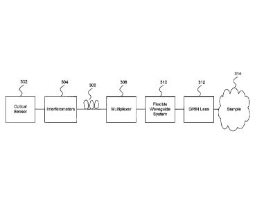
Fig. 3 illustrates a diagram of an example OCT system 300 which includes the
use of a flexible waveguide
system, according to an embodiment. OCT system 300 includes an optical sensor
302, one or more
interferometers 304, a light guiding element 306 which couples interferometers
304 to a multiplexer 308, a
flexible waveguide system 310, and an optical element 312. In the example
illustrated in Fig. 3, optical
element 312 is a GRIN lens. Not shown in Fig. 3 is a light source which would
produce light to be directed
onto a sample 314 at some distance from optical element 312. The light
produced from the light source
may also be directed down light guiding element 306 and through flexible
waveguide system 310 on its
way to sample 314. In an embodiment, the light source may also be used as a
reference light.
In one embodiment, one or more interferometers 304 are used to perform time
domain optical coherence
tomography (TD-OCT). The optical path length of a reference arm of the one or
more interferometers 304
is modulated so as to modulate a reference beam of light. When the modulated
reference beam is
combined with a beam of light received from sample 314, the resulting
interference resolves signal
contributions from a given depth of sample 314. The optical path length of the
reference arm may be
changed over time to yield image data at different depths of sample 314. The
modulation of the optical
path length is traditionally performed by mechanically moving one or more
mirrors in the path of the
reference light beam. However, other modulation techniques are to be
considered as well, such as, for
example, thermo-optic or electro-optic modulators coupled to a waveguide for
altering the optical path
length of the light within the waveguide.
In another embodiment, one or more interferometers 304 are used to perform
frequency domain optical
coherence tomography (FD-OCT). When performing FD-OCT, multiple depths of
sample 314 may be
analyzed substantially simultaneously by, for example, using a plurality of
spectrally separated detectors
at optical sensor 302. A Fourier transform may be performed on the signal
received by optical sensor 302
to resolve various signal components associated with various depths of sample
314. In one example,
performing FD-OCT allows for acquiring image information at various depths
without the need for
changing the optical path length of the reference arm in the one or more
interferometers 304.
Multiplexer 308 may be configured to transmit light through a first subset of
waveguides on flexible
waveguide system 310 while receiving light scattered back from sample 314 from
a second subset of
waveguides on flexible waveguide system 310. As light is reflected back from
sample 314 into optical
element 312, it travels back along light guiding element 306 to one or more
interferometers 304, according
CA 02863770 2014-08-05
WO 2013/117621 PCT/EP2013/052387
7
to one embodiment. In another example, the light may travel back to one or
more interferometers 304
using a different path than via light guiding element 306. One or more
interferometers 304 may combine
the light with a reference light to constructively and/or destructively
interfere the light. The resolved light
associated with either a given depth of sample 314 when performing TD-OCT, or
a plurality of depths of
sample 314 when performing FD-OCT, is collected at optical sensor 302.
Sample 314 may be a tissue sample, for example, a lining of a heart or a
colon. A plurality of locations on
sample 314 may be imaged at one time due to the plurality of waveguides
present in flexible waveguide
system 310. Additionally, radial and/or conical image information may be
collected from sample 314 due
to the circular arrangement of waveguides.
Fig. 4 illustrates a flowchart depicting a method 400 for fabricating an
optical coherence tomography
system, according to an embodiment of the invention. The fabrication of the
system may involve
fabricating a plurality of waveguides on a flexible material such as those
illustrated, for example, in Figs.
1B ¨ 1D. It is to be appreciated that method 400 may include operations
additional to those shown, or
perform the operations in a different order than shown.
Method 400 begins at step 402 where a semiconductor layer is bonded to a layer
of flexible material,
according to an embodiment. The semiconductor may be, for example, silicon or
gallium arsenide. The
flexible material may be, for example, PDMS or Parylene. The bonding may be
anodic, or may use other
techniques as would be known by one skilled in the relevant art(s) given the
description herein.
Method 400 continues with step 404 where the semiconductor layer is thinned.
The thinning may produce
a semiconductor layer having a thickness of less than 10 microns. In one
embodiment, the final thickness
of the semiconductor layer is around 3 microns. Chemical mechanical polishing
(CMP) may be utilized for
the thinning procedure. It should be understood that step 404 may not be
necessary in a case where the
semiconductor layer is already thin enough when initially bonded to the
flexible material.
In step 406, the semiconductor layer is patterned to form waveguides on the
flexible material, according to
an embodiment. The patterning of the semiconductor layer may involve
conventional lithography
techniques to first pattern a photoresist layer over the semiconductor layer
and subsequently etch the
exposed semiconductor material to form the waveguides. Alternatively, a hard
mask material such as
silicon nitride may be used in place of photoresist. In one embodiment, the
waveguides are formed as
substantially parallel lines on the flexible material. After the waveguides
are formed, a cladding material
may be deposited or added over the top of the waveguides to further confine
the light mode within the
waveg u id e core.
In step 408, the layer of flexible material having the plurality of waveguides
is bent into a particular shape,
according to an embodiment. In one example, the flexible material may be bent
into a cylindrical or spiral
shape as illustrated in Figs. 1B and 1C respectively. A generally circular
shape may aid the placement of
the flexible waveguides into a tubular-like apparatus such as a catheter or
endoscope. Other shapes may
be considered as well to more conveniently place the flexible waveguides into
various devices. The
various bent shapes of the waveguides can decrease the form factor of an
optical system and also
provide additional imaging techniques not readily available from strictly co-
planar waveguides.
CA 02863770 2014-08-05
WO 2013/117621 PCT/EP2013/052387
8
In step 410, the plurality of waveguides are coupled to one or more
interferometers, according to an
embodiment. The one or more interferometers combine the light received from at
least a portion of the
plurality of waveguides with a reference beam of light to perform OCT imaging.
The coupling between the
waveguides and the interferometers may involve any number of light guiding
elements, lenses, mirrors,
multiplexers etc. For example, a light guiding element, such as an optical
fiber, may be used to couple
light from the plurality of waveguides to the one or more interferometers. In
another example, one or
more lenses may be used to focus the light exiting from the plurality of
waveguides onto a light guiding
element, or directly onto an optical element integrated as part of the one or
more interferometers.
Fig. 5 illustrates a flowchart depicting a method 500 for fabricating an
optical coherence tomography
system, according to another embodiment of the invention. It is to be
appreciated that method 500 may
include operations additional to those shown, or perform the operations in a
different order than shown.
Method 500 begins at step 502 where a device layer of a Silicon-On-Insulator
(S01) wafer is patterned to
form waveguides, according to an embodiment. The SOI wafer may include a
semiconducting device
layer, a buried silicon dioxide layer, and a handle layer that may be up to
several hundred microns thick.
It should be appreciated, however, that the SOI wafer and fabrication process
described in method 500
should not be limited to using silicon as the device layer, and that other
semiconducting and polymer
materials could be used as well. As above, the patterning of the semiconductor
layer may involve
conventional lithography techniques to first pattern a photoresist layer over
the semiconductor layer and
subsequently etch the exposed semiconductor material to form the waveguides.
Alternatively, a hard
mask material such as silicon nitride may be used in place of photoresist. In
one embodiment, the
waveguides are formed as substantially parallel lines on the flexible
material. The device layer may have
a thickness of, for example, less than 10 microns. In one embodiment, the
final thickness of the device
layer is around 3 microns. After the waveguides are formed, a cladding
material may be deposited or
added over the top of the waveguides to further confine the light mode within
the waveguide core. Other
material layers or process steps could be added for additional electrical or
optical functionality.
Method 500 continues at step 504, where a thin layer of flexible material is
deposited on top of the SOI
wafer ensuring good adhesion to the device layer where the waveguides have
been defined, according to
an embodiment. The flexible material may be, for example, PDMS or Parylene.
Deposition will be done
through spinning, layer transfer based on temperature and pressure application
or other methods known
by one skilled in the relevant art(s) given the description herein. Adhesion
between the flexible material
and the device layer where the waveguides have been defined may be ensured
through surface
preparation using 02 plasma or other means, such as, for example, intermediate
adhesion promotion
layers. Other techniques for improving the adhesion may be used as would be
known by one skilled in
the relevant art(s) given the description herein.
Method 500 continues with step 506 where the SOI wafer with the flexible
material on top is attached to a
carrier substrate, according to an embodiment. Such attachment may be achieved
through a thin
adhesive layer, including a photoresist layer. The adhesive may be selected so
as to be easily removed
with a solvent without adversely affecting the flexible layer or the
waveguides. Such a solvent may be, for
example, acetone, methanol, isopropanol or any other organic or inorganic
solvent.
CA 02863770 2014-08-05
WO 2013/117621 PCT/EP2013/052387
9
Method 500 continues with step 508 where the handle layer of the SOI wafer is
etched, using the buried
oxide layer as a stop layer. This etching step can be done using wet
anisotropic etching, wet isotropic
etching, deep reactive ion etching, other plasma-based etching processes or
other means known by one
skilled in the relevant art(s) given the description herein. This etching step
can be modulated by a
lithography step, where solid silicon islands are protected through a soft or
hard mask. Such rigid islands
may be left on the buried oxide in as far as this may be needed to strengthen
the structure for packaging,
functional or other application needs.
In step 510, the buried oxide layer is subsequently etched away using an
etching solution, according to an
embodiment. In one example, the etching solution may be chosen to have either
a zero or negligible etch
rate for the waveguide material to protect the waveguides. Such an etchant may
be based on hydrofluoric
acid (HF), but other compositions are possible as would be known to one
skilled in the relevant art(s).
In step 512, another flexible layer is deposited on the exposed silicon
waveguides, according to an
embodiment. Step 512 is optional, however, the additional flexible layer
sandwiches the waveguides in
order to protect the optical circuit, add additional mechanical strength, and
improve the cladding around
the waveguides. In this step, further patterning of the flexible optical
circuit is possible, whereby arbitrary
shapes may be defined in the substrate. Such shapes may be used to enhance
flexibility, simplify
packaging, or other purposes. Patterning may be performed using lithography
masks to protect the
flexible optical circuit from the etching step. Etching of the flexible
optical circuit may be achieved, for
example, through plasma-based etching processes.
In step 514, the flexible optical circuit is released from the carrier
substrate, according to an embodiment.
The release may occur on the die level after cutting the flexible optical
circuit bonded to the carrier
substrate into dies of adequate size. The release may be performed by using a
solvent that dissolves the
adhesion layer only.
In step 516, the flexible optical circuit is bent into a particular shape,
according to an embodiment. In one
example, the flexible optical circuit may be bent into a cylindrical or spiral
shape as illustrated in Figs. 1B
and 1C respectively. A generally circular shape may aid the placement of the
flexible waveguides into a
tubular-like apparatus such as a catheter or endoscope. Other shapes may be
considered as well to
more conveniently place the flexible waveguides into various devices. The
various bent shapes of the
waveguides can decrease the form factor of an optical system and also provide
additional imaging
techniques not readily available from strictly co-planar waveguides.
In step 518, the plurality of waveguides on the flexible material are coupled
to one or more
interferometers, according to an embodiment. The one or more interferometers
combine the light
received from at least a portion of the plurality of waveguides with a
reference beam of light to perform
OCT imaging. The coupling between the waveguides and the interferometers may
involve any number of
light guiding elements, lenses, mirrors, multiplexers etc. For example, a
light guiding element, such as an
optical fiber, may be used to couple light from the plurality of waveguides to
the one or more
interferometers. In another example, one or more lenses may be used to focus
the light exiting from the
plurality of waveguides onto a light guiding element, or directly onto an
optical element integrated as part
of the one or more interferometers.
CA 02863770 2014-08-05
WO 2013/117621 PCT/EP2013/052387
Some embodiments of a flexible waveguide system described herein provide
certain structural
advantages. For example, waveguides disposed onto a flexible substrate may
have a size advantage
over standalone optical fibers, in that the waveguides disposed on a substrate
can be made much smaller
than a standalone fiber because the substrate can be used as structural
support for the waveguides.
Utilizing smaller waveguides allows for packing more waveguides over a given
area. As such, more
individual data points may be taken for a given surface area. Further, once
the waveguides have been
disposed on a substrate, the waveguides may be organized into a specific,
stable shape, which may not
be possible or easy with standalone optical fibers.
Embodiments of the present invention have been described above with the aid of
functional building
blocks illustrating the implementation of specified functions and
relationships thereof. The boundaries of
these functional building blocks have been arbitrarily defined herein for the
convenience of the
description. Alternate boundaries can be defined so long as the specified
functions and relationships
thereof are appropriately performed.
The foregoing description of the specific embodiments will so fully reveal the
general nature of the
invention that others can, by applying knowledge within the skill of the art,
readily modify and/or adapt for
various applications such specific embodiments, without undue experimentation,
without departing from
the general concept of the present invention. Therefore, such adaptations and
modifications are intended
to be within the meaning and range of equivalents of the disclosed
embodiments, based on the teaching
and guidance presented herein. It is to be understood that the phraseology or
terminology herein is for
the purpose of description and not of limitation, such that the terminology or
phraseology of the present
specification is to be interpreted by the skilled artisan in light of the
teachings and guidance.