Note: Descriptions are shown in the official language in which they were submitted.
CA 02863822 2014-08-06
WO 2013/117815 PCT/F12013/050129
A TOUCH SENSING DEVICE AND A DETECTION METHOD
FIELD OF THE INVENTION
The present invention relates to touch sensing
devices, more particularly to touch sensing devices
having touch sensitive films, and to a method of
detecting a touch and detecting its location.
BACKGROUND OF THE INVENTION
User interfaces for different kinds of electrical
apparatuses are nowadays more and more often made with
different types of touch sensing devices based on
touch sensitive films instead of conventional
mechanical buttons. Well known examples include
different kinds of touch pads and touch screens in
mobile phones, portable computers and similar devices.
In addition to the sophisticated and even luxurious
user experience achievable, touch sensing devices
based on touch sensitive films also provide a superior
freedom to the designers continuously trying to find
functionally more versatile, smaller, cheaper,
lighter, and also visually more attractive devices.
A key element in such touch sensing devices is a touch
sensitive film comprising one or more conductive
layers configured to serve as one or more sensing
electrodes. The general operating principle of this
kind of film is that the touch of a user by, e.g. a
fingertip or some particular pointer device is
detected by means of measuring circuitry to which the
touch sensitive film is connected. The actual
measuring principle can be e.g. resistive or
capacitive, the latter one being nowadays usually
considered the most advanced alternative providing the
best performance in the most demanding applications.
CA 02863822 2014-08-06
WO 2013/117815 PCT/F12013/050129
2
Capacitive touch sensing is based on the principle
that a touch on a touch sensitive film means, from
electrical point of view, coupling an external
capacitance to the measurement circuitry to which the
touch sensitive film is connected. With sufficiently
high sensitivity of the touch sensitive film, even no
direct contact on the touch sensitive film is
necessitated but a capacitive coupling can be achieved
by only bringing a suitable object to the proximity of
the touch sensitive film. The capacitive coupling is
detected in the signals of the measurement circuitry.
In a so called projected capacitive method, the
measurement circuitry includes drive electrodes and
sense electrodes used for supplying the signal and
sensing the capacitive coupling, respectively. This
circuitry is also arranged to rapidly scan over the
sensing electrodes sequentially so that coupling
between each supplying/measuring electrode pair is
measured.
Common for the known touch sensitive films in the
projected capacitive method is that the need to
properly determine the location of the touch
necessitates a high number of separate sensing
electrodes in the conductive layers. In other words,
the conductive layers are patterned into a network of
separate sensing electrodes. The more accurate
resolution is desired, the more complex sensing
electrode configuration is needed. One particularly
challenging issue is the detection of multiple
simultaneous touches which, on the other hand, often
is one of the most desired properties of the state-of-
the-art touch sensing devices. Complex sensing
electrode configurations and a high number of single
sensing electrode elements complicates the
manufacturing process as well as the measurement
electronics of the touch sensing device.
CA 02863822 2014-08-06
WO 2013/117815
PCT/F12013/050129
3
In touch screens, in addition to the touch sensing
capability, the touch sensitive film must be optically
transparent to enable use of the film in or on top of
a display of an electronic device, i.e. to enable the
display of the device to be seen through the touch
sensitive film. Moreover, transparency is also very
important from the touch sensitive film visibility
point of view. Visibility of the touch sensitive film
to the user of e.g. an LCD (Liquid Crystal Display),
an OLED (Organic Light Emitting Diode) display, or an
e-paper (electronic paper) display
seriously
deteriorates the user experience. So far, transparent
conductive oxides like ITO (Indium Tin Oxide) have
formed the most common group of the conductive layer
materials in touch sensitive films. However, from the
visibility point of view, they are far from an ideal
solution. The high refractive index of e.g. ITO makes
the patterned sensing electrodes visible. The problem
is emphasized as the sensing electrode patterning
becomes more complicated.
One promising new approach in touch sensitive films is
found in layers formed of or comprising networked
nanostructures. In addition to a suitable conductivity
performance, a layer consisting of networks of e.g.
carbon nanotubes (CNT), or carbon NANOBUDs having
fullerene or fullerene-like molecules covalently
bonded to the side of a tubular carbon molecule
(NANOBUDO is a registered trade mark of Canatu Oy),
can be made less visible to a human eye than e.g.
transparent conductive oxides like ITO, ATO or FTO.
Besides, as is well known, nanostructure-based layers
can possess flexibility, mechanical strength and
stability superior in comparison with e.g. transparent
conductive oxides.
CA 02863822 2014-08-06
WO 2013/117815
PCT/F12013/050129
4
One nanostructure-based solution is reported in US
2009/0085894 Al. According to the description thereof,
the nanostructures can be e.g. different types of
carbon nanotubes, graphene flakes, or nanowires.
Doping of the film is mentioned as a means for
increasing the electrical conductivity thereof. Two-
layer configurations based on mutual capacitance and
single-layer self-capacitance approaches are discussed
there. Multiple touch detection is stated to be
possible by means of the films disclosed. However, the
common problem of very complex electrode and
measurement circuitry configurations is not solved in
this document.
Another prior art solution is suggested in WO
2011/107666 Al. It discloses a touch sensing device
having a touch sensitive film, e.g. made of a network
of nanostructures, the film having sheet resistance
above 3.0 kg). While the problem of complex circuitry
is addressed in that invention, it still only suggests
operating with high resistance films and at limited
frequency ranges.
There is a need to provide a versatile touch sensing
device that has a simple sensing electrode
configuration, preferably enables single-
layer
capacitive operation principle, can operate at a wide
range of conductive film resistances, enables signal
frequency tuning for better noise control, and allows
using a wide variety of sensing algorithms.
PURPOSE OF THE INVENTION
The purpose of the present invention is to provide
novel solutions that have at least some or all the
above-mentioned advantages.
CA 02863822 2014-08-06
WO 2013/117815
PCT/F12013/050129
SUMMARY OF THE INVENTION
According to a first aspect of the invention there is
provided a touch sensing device, comprising: a touch
5 sensitive film comprising conductive material having a
resistance, the film being capable of capacitive or
inductive coupling to an external object when a touch
is made by said external object; a signal filter
formed at least by the resistance of the touch
sensitive film and the capacitive or inductive
coupling to the external object, the signal filter
having properties that are affected at least by the
location of the touch, the capacitance or inductance
of the touch or by a combination of said properties of
the touch; electrical circuitry resistively or
wirelessly coupled to the touch sensitive film at one
or more locations, the electrical circuitry being
configured to supply one or more excitation signals
having at least one frequency into the signal filter
and to receive one or more response signals from the
signal filter; and a processing unit resistively or
wirelessly coupled to the electrical circuitry,
wherein the processing unit is configured to detect
the presence or proximity of a touch by the external
object, the location of said touch, the capacitance or
inductance of said touch, or a combination thereof by
processing one or more response signals and thereby
measuring changes in the properties of the signal
filter.
A touch sensitive film means, in general, a film which
can be used as a touch sensitive element in a touch
sensing device. A touch sensing device is to be
understood here broadly to cover all user interface
devices operated by touching the device by an external
object, as well as other types of devices for
CA 02863822 2014-08-06
WO 2013/117815
PCT/F12013/050129
6
detecting the presence, proximity and location of such
objects.
The touch sensitive film of the present invention is
capable of capacitive or inductive coupling to an
external object, which means that a touch by an
external object causes changes in the filtering
properties of the film.
The word "touch" and derivatives thereof are used in
the context of the present invention in a broad sense
covering not only a direct mechanical or physical
contact between the fingertip, stylus, or some other
pointer or object and the touch sensitive film, but
also situations where such an object is in the
proximity of the touch sensitive film so that the
object generates sufficient capacitive or inductive
coupling between the touch sensitive film and the
ambient, or between different points of the touch
sensitive film. In this sense, the touch sensitive
film of the present invention can also be used as a
proximity sensor.
By "conductive material" is meant here any material
capable of allowing flow of electric charge in the
material, irrespective of the conductivity mechanism
or conductivity type of the material. Thus, conductive
material covers here, for instance, also
semiconductive or semiconducting materials. There can
be one or more layers of conductive material in a
touch sensitive film.
In addition to the conductive material, the touch
sensing device can also comprise other layers of
material and structures needed to implement an entire
working touch sensitive element. For example, there
can be one or more layers for mechanical protection of
CA 02863822 2014-08-06
WO 2013/117815
PCT/F12013/050129
7
the film. Moreover, there can be also one or more
layers for refractive index or color matching, and/or
one or more coatings, for instance, for anti-scratch,
decorative, water repellant, self-cleaning, or other
purposes. Besides the layered elements, the touch
sensitive film can also comprise three-dimensionally
organized structures, e.g. contact structures
extending through the touch sensitive film or a
portion thereof.
A signal filter is formed at least by the touch
sensitive film resistance and the capacitive or
inductive coupling to an external object. This signal
filter can be e.g. a low-pass filter, a high-pass
filter, a band-stop or band-pass filter. An example of
a low-pass filter would be an RC (resistor-capacitor)
series circuit across the input, with the output taken
across the capacitor. In an exemplary embodiment of
the present invention, the film resistance could
represent R and the capacitive coupling created by the
touch could represent C in the above low-pass filter.
By an "external object" is meant any capacitor or
inductor or capacitive or inductive pointer, e.g. a
human finger or a metal stylus, pointers having a
capacitive element or a metallic coil for inductive
coupling etc. For example, a stylus with a coil can be
either passive (no current is actively applied to the
coil) or active (an AC or DC current is applied to the
coil). A stylus with an active coil is generally used
to improve the accuracy, response time, or
transparency of the touch.
Forming of a signal filter by the resistance of the
touch sensitive film and the coupling to the external
object is based on an observation by the inventors
that such a filter changes its properties in response
CA 02863822 2014-08-06
WO 2013/117815 PCT/F12013/050129
8
to a touch from an external object, and that this
change can be measured to detect the touch, its
location and determine the capacitance or inductance
of the touch with a very high precision.
The electrical circuitry according to this embodiment
is resistively or wirelessly coupled to the touch
sensitive film at one or more locations. The circuitry
can comprise different types of contact electrodes,
wirings and other forms of conductors, switches, and
other elements needed to connect the touch sensitive
film and the one or more conductive layers thereof to
the rest of the touch sensing device. Resistive
connection implies physical contact, while e.g. radio
wave, inductive or capacitive coupling relates to
wireless coupling. Examples of resistive coupling
include but are not limited to soldering, clamps or
other traditional techniques.
The electrical circuitry is configured to supply one
or more excitation signals to the signal filter, and
to receive one or more response signals from the
filter. The electrical circuitry is connected to a
processing unit, as described below. In an exemplary
embodiment of the invention, the signals are sent to
the filter and received from it by the processing unit
via the electrical circuitry. The supplied one or more
excitation signals have at least one frequency,
amplitude and wave form. This means that each signal
may vary in frequency, amplitude or wave form or have
a constant frequency, amplitude and wave form, and, in
case of multiple signals, they may have equal or
different frequencies, amplitudes and wave forms. In
practice, electrical circuitry together with the
processing unit may be partly or fully integrated to a
single chip.
CA 02863822 2014-08-06
WO 2013/117815 PCT/F12013/050129
9
An excitation signal can be any electrical signal,
e.g. a pulsed, rise and fall time limited or
oscillating voltage or current, supplied to the signal
filter of the touch sensitive film via the circuitry
and providing conditions suitable for monitoring the
changes a touch induces in the filter properties. The
excitation signal could also be called, for example, a
drive signal or a stimulation signal. Typical examples
are AC current and/or voltage. A response signal is
correspondingly any measured electrical signal
received from the signal filter by using the circuitry
and allowing detection of a touch on the basis of
changes the touch causes to the filter properties and
detectable by this signal.
In an embodiment, the processing unit is resistively
or wirelessly coupled to the electrical circuitry. The
processing unit is configured to detect the presence
or proximity of a touch by the external object, the
location of said touch, the capacitance or inductance
of said touch, or a combination thereof by processing
one or more response signals and thereby measuring
changes in the properties of the signal filter.
The processing unit can comprise a processor, a signal
or pulse generator, a signal comparer, an
interpretation unit, and other hardware and
electronics as well as software tools necessary to
process the response signals.
The touch sensing device is capable of operation in a
single-layer mode utilizing a touch sensitive film
having one single conductive layer only. This is an
advantageous simplification in comparison with most
prior art capacitive touch sensitive films utilizing a
two-layer approach using different conductive layers
for the excitation and the response signals.
CA 02863822 2014-08-06
WO 2013/117815 PCT/F12013/050129
According to an embodiment, the electrical circuitry
is configured to receive one or more response signals
from the signal filter. In this embodiment, the
5 processing unit is configured to detect the presence
or proximity of a touch by the external object, the
location of said touch, the capacitance or inductance
of said touch, or a combination thereof, by comparing
said response signals to each other and thereby
10 measuring changes in the properties of the signal
filter. In an alternative embodiment, the processing
unit is configured to compare the response signals to
the excitation signals to measure changes in the
properties of the signal filter.
In an embodiment, an alternating current or voltage is
provided as an excitation signal to the signal filter
at one point thereof and alternating voltage or
current as a response signal is measured at another
point of the filter.
In an embodiment, the signal filter is further formed
by at least one external component. This at least one
external component is a part of the touch sensing
device of the above embodiments and it is resistively
or wirelessly coupled to the processing unit via the
electrical circuitry. The external component can be a
resistor, constant current source, capacitor or
inductor or a combination thereof. This external
component can be integrated into other units in the
device.
In an embodiment, an alternating current or voltage is
provided as an excitation signal to the signal filter
through an external component at one point thereof and
alternating voltage or current as a response signal is
measured at the same point of the filter.
CA 02863822 2014-08-06
WO 2013/117815
PCT/F12013/050129
11
According to an embodiment, the properties of the
signal filter are further affected by the distance
between said external object and the sensing film, the
capacitance or inductance of the external object,
physical properties of said external object, the
resistance of the film, the existence, thickness or
dielectric constant of a dielectric or insulating
layer between the sensitive film material and the
external object, or by a combination thereof.
The physical properties of the external object include
e.g. its geometry, material, orientation and
configuration.
According to an embodiment, the electrical circuitry
comprises one or more electrodes, and wherein at least
one of the electrodes is configured to supply said
excitation signal into the signal filter, and at least
one of the electrodes is configured to receive said
electrical response signal from the signal filter. The
number of the electrodes may vary depending on the
structure.
In one preferred embodiment, the measured properties
of the signal filter include amplitude response, phase
response, voltage response, current response or a
combination thereof. These properties can be affected
by the presence or proximity of a touch, its location
and its capacitance or inductance.
According to a preferred embodiment of the present
invention, the processing unit is further configured
to select one or more properties to be measured based
on at least one pre-determined frequency, amplitude
and wave form of the excitation signal so as to
maximize the signal to noise ratio and/or improve the
CA 02863822 2014-08-06
WO 2013/117815 PCT/F12013/050129
12
accuracy of the device at the pre-determined
frequency, amplitude and wave form.
An optimal excitation frequency depends on many
factors. Noise may increase at lower frequencies. On
the other hand, antenna effects disturbing the touch
detection becomes a problem at very high frequencies.
Antenna effects mean that different parts of the
measurement circuitry act like antennas tending to
couple disturbance signals between the circuitry and
the ambient. There usually is an optimal frequency
range between a lower and an upper cut-off frequency.
This range depends, for example, on the resistance of
the conductive material in the touch sensitive film,
the thickness and dielectric constant of any coating
layer over the film, the capacitance or inductance of
the external object, the frequencies of the
surrounding electronics and the material of the
substrate on which the conductive film lies. For
example, with a sufficient high frequency, a PET
substrate becomes conductive, thereby interfering with
the excitation and response signals. Therefore, the
ability to choose the operating frequency range, to
actively tune the frequency based on those factors
affecting the optimal frequency and to adjust the
device accordingly (i.e. by choosing the filter
property to be measured or the particular excitation
frequency within the operating range) is provided.
According to an embodiment, the touch sensitive film
of the touch sensing device extends as a continuous
structure in a plane. This means that the touch
sensitive film extends, for example, as solid, non-
interrupted, and non-patterned structure substantially
over the entire sensing area of the touch sensing
device, though, as in the case of, for instance, HARM
networks, the structure is not strictly continuous at
CA 02863822 2014-08-06
WO 2013/117815 PCT/F12013/050129
13
the nano or micro scale. This structure is also
optionally homogenous. This feature not only minimizes
the visibility of the conductive layer but also
simplifies the manufacturing thereof when no
patterning of the layer is needed. It also simplifies
the electronics of a touch sensing device having a
touch sensitive film according to this embodiment.
The good sensitivity and touch location resolution
performance of the touch sensitive film enable use of
such a non-patterned conductive layer in a single-
layer operation mode. Operation in a single-layer mode
means that only one single conductive layer is used in
touch sensing measurements. Multi-touch detection
capability is also available in a non-patterned
single-layer operation mode. Single-layer capability
as such also allows producing the entire touch
sensitive film as a rather thin structure.
In one embodiment, the touch sensitive film comprises:
a single stripe or two or more parallel stripes made
of the conductive material and extending over the
touch sensitive film in one direction and areas
between said stripes comprising non-conducting
material, wherein the electrical circuitry is
resistively or wirelessly coupled to each of the
stripes, and the processing unit is further configured
to detect the presence, proximity and location of the
touch along each stripe.
The electrodes of the electrical circuitry are coupled
to each stripe to supply and receive signals for
measurement. The touch location has to be determined
only in one dimension, and it is possible to use only
one electrode per stripe to do so.
CA 02863822 2014-08-06
WO 2013/117815 PCT/F12013/050129
14
In one embodiment, the touch sensitive film is formed
as a flexible structure so as to allow bending
thereof. A "flexible" structure means here a structure
allowing bending of the film, preferably repeatedly,
in at least one direction. In an embodiment, the touch
sensitive film is flexible in at least two directions
simultaneously.
Instead of or in addition to the flexibility, the
touch sensitive film can also be formed as a
deformable structure so as to allow deforming thereof,
e.g. by using thermoforming, along or over a three
dimensional surface.
Flexibility and/or deformability of the touch
sensitive film in combination with the measurement
features open entirely novel possibilities to
implement touch sensing devices. For example, a touch
sensitive film serving as the user interface of a
mobile device can be bent or formed to extend to the
device edges so that the touch sensitive film can
cover even the entire surface of the device. In a
touch sensitive film covering different surfaces of a
three-dimensional device, there can be several touch
sensing regions for different purposes. One sensing
region can cover the area of a display to form a touch
screen. Other sensing regions e.g. at the sides of the
device can be configured to serve as touch sensitive
element replacing the conventional mechanical buttons,
e.g. the power button or volume or brightness sliders
or dials.
A good choice for flexible and/or deformable touch
sensitive films is a conductive layer comprising one
or more HARMS (High Aspect Ratio Molecular Structure)
networks, as described in more detail below. HARM
structures and the networks thereof are inherently
CA 02863822 2014-08-06
WO 2013/117815
PCT/F12013/050129
flexible, thus enabling making the touch sensitive
film bendable and/or deformable.
Preferably, the touch sensitive film is optically
5 transparent, thus enabling use of the touch sensitive
film e.g. as part of a touch screen. Optical
transparency of the touch sensitive film means here
that at least 10 %, preferably at least 90 % of the
incident radiation from a direction substantially
10 perpendicular to the plane of the film, at the
frequency/wavelength range relevant in the application
at issue, is transmitted through the film. In most
touch sensing applications, this frequency/wavelength
range is that of visible light.
For the optical transparency, the key is the
conductive material of a touch sensitive film. The
requirement of simultaneous electrical conductivity
and optical transparency limits the number of possible
materials. In this sense, HARMS networks form a good
basis for an optically transparent touch sensitive
film because the HARMS networks can provide a
transparency superior to that of the transparent
conductive oxides, for example.
In one embodiment, the touch sensitive film comprises
a High Aspect Ratio Molecular Structure (HARMS)
network, a conductive polymer, graphene or a ceramic,
grids of metal such as silver or gold, or metal oxide.
By HARMS or HARM structures is meant here electrically
conductive structures with characteristic dimensions
in nanometer scale, i.e. dimensions less than or equal
to about 100 nanometers. Examples of these structures
include carbon nanotubes (CNTs), carbon NANOBUDs
(CNBs), metal nanowires, and carbon nanoribbons. In a
HARMS network a large number of these kinds of single
structures, e.g. CNTs, are interconnected with each
CA 02863822 2014-08-06
WO 2013/117815 PCT/F12013/050129
16
other. In other words, at a nanometer scale, the HARM-
structures do not form a truly continuous material,
such as, e.g., the conductive polymers or Transparent
Conductive Oxides, but rather a network of
electrically interconnected molecules. However, as
considered at a macroscopic scale, a HARMS network
forms a solid, monolithic material. HARMS networks can
be produced in the form of a thin layer.
The advantages achievable by means of the HARMS
network(s) in the sensitive film include excellent
mechanical durability and high optical transmittance
useful in applications requiring optically transparent
touch sensitive films, but also very flexibly
adjustable electrical properties. To maximize these
advantages, the conductive material can substantially
consist of one or more HARMS networks.
The resistivity performance of a HARMS network is
dependent on the density (thickness) of the layer and,
to some extent, also on the HARMS structural details
like the length, thickness, or crystal orientation of
the structures, the diameter of nanostructure bundles
etc. These properties can be manipulated by proper
selection of the HARMS manufacturing process and the
parameters thereof. Suitable processes to produce
conductive layers comprising carbon nanostructure
networks are described e.g. in WO 2005/085130 A2 and
WO 2007/101906 Al by Canatu Oy.
In one embodiment of the touch sensing device
according to the present invention, the touch sensing
device comprises also serves as a haptic interface
film. In other words, the device further comprises
means for providing a haptic feedback, preferably via
the sensitive film, in response to a touch. Providing
the haptic feedback via the sensitive film means that,
CA 02863822 2014-08-06
WO 2013/117815 PCT/F12013/050129
17
instead of the conventional approach based on separate
actuators attached to the touch sensitive film for
generating vibration of the touch sensitive film, the
sensitive film is used as a part of the means for
generating the haptic feedback. There are various
possibilities for this. A haptic effect can be
achieved by generating suitable electromagnetic
field(s) by means of the sensitive film. The skin of
the user touching the touch sensitive film senses
these fields as different sensations. This kind of
approach can be called capacitive haptic feedback
system. On the other hand, the sensitive film can
alternatively be used, for instance, as a part of an
electroactive polymer (artificial muscle) based haptic
interface, wherein the sensitive film forms one layer
of the interface.
One possibility to perform the both functions, i.e.
the touch detection and haptic feedback, is that the
sensitive film is alternately coupled to a touch
sensing circuitry and to means for producing the
signals for haptic feedback so that once a touch is
detected during a first time period, a haptic feedback
is then provided at a second time period following the
first one. The first and second time periods can be
adjusted to be so short that the user experiences the
device operating continuously.
One or more touch sensitive films can alternatively be
used, for instance, in conjunction with a fluidics
based haptic interface (as is under commercialization
by Tactus Technologies), wherein the touch sensitive
film is integrated with the flexible outer haptic film
which changes shape due to the pumping of a fluid into
flexible reservoirs. One or more touch sensitive films
can be on the inner and/or outer surfaces of the
flexible outer haptic film. In this case, the touch
CA 02863822 2014-08-06
WO 2013/117815 PCT/F12013/050129
18
sensitive film can be continuously coupled to the
touch sensing circuitry.
In one embodiment of the touch sensing device
according to the present invention, the touch sensing
film also serves as a deformation detecting film. This
means that the device incorporates means for e.g.
sensing bending, twisting and/or stretching of the
sensing film. This can be done by measuring changes in
the resistance between nodes or by changes in the
signal filter properties simultaneously with the touch
sensing according to the invention. As the signal
filtering properties of the system are a function of
the resistivity of the film and, at least for certain
materials, including but not limited to HARMs and
conductive polymers and in particular nanotubes and
NANOBUDs and more specifically, carbon nanotubes and
NANOBUDs, the signal filter properties can change if
the film is e.g. stretched, compressed or otherwise
deformed. By interpreting this change in either the
resistivity or signal filter properties, the present
invention can detect, for instance, elongation or
compression between nodes connected to the sensor
film. Thus, for example, sensing of elongation between
two sets of nodes at opposite corners indicates
bending, while sensing elongation in one direction and
compression in the other indicates twisting. In some
configurations, one or more nodes can be used to sense
in multiple directions. Alternative configurations are
possible according to the invention.
For certain deformable external objects, the
capacitance or inductance changes with the force
applied to the touch sensitive film and thus the
determined capacitance or inductance can be used as a
proxy for force. The force means e.g. a force which a
user applies to the device when performing a touch. A
CA 02863822 2014-08-06
WO 2013/117815 PCT/F12013/050129
19
human finger, for instance, deforms upon the
application of a force resulting in increased area in
proximity to the sensor film. This will cause the
capacitance to change accordingly. Alternatively, if
an inductive external object is used, and the user
deforms, for instance, a coil of the external object
or changes the distance from the coil to the surface
(e.g. via a spring), inductance changes accordingly
and force can be measured as well.
The touch sensing device of the present invention can
be implemented as a standard or customized stand-alone
module or as an non-separable unit integrated as a
part of some larger device, e.g. a mobile phone,
portable or tablet computer, e-reader, electronic
navigator, gaming console, refrigerator, blender,
dishwasher, washing machine, coffee machine, stove,
oven or other white goods surface, car dashboard or
steering wheel, etc.
According to one embodiment of the present invention,
the wireless coupling between parts of the device is
one of the following: coupling by radio waves,
coupling through magnetic fields, inductive or
capacitive coupling.
By "the wireless coupling between parts of the device"
is meant a wireless coupling between any device
elements described above.
The setup may require supplemental electronics that
handle the creation, sending and receiving of the data
and the AC current that creates either electrostatic
or electrodynamic induction between electrodes that
are located on both the main device and the touch
sensing module. These two devices may be wirelessly
CA 02863822 2014-08-06
WO 2013/117815
PCT/F12013/050129
coupled together by one or more of the following
methods:
- Electromagnetic induction (Inductive coupling,
electrodynamic induction), where the data and
5 power transmission is induced by current from a
magnetic field between opposing coils.
- Magnetic resonance is near field electromagnetic
inductive coupling through magnetic fields.
- Radio waves (e.g. RFID technology), wherein the
10 power is generated from the radio waves received
by the antenna, and the data transmission
substantially changes the radiated field load.
- Capacitive coupling (or electrostatic induction),
wherein the energy and data are transferred from
15 opposing planes of electrodes.
Touch sensors can be fully or partly integrated to the
application devices either by wires, directly soldered
or via connectors. This is sufficient in fixed
20 installations where the sensors typically are
positioned in areas that are not required to be open
apart. E.g. in portable devices they are typically
found in touch display applications, wherein the
display is actually beneath the touch sensing film and
the screen itself is permanently attached to the
device. If a touch sensing device is located on a
removable part of a device, then it would typically
require a connector by which it could connect to the
device once it is attached to it. This method is
functional but it may not be suitable in certain
applications. Moreover, even if a touch component is
intended to be permanently affixed to a device, there
are manufacturing costs and design limitations
associated with connecting the component via solder or
connectors.
CA 02863822 2014-08-06
WO 2013/117815 PCT/F12013/050129
21
In one embodiment of the present invention, a touch
sensing device is provided. It comprises a touch
sensing module comprising a touch sensitive film,
electrical circuitry configured to supply one or more
excitation signals to the touch sensing module and to
receive one or more response signals from the touch
sensitive module. In accordance with this embodiment,
the electrical circuitry is coupled to the touch
sensing module wirelessly.
In an embodiment, a 2- and 3-dimensional touch sensor
devices are provided to applications whose enclosure
cover has to be removed, for example to maintain and
change the serviceable parts inside. It is also a
robust method to provide data entry method to devices
requiring unbroken encapsulation for, for example,
wet, explosive or otherwise hazardous environments or
where direct connection, as with interconnecting
wires, is otherwise impossible, costly or highly
inconvenient.
In an embodiment, no physical connector for power and
data transmission that is susceptible to dirt, wear
and tear or breakage. With no connector there are
fewer parts susceptible to contamination, chemical or
physical degradation or mechanical damage thus
increasing the reliability of the device.
A direct physical contact can be avoided which, if not
secured firmly, may have an unintentional
disconnection and thus lead to data or power loss. It
may function as a remote control device to fixed
installations that takes the power from the
installation and works as an ad-hoc touch sensor or
generic data input output device.
CA 02863822 2014-08-06
WO 2013/117815
PCT/F12013/050129
22
By keeping the touch sensor functionalities in a
module and separating it from the main device, they
become different serviceable parts that can be
produced separately and combined together only at the
final assembly. An electrode can be implemented cost-
efficiently as a metal area or printed wire on printed
circuit board.
According to an embodiment, the touch sensor module
and the main device may be physically attached to each
other but the power or data or both are transmitted
wirelessly between them. In practice, the sensor,
excitation and sensing electronics together with the
data processing unit so that the whole unit is an
independent peripheral plug-in.
According to a second aspect of the present invention
there is provided a method for detecting the presence,
proximity, location, inductance, capacitance or a
combination of these features of an external object
with a touch sensing device, the method comprising:
supplying one or more electrical excitation signals
having at least one frequency, amplitude and wave form
into a signal filter formed at least by a resistance
of a touch sensitive film in the touch sensing device
and a capacitive or inductive coupling of said film
with the external object, receiving one or more
response signals from the signal filter, and detecting
the presence of a touch by the external object, or the
location of said touch by processing said one or more
response signals and thereby measuring changes in
properties of the signal filter.
Touch detection sensitivity and touch location
resolution of a touch sensing device do not depend on
the properties of signal filter and the processing
means performance only. Naturally it is also a matter
CA 02863822 2014-08-06
WO 2013/117815 PCT/F12013/050129
23
of, e.g., the contact electrode configuration. On the
other hand, the touch location resolution of the touch
sensitive film and a touch sensing device utilizing it
depend also on the number of the contact locations and
the placing of them with respect to each other and the
film. These are critical issues particularly in a
single-layer approach with a non-patterned conductive
layer. Typically, the earlier known devices of this
type, described e.g. in US 7,477,242 B2 and US
2008/0048996 Al, rely on a rectangular-shaped
conductive layer and four contact electrodes at the
corners thereof. However, this configuration
necessitates very complex signal processing, and the
accuracy of this device is quite low. It is
particularly hard to provide a flexible structure
according to that solution. Also, the multi-touch
capability can be very challenging to achieve with
that kind of approach. These difficulties are
mitigated or avoided in the present invention.
Below, the present invention is illustrated on the
basis of examples with references to the accompanying
drawings.
BRIEF DESCRIPTION OF THE DRAWINGS
Figures la, lb and lc illustrate one possible
configuration of a touch sensing device according to
the present invention.
Figures 2a, 2b and 2c illustrate another possible
configuration of a touch sensing device according to
the present invention.
Figures 3a and 3b are an illustration of a two-
dimensional unpatterned touch sensitive film according
to an embodiment.
Figures 4a, 4b and 4c show an embodiment having
deformation sensing capabilities.
CA 02863822 2014-08-06
WO 2013/117815 PCT/F12013/050129
24
Figure 5 illustrates another embodiment in which a
striped touch sensitive film is used.
Figure 6 shows an embodiment having U- and C-shaped
stripes in a grid.
Figures 7a and 7b are diagrams of compared received
response signals from a touch sensing device according
to the present invention.
Figures 8a, 8b and 8c are diagrams of received
response signals compared to excitation signals.
DETAILED DESCRIPTION OF THE INVENTION
An explanation of the invention follows based on the
examples described below.
Capacitive or inductive coupling to an external object
together with a resistive film compose an electronic
signal filter. A touch sensitive film with sufficient
electrical resistivity together with an external
object having capacitance or inductance creates a low-
pass RC filter due the resulting RC time constant of
the system. The properties of this low-pass filter
depend on the sheet resistance, as well as on location
and capacitance or inductance of the external object.
In the typical operational mode, one or more
oscillating signals or pulses are fed into the filter
at one or more locations. In the touch sensitive film,
the resistance between any two points on or at the
edge of the touch surface is a function of their
relative location and the geometry and sheet
resistance of the sensor area. The capacitance or
inductance in this system is a combination of
parasitic capacitance or inductance of the system and
the capacitance or inductance formed between the film
and coupled external object. A change in the
electronic filtering characteristics is substantial
CA 02863822 2014-08-06
WO 2013/117815 PCT/F12013/050129
when, in addition to the film's resistivity, there is
a load caused by one or more capacitively or
inductively coupled touches present in the system. By
measuring changes in the mentioned signal or pulse,
5 the change in the electronic filter characteristics
can be measured and thus the location of one or more
touches can be deduced. By measuring e.g. the change
in the current into the sensing film, the capacitance
or inductance between the sensor and the external
10 object can be calculated. Likewise, the signal changes
per sensing node (the part of the electrical
circuitry, connected to the touch sensitive film at a
particular location) indicate changes in relative
distance to the external object and, by comparing the
15 differences between the response signal at the sensing
nodes, together with knowledge of the total current
consumption and absolute values at the sensor nodes,
the relative position of the touch can be calculated
by various algorithms. For instance, the amplitudes of
20 the sampled pulses are in correlation to the touch
position and can be used for determining the actual
position.
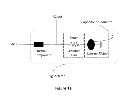
Figure la shows an embodiment wherein a signal is
25 supplied to a node and the effect of the low-pass
filter is measured via the same node. The system
consists of a touch sensitive film having a
resistivity and an external object that capacitively
or inductively couples to this touch sensing film. The
signal or pulse is introduced at a point in the
sensitive film, typically at an edge, though it may be
introduced anywhere in the film. An external component
such as a resistor, constant current source, capacitor
or inductor or combination thereof, can be used to,
for instance, increase the voltage linearity of the
measurement, distribute the current or potential more
evenly so as to avoid singularities in the system and
CA 02863822 2014-08-06
WO 2013/117815 PCT/F12013/050129
26
allow current or voltage potential to be measured. The
external component creates, together with the
resistive film and external touch object, a low-pass
filter. The signal couples to the load created by the
touch film and the external object and, by changing
the low-pass filter characteristics of the system,
thus altering the signal. The altered signal is
sampled (received) between the external component and
the touch sensitive film. For measuring multi-touch of
two or more external objects the measurement principle
is similar to single touch situation with the
distinction that instead of one there forms up to two
or more parallel paths to the external object
capacitance or inductance and the capacitive or
inductive coupling increases. The sampled signal is
different depending on the location and capacitance or
inductance of the external object and the interaction
of the signal with the low-pass filter formed by the
touch film, the external component and the external
object. Using multiple inputs / sensing nodes permits
one to more exactly specify the location of the touch
and the capacitance or inductance of the external
object. In the embodiment, to specify x and y
locations and the capacitance or inductance, 3 nodes,
that can be used in various possible combinations as
input and sensing nodes, are needed for each touch,
thus, e.g., for 4 simultaneous touches, 12 input and
sensing nodes are needed.
A more general configuration of the embodiment
according to Figure la is shown on a block diagram of
Figure lb, and a specific embodiment where three
signals or pulses are supplied via three external
components to three points (nodes) on the touch film
are illustrated on Figure lc. The sampled signals or
pulses are then compared to the source signal or pulse
or to other sampled signals or pulses to determine the
CA 02863822 2014-08-06
WO 2013/117815 PCT/F12013/050129
27
location and/or capacitance or inductance of the
external object.
Figure 2a shows an exemplary embodiment wherein a
signal is fed to a node and the effect of the low-pass
filter is measured in one or more opposing or adjacent
nodes. The system comprises a sensitive film having a
resistivity and an external object that capacitively
or inductively couples to this sensitive film. The
signal or pulse is introduced at a point in the
sensitive film, typically at an edge (though it may be
introduced anywhere) and the altered signal is
received at a different location. The received signal
is different depending on the location and capacitance
or inductance of the external object and the
interaction of the signal with the low-pass filter
formed by the touch film and the external object.
Using multiple sensing nodes for a single or multiple
input nodes permits more exact specification of the
location of the touch and the capacitance or
inductance of the external object. In the embodiment,
to specify x and y location and the capacitance or
inductance, 3 input and sensing nodes are needed for
each touch, thus, e.g., for 4 simultaneous touches, 12
input and sensing nodes are needed.
A more general configuration of the embodiment
according to Figure 2a is shown on a block diagram of
Figure 2b, and a specific embodiment where three
signals or pulses are supplied via three external
components to three points (nodes) on the touch film
are illustrated on Figure 2c. The sampled signals or
pulses are then compared to the source signal or pulse
or to other sampled signals or pulses to determine the
location and/or capacitance or inductance of the
external object.
CA 02863822 2014-08-06
WO 2013/117815
PCT/F12013/050129
28
In figures lb, lc, 2b and 2c the box "signal / pulse
generator" represents a generator that produces e.g.
one or more excitation voltage or current pulses or
oscillations (excitation signals) which can be, for
instance, sinusoidal, triangular, square or saw-
toothed in form. If needed, it may also include other
functionality such as a control unit and/or a clock.
The "signal comparer" box indicates a device that
compares and differentiates excitation and/or response
signals and provides this information to the
interpretation unit. It can compare, for instance,
voltage or current frequency, amplitude, phase shift,
or wave shape or form. The "interpretation unit" box
represents a unit that processes the signals out of
the signal comparer and possibly also uses information
from the signal / pulse generator (e.g. from the clock
or control functions). If needed, it may also include
other functionality such as a control unit and/or a
clock. It may also provide information to, for
instance, the signal / pulse generator (e.g. from the
clock or control functions). In practice, all these
functions may be incorporated in a single unit or chip
and thus may be not separate.
The excitation signals can be sent to individual nodes
and corresponding samples of the response signal can
be taken in sequence, or simultaneously. Furthermore,
the same or different excitation signals can be sent
to the individual nodes. The excitation signals can be
from the same or different sources.
Figure 3a is an illustration of an embodiment in which
a two dimensional touch sensitive film having multiple
input signals or pulses (which can be from a single or
multiple sources) is used. In this example, three
external components are each placed in series between
the source and an essentially two dimensional
CA 02863822 2014-08-06
WO 2013/117815 PCT/F12013/050129
29
sensitive film, or a sensitive sheet, and the signals
are sampled between the external components and the
sensitive film. In the case of no touch, the sampled
signals will have a given characteristic form in
relation to the properties of the filter. When a touch
occurs, the capacitive or inductive coupling to the
external object changes the filter characteristics.
The relationship between the sampled signals, either
to each other or to the input signal, provides
information on this change of characteristics and
therefore on location and capacitance or inductance of
the external object. In the embodiment, to specify x
and y location and the capacitance or inductance, 3
input and sensing nodes are needed for each touch,
thus, e.g., for 4 simultaneous touches, 12 input and
sensing nodes are needed. Thus, figure 3a shows the
minimum number of nodes to fully specify a single
touch in terms of location and capacitance or
inductance. Figure 3b shows another embodiment of the
same wherein four external components are each placed
in series between the source and an essentially two
dimensional sensitive film, or a sensitive sheet, and
the signals are sampled between the external
components and the sensitive film in order to increase
accuracy for a single touch or to, e.g., allow for the
determination of the presence of multiple touches. The
2-dimensional touch sensitive film described herein
may also be flexible and/or formable to a 3D surface.
Figures 4a-c show examples of sensing film deformation
with a single film, in which the sensitive film is
alternately coupled to a touch sensing circuitry or
algorithm and to a deformation sensing circuitry or
algorithm. In this case, at least three nodes are
required to perform the measurements. The deformation
can be determined by measuring changes in resistance
between nodes by a DC voltage level.
CA 02863822 2014-08-06
WO 2013/117815 PCT/F12013/050129
In practice, sensor deformation, twisting or bending
may impact the touch sensing by changing the active
region resistivity that again changes the filter
5 properties. However, in this case the touch sensitive
film can still be used at least in a mode wherein the
same film serves as a deformation sensor when it is
deformed, and as a touch sensor when no deformation is
made.
Figure 5 illustrates an embodiment of a two
dimensional touch sensor having multiple input signals
or pulses (which can be from a single or multiple
sources). An external component 51 is placed in series
between the source or sources, and either a single or
a set of essentially one dimensional sensing films (a
single or collection of sensing fingers or stripes 52)
and the signals are sampled between the external
components and the sensing films. The stripes should
have a high aspect ratio for good performance, e.g.
the length to width ratio should be greater than 3, or
more preferably, greater than 10. The stripes can be,
for instance, straight or curved and need not be of
constant width. In the case of a single stripe, the
embodiment may act as a slider or dial. In the case of
no touch the sampled signals will have a given
characteristic forms in relation to the properties of
the filter. When a touch occurs, the capacitive or
inductive coupling to the external object changes the
filter characteristics. The relationship between the
sampled signals to the input signal thus provides
information on the location of the external object and
the existence of a touch in any given strip. To also
detect the capacitance or inductance of the external
object, one or more additional samples can be taken
from the film, preferably at the opposite end of the
stripe 52. In the embodiment, to specify a touch
CA 02863822 2014-08-06
WO 2013/117815 PCT/F12013/050129
31
location along a stripe, e.g. the x location, and the
capacitance or inductance of a touch on said stripe, 2
input and sensing nodes are needed for each touch,
thus, e.g., for 4 simultaneous touches along any
stripe, 8 input and sensing nodes are needed. This can
be operated according to both configurations of figure
la and 2a. The location of a touch in the essentially
orthogonal, e.g. y, direction, is determined by
identifying the presence of a touch on a particular
stripe.
A modification of this configuration is to fabricate
each stripe as "U" or "C" shaped such that, in the
case of two electrodes per stripe, the electrodes are
located on the same side or edge of the touch region.
This can increase the accuracy of the device and
allows all the contact electrodes to be localized
along one edge, thus allowing design freedom and
reducing the need for, e.g. bezels one or more edges
of the touch area.
The configuration of figure 6 can be used also in a
two layer structure, each layer having a set of
stripes where the stripes of one layer are oriented so
as not to be parallel to the strips of the other
layer. Preferably, the orientation is at 90 degrees.
In this way a grid structure is formed. Figure 5 shows
this configuration in combination with "U" or "C"
shaped stripes. Typically the layers should be
separated by, e.g., an air gap or insulating or
dielectric material. A substrate or and coating can
serve as such an insulator or dielectric.
The markers "AC in" and "AC out" in figures 5 and 6
can mean a signal or pulse input and output,
respectively.
CA 02863822 2014-08-06
WO 2013/117815 PCT/F12013/050129
32
Figure 7a is a diagram showing a comparison of
response signals from a touch on a two-dimensional
rectangular touch surface having uniform resistivity
and six contact electrodes, two of which are at the
centerline edge and opposite each other. The figure
shows the difference between response signals between
these two contact node when a touch is initially
slightly offset to the left from the centerline, then
briefly on the centerline but slightly off center
toward the top, and then slightly off to right in the
end. The graphs show the signal differences between
different sensing nodes (receiving electrodes), i.e.
the measurements are performed according to the
embodiment of claim 4. In the ideal case the
difference is zero when the touch is at equal distance
and angle from the opposing sensing nodes as is the
case for the 2nd and 6th graphs. This clearly shows
how the changes in filter properties affect the signal
and how e.g. the touch location can be measured.
In Figure 7b the signals of Figure 7a are sampled at
fixed intervals as would be the case in real system.
Similarly, as opposed to a difference in response
signals at different nodes, the difference between the
response signal and the excitation signal can be used
to determine changes in the filter properties and thus
uniquely determine touch existence, proximity,
location and capacitance or inductance of the touch
object. Figures 8a-c show response signals compared to
excitation signals similarly to figures 7a and b. As
it is difficult to visually observe the difference in
the signals, figure 8c displays the response vs.
excitation signal difference when the touch is removed
at the time position 120 s.
CA 02863822 2014-08-06
WO 2013/117815 PCT/F12013/050129
33
Other properties of the response signal can also be
used to identify changes in the filter properties such
as the voltage or current wave form or shape, the
amplitude or the phase shift. The property or
properties to be sampled and used in the determination
of the changes in the filter property can be freely
chosen so that, e.g. the signal to noise ratio is
maximized. Moreover, the excitation signal frequency,
wave shape (e.g. sinusoidal, triangular, square, saw-
toothed etc.) and amplitude can be chosen to, for
instance, avoid interference or maximize signal to
noise ratio.
The invention is not limited to the examples described
above but the embodiments can freely vary within the
scope of the claims.