Note: Descriptions are shown in the official language in which they were submitted.
CA 02864202 2014-08-08
WO 2013/132250
PCT/GB2013/050550
COATED ELECTRICAL ASSEMBLY
Field of the Invention
The present invention relates to a coated electrical assembly and to methods
of preparing
a coated electrical assembly.
Back2round to the Invention
Conformal coatings have been used for many years in the electronics industry
to protect
electrical assemblies from environmental exposure during operation. A
conformal coating is a
thin, flexible layer of protective lacquer that conforms to the contours of an
electrical assembly,
such as a printed circuit board, and its components.
There are 5 main classes of conformal coatings, according to the IPC
definitions: AR
(acrylic), ER (epoxy), SR (silicones), UR (urethanes) and XY (paraxylylene).
Of these 5 types,
paraxylylene (or parylene) is generally accepted to offer the best chemical,
electrical and
physical protection. However, the deposition process is time consuming and
expensive, and the
starting material is expensive.
Parylene is polymer with the following structure:
n2
C _____________________________________________________
in
=
Parylene is deposited using a three stage vapour deposition process. A solid
precursor is heated
under vacuum and sublimes. It is important to appreciate that parylene,
although sometimes
erroneously called "paraxylene", is not in fact prepared from the compound
paraxylene. In fact,
the precursor is [2.2]paracyclophane:
1
CA 02864202 2014-08-08
WO 2013/132250
PCT/GB2013/050550
H2C
CH2
H2C
CH2
The chemical vapour is then passed through a high temperature furnace at
around 680 C, so that
the precursor splits into a reactive monomer. This reactive monomer then feeds
into a deposition
chamber and polymerizes on the surface of the substrate. Typical coating
thicknesses for
parylene are between 5 and 25 microns.
The parylene deposition technique described above is not ideal because of the
high cost
of the starting material, the high thermal energy consumption during monomer
generation, the
high vacuum requirements and the low growth rate.
There is therefore a need for conformal coatings that offer at least similar
levels of
chemical, electrical and physical protection as parylene, but that can be
manufactured more
easily and cheaply.
Summary of the Invention
The present inventors have surprisingly found that plasma polymerization of
relatively
inexpensive precursor compounds and deposition of the resulting polymers
results in a conformal
coating with excellent properties. The present invention thus relates to an
electrical assembly
which has a conformal coating, wherein said conformal coating is obtainable by
a method which
comprises plasma polymerization of a compound of formula (I) as defined below
and deposition
of the resulting polymer and plasma polymerization of a fluorohydrocarbon and
deposition of the
resulting polymer. The invention also relates to a method for conformally
coating an electrical
assembly, which method comprises plasma polymerization of a compound of
formula (I) as
defined below and deposition of the resulting polymer and plasma
polymerization of a
fluorohydrocarbon and deposition of the resulting polymer.
2
CA 02864202 2014-08-08
WO 2013/132250
PCT/GB2013/050550
The present invention thus relates to an electrical assembly which has a
conformal
coating, wherein said conformal coating is obtainable by a method which
comprises:
(a) plasma polymerization of a compound of formula (I) and deposition of the
resulting
polymer onto at least one surface of the electrical assembly:
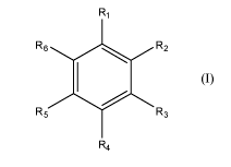
Ri
R6
R2
R5 R3
R4
(I)
wherein:
R1 represents Ci-C3 alkyl or C2-C3 alkenyl;
R2 represents hydrogen, Ci-C3 alkyl or C2-C3 alkenyl;
R3 represents hydrogen, C1-C3 alkyl or C2-C3 alkenyl;
R4 represents hydrogen, Ci-C3 alkyl or C2-C3 alkenyl;
R5 represents hydrogen, Ci-C3 alkyl or C2-C3 alkenyl; and
R6 represents hydrogen, Ci-C3 alkyl or C2-C3 alkenyl, and
(b) plasma polymerization of a fluorohydrocarbon and deposition of the
resulting
polymer onto the polymer formed in step (a).
The invention further relates to an electrical assembly which has a conformal
coating,
wherein said conformal coating is obtainable by a method which comprises:
(i) plasma polymerization of a fluorohydrocarbon and deposition of the
resulting polymer
onto at least one surface of the electrical assembly, and
(ii) plasma polymerization of a compound of formula (I) as defined above and
deposition
of the resulting polymer onto the polymer formed in step (i).
The invention also relates to a method for conformally coating an electrical
assembly,
which method comprises:
3
CA 02864202 2014-08-08
WO 2013/132250
PCT/GB2013/050550
(a) plasma polymerization of a compound of formula (I) as defined above and
deposition
of the resulting polymer onto at least one surface of the electrical assembly,
and
(b) plasma polymerization of a fluorohydrocarbon and deposition of the
resulting
polymer onto the polymer formed in step (a).
The invention further relates to a method for conformally coating an
electrical assembly,
which method comprises:
(i) plasma polymerization of a fluorohydrocarbon and deposition of the
resulting polymer
onto at least one surface of the electrical assembly, and
(ii) plasma polymerization of a compound of formula (I) as defined above and
deposition
of the resulting polymer onto the polymer formed in step (i).
The present inventors have surprisingly found that the coatings of the
invention provide
conformal coatings with excellent properties. In particular, it is finding of
the invention that a
multilayer coating comprising a layer of plasma polymerized fluorohydrocarbon
and a layer of
plasma polymerized compound of formula (I) provides a more effective conformal
coating than
would be expected for such a coating, based on the properties of single layer
coatings of the
polymers alone.
It is further finding of the invention been found that adding further layers
of the plasma
polymerized fluorohydrocarbon and/or the plasma polymerized compound of
formula (I), such
that the conformal coating comprises three or more layers, can provide further
improvements in
the properties of the conformal coating.
The improved performance of the conformal coating generally results in
improved
protection of the electrical assembly during operation.
A further advantage of the coatings of the invention is that the presence of
two discrete
polymer layers allows easy identification of the presence or absence of the
coating on a given
electrical assembly.
Description of the Fi2ures
Figure 1 shows an example of an electrical assembly of the invention which has
a
conformal coating.
4
CA 02864202 2014-08-08
WO 2013/132250
PCT/GB2013/050550
Figures 2 to 5 shows cross sections through the conformal coating in Figure 1,
and depict
the structure of preferred coatings.
Figure 6 shows the Fourier transform infrared (FTIR) spectrum for a
conventional
parylene conformal coating.
Figure 7 shows the FTIR spectrum for a conformal coating prepared in Example
1, by
plasma polymerization of 1,4-dimethylbenzene.
Figure 8 shows the FTIR spectrum for the multilayer conformal coatings
prepared in
Examples 2 to 4, which contain plasma polymerized 1,4-dimethylbenzene and
plasma
polymerized hexafluoropropylene.
Detailed Description of the Invention
The conformal coating of the invention is obtainable by plasma polymerization
of
specific precursor compounds and deposition of the resulting polymers. The
polymerization
reactions occur in situ. Polymerization therefore typically occurs on the
surface at which
deposition occurs. Polymerization and deposition are thus typically
simultaneous.
Plasma-polymerized polymers are a unique class of polymers which cannot be
prepared
by traditional polymerization methods. Plasma-polymerized polymers have a
highly disordered
structure and are generally highly crosslinked, contain random branching and
retain some
reactive sites. Plasma-polymerized polymers are thus chemically distinct from
polymers
prepared by traditional polymerization methods known to those skilled in the
art. These
chemical and physical distinctions are well known and are described, for
example in Plasma
Polymer Films, Hynek Biederman, Imperial College Press 2004.
Plasma polymerization is typically carried out in a reactor that generates a
gas plasma
which comprises ionized gaseous ions, electrons, atoms and/or neutral species.
A reactor
typically comprises a chamber, a vacuum system, and one or more energy
sources, although any
suitable type of reactor configured to generate a gas plasma may be used. The
energy source
may include any suitable device configured to convert one or more gases to a
gas plasma.
Preferably the energy source comprises a heater, radio frequency (RF)
generator, and/or
microwave generator.
5
CA 02864202 2014-08-08
WO 2013/132250
PCT/GB2013/050550
Typically, the electrical assembly is placed in the chamber of a reactor and a
vacuum
system is used to pump the chamber down to pressures in the range of 10-3 to
10 mbar. One or
more gases is typically then pumped into the chamber and an energy source
generates a stable
gas plasma. One or more precursor compounds is typically then be introduced,
as gases and/or
liquids, into the gas plasma in the chamber. When introduced into the gas
plasma, the precursor
compounds are typically ionized and/or decomposed to generate a range of
active species in the
plasma that polymerize to generate the polymer.
The exact nature and composition of the polymer deposited typically depends on
one or
more of the following conditions (i) the plasma gas selected; (ii) the
particular precursor
compound(s) used; (iii) the amount of precursor compound(s) (which may be
determined by the
combination of the pressure of precursor compound(s) and the flow rate); (iv)
the ratio of
precursor compound(s); (v) the sequence of precursor compound(s); (vi) the
plasma pressure;
(vii) the plasma drive frequency; (viii) the pulse width timing; (ix) the
coating time; (x) the
plasma power (including the peak and/or average plasma power); (xi) the
chamber electrode
arrangement; and/or (xii) the preparation of the incoming assembly.
Typically the plasma drive frequency is 1 kHz to 1 GHz. Typically the plasma
power is
100 to 250 W, preferably 150 to 200 W, for example about 175 W. Typically the
mass flow rate
is 5 to 100 sccm, preferably 5 to 20 sccm, for example about 10 sccm.
Typically the operating
pressure is 10 to 100 mTorr, for example about 50 mTorr. Typically the coating
time is 10
seconds to 20 minutes.
However, as a skilled person will appreciate, the preferred conditions will be
dependent
on the size and geometry of the plasma chamber. Thus, depending on the
specific plasma
chamber that is being used, it may be beneficial for the skilled person to
modify the operating
conditions.
It is preferable in the present invention to form the conformal coating by
depositing a first
polymer by plasma polymerization of a compound of formula (I), and then a
second polymer by
plasma polymerization of a fluorohydrocarbon. The resulting conformal coating
will thus
comprise two layers, which are preferably discrete. The first layer is in
contact with surface of
the electrical assembly and comprises the polymer formed by plasma
polymerization of the
6
CA 02864202 2014-08-08
WO 2013/132250
PCT/GB2013/050550
compound of formula (I). The second layer is in contact with the first layer
and comprises the
polymer formed by plasma polymerization of the fluorohydrocarbon.
Alternatively, the conformal coating can be formed by depositing a first
polymer by
plasma polymerization of a fluorohydrocarbon, and then a second polymer by
plasma
polymerization of a compound of formula (I). The resulting conformal coating
will thus
comprise two layers, which are preferably discrete. The first layer is in
contact with surface of
the electrical assembly and comprises the polymer formed by plasma
polymerization of the
fluorohydrocarbon. The second layer is in contact with the first layer and
comprises the polymer
formed by plasma polymerization of the compound of formula (I).
The deposition process of the invention can be repeated as often as desired,
to build up a
conformal coating comprising multiple layers, which are preferably discrete.
Where two or more
layers comprising a polymer formed by plasma polymerization of a compound of
formula (I) are
present, each compound of formula (I) used may be the same or different, and
are preferably the
same. Where two or more layers comprising a polymer formed by plasma
polymerization of a
fluorohydrocarbon are present, each fluorohydrocarbon used may be the same or
different, and
are preferably the same.
It is generally preferred that the polymer which is deposited last, that is to
say the
polymer that forms the upper or environmentally exposed surface of the
conformal coating, is
obtainable by plasma polymerization of a fluorohydrocarbon. However, the
polymer which is
deposited last, that is to say the polymer that forms the upper or
environmentally exposed surface
of the conformal coating, can also be obtainable by plasma polymerization of a
compound of
formula (I).
A particularly preferred conformal coating of the present invention comprises
four layers.
This conformal coating is obtainable by (a) plasma polymerization of a first
compound of
formula (I) and deposition of the resulting polymer onto at least one surface
of the electrical
assembly, then (b) plasma polymerization of a first fluorohydrocarbon and
deposition of the
resulting polymer onto the polymer formed in step (a), then (c) plasma
polymerization of a
second compound of formula (I) and deposition of the resulting polymer onto
the polymer
formed in step (b), and then (d) plasma polymerization of a second
fluorohydrocarbon and
deposition of the resulting polymer onto the polymer formed in step (c). The
compound of
7
CA 02864202 2014-08-08
WO 2013/132250
PCT/GB2013/050550
formula (I) and fluorohydrocarbon are preferably as defined below, and more
preferably are 1,4-
dimethylbenzene and hexafluoropropylene (C3F6).
A further particularly preferred conformal coating of the present invention
comprises six
layers. This conformal coating is obtainable by (a) plasma polymerization of a
first compound of
formula (I) and deposition of the resulting polymer onto at least one surface
of the electrical
assembly, then (b) plasma polymerization of a first fluorohydrocarbon and
deposition of the
resulting polymer onto the polymer formed in step (a), then (c) plasma
polymerization of a
second compound of formula (I) and deposition of the resulting polymer onto
the polymer
formed in step (b), then (d) plasma polymerization of a second
fluorohydrocarbon and deposition
of the resulting polymer onto the polymer formed in step (c), then (e) plasma
polymerization of a
third compound of formula (I) and deposition of the resulting polymer onto the
polymer formed
in step (d), and then (0 plasma polymerization of a third fluorohydrocarbon
and deposition of the
resulting polymer onto the polymer formed in step (e). The compound of formula
(I) and
fluorohydrocarbon are preferably as defined below, and more preferably are 1,4-
dimethylbenzene and hexafluoropropylene (C3F6).
A further particularly preferred conformal coating of the present invention
comprises
eight layers. This conformal coating is obtainable by (a) plasma
polymerization of a first
compound of formula (I) and deposition of the resulting polymer onto at least
one surface of the
electrical assembly, then (b) plasma polymerization of a first
fluorohydrocarbon and deposition
of the resulting polymer onto the polymer formed in step (a), then (c) plasma
polymerization of a
second compound of formula (I) and deposition of the resulting polymer onto
the polymer
formed in step (b), then (d) plasma polymerization of a second
fluorohydrocarbon and deposition
of the resulting polymer onto the polymer formed in step (c), then (e) plasma
polymerization of a
third compound of formula (I) and deposition of the resulting polymer onto the
polymer formed
in step (d), then (0 plasma polymerization of a third fluorohydrocarbon and
deposition of the
resulting polymer onto the polymer formed in step (e), then (g) plasma
polymerization of a
fourth compound of formula (I) and deposition of the resulting polymer onto
the polymer formed
in step (0, and then (h) plasma polymerization of a fourth fluorohydrocarbon
and deposition of
the resulting polymer onto the polymer formed in step (g). The compound of
formula (I) and
8
CA 02864202 2014-08-08
WO 2013/132250
PCT/GB2013/050550
fluorohydrocarbon are preferably as defined below, and more preferably are 1,4-
dimethylbenzene and hexafluoropropylene (C3F6).
Another particularly preferred conformal coating of the present invention
comprises three
layers. This conformal coating is obtainable by (i) plasma polymerization of a
first
fluorohydrocarbon of formula (I) and deposition of the resulting polymer onto
at least one
surface of the electrical assembly, then (ii) plasma polymerization of a
compound of formula (I)
and deposition of the resulting polymer onto the polymer formed in step (i),
and then (iii) plasma
polymerization of a second fluorohydrocarbon and deposition of the resulting
polymer onto the
polymer formed in step (ii). The compound of formula (I) and fluorohydrocarbon
are preferably
as defined below, and more preferably are 1,4-dimethylbenzene and
hexafluoropropylene (C3F6).
Another particularly preferred conformal coating of the present invention
comprises five
layers. This conformal coating is obtainable by (i) plasma polymerization of a
first
fluorohydrocarbon of formula (I) and deposition of the resulting polymer onto
at least one
surface of the electrical assembly, then (ii) plasma polymerization of a first
compound of
formula (I) and deposition of the resulting polymer onto the polymer formed in
step (i), and then
(iii) plasma polymerization of a second fluorohydrocarbon and deposition of
the resulting
polymer onto the polymer formed in step (ii), then (iv) plasma polymerization
of a second
compound of formula (I) and deposition of the resulting polymer onto the
polymer formed in
step (iii), and then (v) plasma polymerization of a third fluorohydrocarbon
and deposition of the
resulting polymer onto the polymer formed in step (iv). The compound of
formula (I) and
fluorohydrocarbon are preferably as defined below, and more preferably are 1,4-
dimethylbenzene and hexafluoropropylene (C3F6).
The thickness of the conformal coating of the present invention will depend
upon the
number of layers of each polymer that are deposited. The or each layer
obtainable by plasma
polymerization of a compound of formula (I) typically has a mean-average
thickness of 250 to
350 nm, preferably 275 to 325 nm, for example about 300 nm. The or each layer
obtainable by
plasma polymerization of a fluorohydrocarbon typically has a mean-average
thickness of 25 to
100 nm, preferably 50 to 75 nm.
Thus, if the conformal coating of the invention has one layer obtainable by
plasma
polymerization of a compound of formula (I) and one layer obtainable by plasma
polymerization
9
CA 02864202 2014-08-08
WO 2013/132250
PCT/GB2013/050550
of a fluorohydrocarbon, then typically the mean-average thickness of the
conformal coating is
275 to 450 nm, preferably 325 to 400 nm.
Similarly, if the conformal coating of the invention has two layers obtainable
by plasma
polymerization of a compound of formula (I) and two layers obtainable by
plasma
polymerization of a fluorohydrocarbon, then typically the mean-average
thickness of the
conformal coating is 550 to 900 nm, preferably 650 to 800 nm.
The thickness of each layer can be easily controlled by a skilled person.
Plasma
polymerization deposits the polymer at a uniform rate, and thus the thickness
of a layer of
polymer deposited is proportional to the deposition time. Accordingly, once
the rate of
deposition has been determined, a layer with a specific thickness can be
deposited by controlling
the duration of deposition.
The thickness of the conformal coating may be substantially uniform or may
vary from
point to point.
Precursor compounds of formula (I) have the following structure:
Ri
R6
R2
R5 R3
R4
(I)
wherein Ri represents Ci-C3 alkyl or C2-C3 alkenyl; R2 represents hydrogen, Ci-
C3 alkyl
or C2-C3 alkenyl; R3 represents hydrogen, C1-C3 alkyl or C2-C3 alkenyl; R4
represents hydrogen,
C1-C3 alkyl or C2-C3 alkenyl; R5 represents hydrogen, C1-C3 alkyl or C2-C3
alkenyl; and
R6 represents hydrogen, C1-C3 alkyl or C2-C3 alkenyl.
As used herein, the term C1-C3 alkyl embraces a linear or branched hydrocarbon
radical
having 1 to 3, preferably 1 to 2 carbon atoms. Examples include methyl, ethyl,
n-propyl and i-
propyl.
CA 02864202 2014-08-08
WO 2013/132250
PCT/GB2013/050550
As used herein, the term C2-C3alkenyl embraces a linear or branched
hydrocarbon
radical having 2 or 3 carbon atoms and a carbon-carbon double bond. A
preferred example is
vinyl.
Typically, R1 represents methyl or vinyl. Typically, R2 represents hydrogen,
methyl or
vinyl. Typically, R3 represents hydrogen, methyl or vinyl. Typically, R4
represents hydrogen,
methyl or vinyl. Typically, R5 represents hydrogen, methyl or vinyl,
preferably hydrogen.
Typically, R6 represents hydrogen, methyl or vinyl, preferably hydrogen.
Preferably, R5 and R6 represent hydrogen.
More preferably, R1 represents methyl or vinyl, R2 represents hydrogen, methyl
or vinyl,
R3 represents hydrogen, methyl or vinyl, R4 represents hydrogen, methyl or
vinyl, R5 represents
hydrogen and R6 represents hydrogen.
It is generally preferred that two of R2 to R4 represent hydrogen.
Preferred compounds of formula (I) are 1,4-dimethylbenzene, 1,3-
dimethylbenzene, 1,2-
dimethylbenzene, toluene, 4-methyl styrene, 3-methyl styrene, 2-methyl
styrene, 1,4-divinyl
benzene, 1,3-divinyl benzene or 1,2-divinyl benzene. 1,4-dimethylbenzene is
particularly
preferred.
A fluorohydrocarbon is a hydrocarbon material comprising fluorine atoms.
Preferred
fluorohydrocarbons are perfluoroalkanes, perfluoroalkenes, perfluoroalkynes,
fluoroalkanes,
fluoroalkenes and fluoroalkynes, wherein said compounds preferably contain up
to 10 carbon
atoms, more preferably up to five carbon atoms. Preferred examples include
CF4, C2F4, C2F6,
C3F6, C3F8 and C4F8. A most preferred fluorohydrocarbon is hexafluoropropylene
(C3F6).
It is particularly preferred that the or each compound of formula (I) is 1,4-
dimethylbenzene, 1,3-dimethylbenzene, 1,2-dimethylbenzene, toluene, 4-methyl
styrene, 3-
methyl styrene, 2-methyl styrene, 1,4-divinyl benzene, 1,3-divinyl benzene or
1,2-divinyl
benzene, and the or each fluorohydrocarbon is CF4, C2F4, C2F6, C3F6, C3F8 or
C4F8. A
particularly preferred combination is 1,4-dimethylbenzene and
hexafluoropropylene (C3F6).
Typically, the conformal coating comprises a first layer obtainable by plasma
polymerization and deposition of a fluorohydrocarbon or compound of formula
(I) and a second
layer obtainable by plasma polymerization and deposition of a
fluorohydrocarbon or compound
of formula (I), wherein the refractive index of the first layer is different
from the refractive index
11
CA 02864202 2014-08-08
WO 2013/132250
PCT/GB2013/050550
of the second layer. The conformal coating may comprise more than two layers,
provided that at
least two of those layers have different refractive indexes. Preferably the
two layers with
different refractive index are adjacent to each other in the conformal
coating.
When there is a difference in refractive index between two layers and light is
directed
onto an electrical assembly with the conformal coating from behind the eye of
an observer, then
optical interference of that light will occur. A particular colour will thus
be seen by the observer
on areas where the conformal coating is present. This provides a simple and
efficient method for
determining whether a particular electrical assembly has a conformal coating
or not. This is
important in the electronics industry, since thin film conformal coatings are
generally virtually
invisible.
The exact colour observed will depend on a number of factors, including the
magnitude
of the difference in refractive index, the thicknesses of the layers within
the conformal coating
and the specific conditions under which light is directed onto the conformal
coating.
Preferably, the difference in refractive index between the two layers is
greater than 0.01,
more preferably greater than 0.1, more preferably between 0.2 and 0.4, for
example around 0.3.
The refractive index of a given layer can be measured using techniques known
to those skilled in
the art. Ellipsometry and reflectometry are typically used to determine
refractive index, with
ellipsometry preferred. A specific method using an ellipsometer is described
in the Examples
below, though any suitable technique can be used.
Preferably, the thickness of at least one of the two layers is from 195z/y nm
to 375z/y
nm, wherein z is an integer and y is the refractive index of the layer.
Preferably z is 1 to 5, more
preferably 1 to 3, for example 1 or 2. When the thickness satisfies this
expression, then visible
light with a wavelength of from 390 to 750nm is reflected by the conformal
coating. The coating
will thus be visible to the human eye.
Preferably, light is directed onto the conformal coating at an angle of 90
(ie. normal) to the
surface of the conformally coated electrical assembly. Preferably a
fluorescent lamp or tube is
used as a light source. The electrical assembly typically comprises a
substrate comprising an
insulating material, a plurality (ie. at least one) of conductive tracks
present on least one surface
of the substrate, and at least one electrical component connected to at least
one conductive track.
The conformal coating thus typically covers the surface of the substrate on
which the plurality of
12
CA 02864202 2014-08-08
WO 2013/132250
PCT/GB2013/050550
conductive tracks are present, the plurality of conductive tracks and the at
least one electrical
component.
An electrically conductive track typically comprises any suitable electrically
conductive
material. Preferably, an electrically conductive track comprises gold,
tungsten, copper, silver,
aluminium, doped regions of semi-conductor substrates, conductive polymers
and/or conductive
inks. More preferably, an electrically conductive track comprises gold,
tungsten, copper, silver
or aluminium.
Suitable shapes and configurations for the conductive tracks can be selected
by a person
skilled in the art for the particular assembly in question. Typically, an
electrically conductive
track is attached to the surface of the substrate along its entire length.
Alternatively, an
electrically conductive track may be attached to the substrate at two or more
points. For
example, an electrically conductive track may be a wire attached to the
substrate at two or more
points, but not along its entire length.
An electrically conductive track is typically formed on a substrate using any
suitable method known to those skilled in the art. In a preferred method,
electrically conductive
tracks are formed on a substrate using a "subtractive" technique. Typically in
this method, a layer
of metal (e.g., copper foil, aluminium foil, etc.) is bonded to a surface of
the substrate and then
the unwanted portions of the metal layer are removed, leaving the desired
conductive tracks. The
unwanted portions of the metal layer are typically removed from the substrate
by chemical
etching or photo-etching, milling. In an alternative preferred method,
conductive tracks are
formed on the substrate using an "additive" technique such as, for example,
electroplating,
deposition using a reverse mask, and/or any geometrically controlled
deposition process.
Alternatively, the substrate may be a silicon die or wafer, which typically
has doped regions as
the conductive tracks.
The substrate typically comprises any suitable insulating material that
prevents the
substrate from shorting the circuit of electrical assembly. The substrate
preferably comprises an
epoxy laminate material, a synthetic resin bonded paper, an epoxy resin bonded
glass fabric
(ERBGH), a composite epoxy material (CEM), PTFE (Teflon), or other polymer
materials,
phenolic cotton paper, silicon, glass, ceramic, paper, cardboard, natural
and/or synthetic wood
based materials, and/or other suitable textiles. The substrate optionally
further comprises a flame
13
CA 02864202 2014-08-08
WO 2013/132250
PCT/GB2013/050550
retardant material, typically Flame Retardant 2 (FR-2) and/or Flame Retardant
4 (FR-4). The
substrate may comprise a single layer of an insulating material or multiple
layers of the same or
different insulating materials. The substrate may be the board of a printed
circuit board (PCB)
made of any one of the materials listed above.
An electrical component may be any suitable circuit element of an electrical
assembly.
Preferably, an electrical component is a resistor, capacitor, transistor,
diode, amplifier, antenna or
oscillator. Any suitable number and/or combination of electrical components
may be connected
to the electrical assembly.
The electrical component is preferably connected to an electrically conductive
track via a
bond. The bond is preferably a solder joint, a weld joint, a wire-bond joint,
a conductive
adhesive joint, a crimp connection, or a press-fit joint. Suitable soldering,
welding, wire-
bonding, conductive adhesive and press-fit techniques are known to those
skilled in the art, for
forming the bond. More preferably the bond is a solder joint, a weld joint or
a wire-bond joint,
with a solder joint most preferred.
Aspects of the invention will now be described with reference to the
embodiment shown
in Figures 1 to 3, in which like reference numerals refer to the same or
similar components.
Figure 1 shows an example of an electrical assembly of the invention. The
electrical
assembly comprises a substrate 1 comprising an insulating material, a
plurality of conductive
tracks 2 present on least one surface of the substrate 1, and at least one
electrical component 3
connected to at least one conductive track 2. The conformal coating 4 covers
the plurality of
conductive tracks 2, the at least one electrical component 3 and the surface 5
of the substrate 1
on which the plurality of conductive tracks and the at least one electrical
component are located.
Figure 2 shows a cross section through a preferred example of the conformal
coating 4 in
Figure 1. The conformal coating comprises a first polymer 7 obtainable by
plasma
polymerization of a compound of formula (I) and deposition of the resulting
polymer onto at
least one surface 6 of the electrical assembly, and a second polymer 8
obtainable plasma
polymerization of a fluorohydrocarbon and deposition of the resulting polymer
onto the polymer
7.
Figure 3 shows a cross section through another preferred example of the
conformal
coating 4 in Figure 1. The conformal coating comprises a first polymer 7
obtainable by plasma
14
CA 02864202 2014-08-08
WO 2013/132250
PCT/GB2013/050550
polymerization of a first compound of formula (I) and deposition of the
resulting polymer onto at
least one surface 6 of the electrical assembly, a second polymer 8 obtainable
by plasma
polymerization of a first fluorohydrocarbon and deposition of the resulting
polymer onto the
polymer 7, a third polymer 9 obtainable by plasma polymerization of a second
compound of
formula (I) and deposition of the resulting polymer onto the polymer 8, and a
fourth polymer 10
obtainable by plasma polymerization of a second fluorohydrocarbon and
deposition of the
resulting polymer onto the polymer 9.
Figure 4 shows a cross section through a preferred example of the conformal
coating 4 in
Figure 1. The conformal coating comprises a first polymer 11 obtainable by
plasma
polymerization of a fluorohydrocarbon and deposition of the resulting polymer
onto at least one
surface 6 of the electrical assembly, and a second polymer 12 obtainable
plasma polymerization
of a compound of formula (I) and deposition of the resulting polymer onto the
polymer 11.
Figure 5 shows a cross section through another preferred example of the
conformal
coating 4 in Figure 1. The conformal coating comprises a first polymer 11
obtainable by plasma
polymerization of a first fluorohydrocarbon and deposition of the resulting
polymer onto at least
one surface 6 of the electrical assembly, a second polymer 12 obtainable by
plasma
polymerization of a compound of formula (I) and deposition of the resulting
polymer onto the
polymer 11, and a third polymer 13 obtainable by plasma polymerization of a
second
fluorohydrocarbon and deposition of the resulting polymer onto the polymer 12.
Aspects of the invention will now be described with reference to the Examples
Examples
Example 1
An electrical assembly to be coated was placed into a plasma deposition
chamber and the
atmosphere was evacuated to 50 mTorr. 1,4-dimethylbenzene vapour was then
introduced to the
chamber at a flow rate of approximately lOsccm using a mass flow controller.
The RF generator
was switched on at a power of 175W and a plasma was formed. The 1,4-
dimethylbenzene was
ionized and then reacted with itself to form a continuous and conformal
coating on the electrical
CA 02864202 2014-08-08
WO 2013/132250
PCT/GB2013/050550
assembly. Once the desired coating thickness had formed, the RF generator was
switched off
and the flow of 1,4-dimethylbenzene was stopped.
The chamber was brought to atmospheric pressure and opened and the electrical
assembly with a conformal coating was removed.
Example 2
An electrical assembly to be coated was placed into a plasma deposition
chamber and the
atmosphere was evacuated to 50 mTorr. 1,4-dimethylbenzene vapour was then
introduced to the
chamber at a flow rate of approximately lOsccm using a mass flow controller.
The RF generator
was switched on at a power of 175W and a plasma was formed. The 1,4-
dimethylbenzene was
ionized and then reacted with itself to form a continuous and conformal
coating on the electrical
assembly. Once the desired coating thickness had formed, the RF generator was
switched off
and the flow of 1,4-dimethylbenzene was stopped.
The vacuum in the chamber was maintained and hexafluoropropylene gas was then
introduced to the chamber at a specific flow rate which was controlled at
approximately 5sccm
using a mass flow controller. The RF generator was switched on at a power of
175W and a
plasma was formed. The hexafluoropropylene was ionized and then reacted with
itself to form a
continuous and conformal coating on the previous coating. Once the desired
coating thickness
had formed, the RF generator was switched off and the flow of
hexafluoropropylene was
stopped.
The chamber was brought to atmospheric pressure and opened and the electrical
assembly with a conformal coating was removed.
Example 3
An electrical assembly to be coated was placed into a plasma deposition
chamber and the
atmosphere was evacuated to 50 mTorr. 1,4-dimethylbenzene vapour was then
introduced to the
chamber at a flow rate of approximately lOsccm using a mass flow controller.
The RF generator
was switched on at a power of 175W and a plasma was formed. The 1,4-
dimethylbenzene was
ionized and then reacted with itself to form a continuous and conformal
coating on the electrical.
16
CA 02864202 2014-08-08
WO 2013/132250
PCT/GB2013/050550
Once the desired coating thickness had formed, the RF generator was switched
off and the flow
of paraxylene was stopped.
The vacuum in the chamber was maintained and hexafluoropropylene gas was then
introduced to the chamber at a flow rate of approximately 5sccm using a mass
flow controller.
The RF generator was switched on at a power of 175W and a plasma was formed.
The
hexafluoropropylene was ionized and then reacted with itself to form a
continuous and
conformal coating on the previous coating. Once the desired coating thickness
had formed, the
RF generator was switched off and the flow of hexafluoropropylene was stopped.
While maintaining the vacuum, two further layers were added, the first from
1,4-
dimethylbenzene and the second from hexafluoropropylene, using the same
methods as
described above.
The chamber was brought to atmospheric pressure and opened and the electrical
assembly with a conformal coating removed.
Example 4
An electrical assembly to be coated was placed into a plasma deposition
chamber and the
atmosphere was evacuated to 50 mTorr. Hexafluoropropylene gas was then
introduced to the
chamber at a flow rate of approximately 5sccm using a mass flow controller.
The RF generator
was switched on at a power of 175W and a plasma was formed. The
hexafluoropropylene was
ionized and then reacted with itself to form a continuous and conformal
coating on the electrical
assembly. Once the desired coating thickness had formed, the RF generator was
switched off
and the flow of hexafluoropropylene was stopped.
The vacuum in the chamber was maintained and 1,4-dimethylbenzene vapour was
then
introduced to the chamber at a flow rate of approximately lOsccm using a mass
flow controller.
The RF generator was switched on at a power of 175W and a plasma was formed.
The
paraxylene was ionized and then reacted with itself to form a continuous and
conformal coating
on the previous coating. Once the desired coating thickness had formed, the RF
generator was
switched off and the flow of 1,4-dimethylbenzene was stopped.
The vacuum in the chamber was maintained and hexafluoropropylene gas was then
introduced to the chamber at a flow rate of 5sccm using a mass flow
controller. The RF
17
CA 02864202 2014-08-08
WO 2013/132250
PCT/GB2013/050550
generator was switched on at a power of 175W and a plasma was formed. The
hexafluoropropylene was ionized and then reacted with itself to form a
continuous and
conformal coating on the previous coating. Once the desired coating thickness
had formed, the
RF generator was switched off and the flow of hexafluoropropylene was stopped.
The chamber was brought to atmospheric pressure and opened and the electrical
assembly with a conformal coating removed.
Example 5
Fourier transform infrared (FTIR) spectroscopy was carried out on the
following
conformal coatings:
1. A conventional parylene conformal coating. The spectrum is shown in Figure
6.
2. The conformal coating prepared in Example 1 above, by plasma polymerization
of 1,4-
dimethylbenzene. The spectrum is shown in Figure 7.
3. The multilayer coatings prepared in Examples 2 to 4, which contain plasma
polymerized
1,4-dimethylbenzene and plasma polymerized hexafluoropropylene. The spectrum
is
shown in Figure 8.
Figures 6 to 8 highlight how the coating obtainable by plasma polymerization
of 1,4-
dimethylbenzene is different from conventional parylene.
Parylene is a polymer with a regular, well defined structure which gives rise
to sharp
peaks in the spectrum of Figure 6. Of particular interest is the cluster of
peaks centred around
3000cm-1. The peaks to the right of 3000cm-1 represent the aliphatic C-H
stretches, while those
to the left are the aromatic C-H stretches due to the hydrogen atoms attached
to the benzene ring.
Figure 7 shows that plasma polymerized 1,4-dimethylbenzene is less well
defined than
parylene, as is characteristic of plasma polymers in general. This results in
peaks which are
broader, and less sharp. Additionally, the ratio of aromatic to aliphatic C-H
stretches has
changed considerably, because some of the ring structure in the 1,4-
dimethylbenzene precursor
has been lost.
As expected, Figure 8 contains peaks similar to those in Figure 7. An
additional
absorption at around 1200cm-1 is observed, which is due to the C-F stretch in
the plasma
polymerized hexafluoropropylene.
18
CA 02864202 2014-08-08
WO 2013/132250
PCT/GB2013/050550
Example 6
Test electrical assemblies were coated with alternating layers of plasma
polymerized 1,4-
dimethylbenzene (denoted PDMB in Table 1) and plasma polymerized
hexafluoropropylene
(denoted PHIFP in Table 1), using the same methods as described above in
Examples 1 to 4. The
final coatings deposited are set out in Table 1 below, with Layer 1
representing the first layer
deposited onto the assembly.
Table 1
Coating Layer 1 Layer 2 Layer 3 Layer 4 Layer 5 Layer 6
1 900nm Not present Not present Not present Not present Not
present
PDMB
2 50nm Not present Not present Not present Not present Not
present
PHIFP
3 900nm of 50nm of Not present Not present Not present Not
present
PDMB PHIFP
4 300nm of 50nm of 300nm of 50nm of Not present Not
present
PDMB PHIFP PDMB PHIFP
5 300nm of 50nm of 300nm of 50nm of 300nm of 50nm of
PDMB PHIFP PDMB PHIFP PDMB PHIFP
The performance of each coating was tested under the following conditions. A
2V
potential was applied across the coated assemblies, which were immersed in
10g/1 salt solution.
A failure was recorded when the current leakage across the coating reached
100p.A. Multiple
assemblies with Coatings 1 to 5 were tested, so that a mean time to failure
could be determined.
These results are set out in Table 2.
19
CA 02864202 2014-08-08
WO 2013/132250
PCT/GB2013/050550
Table 2
Coating Mean time to failure (minutes)
1 225
2 81
3 1422
4 2647
2880
The two layer structure of Coating 3 achieved significantly better performance
than not
5 only the single layer structures of Coatings 1 and 2, but also than the
performance that would be
expected from the two layer structure based on the results with Coatings 1 and
2.
A further improvement in performance was achieved by using the four layer
structure of
Coating 4, as compared with Coating 3, despite the overall thickness of
Coating 3 being greater.
Similarly, an additional repeating unit as found in Coating 5 provide yet
further improvement in
performance over Coating 3.
Coatings 3 to 5 achieved excellent results under the test conditions,
indicating that these
coatings would perform well as conformal coatings.
Example 7
Three layer coatings were applied to electrical assemblies using the procedure
set out in
Example 4. The layers were of plasma polymerized 1,4-dimethylbenzene (denoted
PDMB in
Table 1) and plasma polymerized hexafluoropropylene (denoted PEIFP in Table
1). The coatings
set out in Table 3 were applied. The colour observed when each coated
electrical assembly was
illuminated by a fluorescent light behind the observers eye is also set out in
the table below. The
CA 02864202 2014-08-08
WO 2013/132250
PCT/GB2013/050550
Table 3
Coating Layer 1 Layer 2 Layer 3 Colour
6 40nm of PHIFP 170nm of PDMB 40nm of PHIFP Blue
7 40nm of PHIFP 300nm of PDMB 40nm of PHIFP Purple
8 40nm of PHIFP 680nm of PDMB 40nm of PHIFP Pink
None Green
(uncoated)
Example 8
Samples of plasma polymerized 1,4-dimethylbenzene and plasma polymerized
hexafluoropropylene were deposited on gold-coated glass slides in accordance
with the
procedures described in Examples 1 to 4.
Spectroscopic ellipsometry was carried out on the samples using a Woollam M
2000 DI
ellipsometer. A wavelength range of 192 nm to 1700 nm and three incidence
angles of 65 , 70 ,
and 75 normal to the surface were used for all samples. Multiple points were
measured on each
sample and a Cauchy model was created for each material. Analysis of the
resultant model was
used to calculate the thickness and refractive index of the materials used.
The refractive index of the plasma polymerized 1,4-dimethylbenzene was found
to be
1.592. The refractive index of the plasma polymerized hexafluoropropylene was
found to be
1.375.
21