Note: Descriptions are shown in the official language in which they were submitted.
CA 02864229 2014-08-08
1
DESCRIPTION
TITLE OF INVENTION: INSULATED WIRE, ELECTRICAL EQUIPMENT, AND
METHOD OF PRODUCING AN INSULATED WIRE
TECHNICAL FIELD
{0001}
The present invention relates to an insulated wire, an electrical equipment,
and a method of producing an insulated wire.
BACKGROUND ART
{0002}
Inverters have been employed in many types of electrical equipments, as
an efficient variable-speed control unit. Inverters are switched at a
frequency of
several kHz to tens of kHz, to cause a surge voltage at every pulse thereof.
Inverter surge is a phenomenon in which reflection occurs at a breakpoint of
impedance, for example, at a starting end, a termination end, or the like of a
connected wire in the propagation system, followed by applying a voltage twice
as high as the inverter output voltage at the maximum. In particular, an
output
pulse occurred due to a high-speed switching device, such as an IGBT, is high
in
steep voltage rise. Accordingly, even if a connection cable is short, the
surge
voltage is high, and voltage decay due to the connection cable is also low. As
a
result, a voltage almost twice as high as the inverter output voltage occurs.
{0003}
As coils for electrical equipments, such as inverter-related equipments,
for example, high-speed switching devices, inverter motors, and transformers,
insulated wires made of enameled wires are mainly used as magnet wires in the
coils. Further, as described above, since a voltage almost twice as high as
the
CA 02864229 2014-08-08
2
inverter output voltage is applied in inverter-related equipments, it is
required in
insulated wires to have minimized partial discharge deterioration, which is
attributable to inverter surge.
{0004}
In general, partial discharge deterioration is a phenomenon in which an
electrical insulating material undergoes, in a complicated manner, for
example,
molecular chain breakage deterioration caused by collision with charged
particles
that have been generated by partial discharge of the electrical insulating
material
(discharge at a portion in which fine void defect exists), sputtering
deterioration,
thermal fusion or thermal decomposition deterioration caused by local
temperature rise, and chemical deterioration caused by ozone generated due to
discharge. For this reason, reduction in thickness, for example, is observed
in
the actual electrical-insulation materials, which have been deteriorated as a
result
of partial discharge.
{0005}
In order to prevent deterioration of an insulated wire caused by such
partial discharge, insulated wires having improved resistance to corona
discharge
that is acquired by incorporating particles into an insulating film have been
proposed. For example, an insulated wire containing metal oxide microparticles
or silicon oxide microparticles incorporated into the insulating film (see
Patent
Literature 1), and an insulated wire containing silica incorporated into the
insulating film (see Patent Literature 2) have been proposed. These insulated
wires reduce erosive deterioration caused by corona discharge, by means of the
insulating films containing particles. However, these insulated wires having
an
insulating film containing particles have a problem that a partial discharge
inception voltage is decreased, or flexibility of a coating film is decreased.
{0006}
There is also available a method of obtaining an insulated wire which
CA 02864229 2014-08-08
3
does not cause partial discharge, that is, an insulated wire having a high
partial
voltage at which partial discharge occurrs. In this regard, a method of making
the thickness of the insulating layer of an insulated wire thicker, or using a
resin
having a low relative dielectric constant in the insulating layer can be
considered.
{0007}
However, when the thickness of the insulating layer is increased, the
resultant insulated wire becomes thicker, and as a result, size enlargement of
electrical equipments is brought about. This is retrograde to the demand in
recent miniaturization of electrical equipments represented by motors and
transformers. For example, specifically, it is no exaggeration to say that the
performance of a rotator, such as a motor, is determined by how many wires are
held in a stator slot. As a result, the ratio (space factor) of the sectional
area of
conductors to the sectional area of the stator slot, has been required to be
particularly highly increased in recent years. Therefore, increasing the
thickness
of the insulating layer leads to a decrease in the space factor, and this is
not
desirable when the required performance is taken into consideration.
{0008}
On the other hand, with respect to the relative dielectric constant of an
insulating layer, most of resins that are generally used as a material for the
insulating layer have a relative dielectric constant from 3 to 4, and thus
there is no
resin having a specifically low relative dielectric constant. Furthermore, in
practice, a resin having a low relative dielectric constant cannot always be
selected necessarily when other properties that are required for the
insulating
layer (heat resistance, solvent resistance, flexibility and the like) are
taken into
consideration.
{0009}
As a means for decreasing the substantial relative dielectric constant of
the insulating layer, such a measure is studied as forming the insulating
layer
CA 02864229 2014-08-08
4
from foam, and foamed wires containing a conductor and a foamed insulating
layer have been widely used as communication wires. Conventionally, foamed
wires obtained by, for example, foaming an olefin-based resin such as
polyethylene or a fluorine resin have been well-known. As examples of such
foamed wires, foamed polyethylene insulated wires are described in Patent
Literature 3, foamed fluorine resin insulated wires are described in Patent
Literature 4, the both insulated wires are described in Patent Literature 5.
However, since such a foamed wire has a low heat resistant temperature
of the coating film and poor scratch resistance, it is not satisfactory from
this point
of view.
CITATION LIST
PATENT LITERATURES
{0010}
Patent Literature 1: Japanese Patent No. 3496636
Patent Literature 2: Japanese Patent No. 4584014
Patent Literature 3: Japanese Patent No. 3299552
Patent Literature 4: Japanese Patent No. 3276665
Patent Literature 5: Japanese Patent No. 3457543
SUMMARY OF INVENTION
TECHNICAL PROBLEM
{0011}
The present invention was achieved in order to solve the problems
described above, and the present invention is contemplated for providing an
excellent insulated wire having all of high partial discharge inception
voltage,
resistance to partial discharge, heat resistance and abrasion resistance
(scratch
resistance), and a method for producing the insulated wire. Further, the
present
CA 02864229 2014-08-08
invention is contemplated for providing an electric device using the insulated
wire
having excellent performance.
SOLUTION TO PROBLEM
5 {0012}
The above-described problems can be solved by the following means.
(1) An insulated wire, containing:
a conductor;
a non-foamed insulating layer obtained by foaming a thermosetting resin;
and
an unfoamed filled layer on the outer circumference of the foamed
insulating layer,
wherein the filled layer contains a partial discharge resistant material in
an amount of 30% by mass or less relative to a resin, and
wherein the foamed insulating layer has a thickness of 30% or more of
the sum of the thickness of the foamed insulating layer and the thickness of
the
filled layer.
(2) The insulated wire as described in item (1), containing the filled
layer on
the inner circumference of the foamed insulating layer.
(3) The insulated wire as described in item (1) or (2),
wherein the foamed insulating layer is a layer obtained by laminating
plural foamed layers having the filled layer on both or one of the inner
circumference and the outer circumference thereof.
(4) The insulated wire as described in item (2) or (3),
wherein the foamed insulating layer and/or the filled layer on the inner
circumference thereof contain the partial discharge resistant material.
(5) The insulated wire as described in any one of items (1) to (4),
wherein the partial discharge resistant material is titanium dioxide or
silica.
CA 02864229 2014-08-08
6
(6) The insulated wire as described in any one of items (1) to (5),
wherein the foamed insulating layer and the filled layer are composed of
polyimide or polyamideimide.
(7) The insulated wire as described in any one of items (1) to (6),
wherein a dielectric constant is 4 or less.
(8) The insulated wire as described in any one of items (1) to (7),
wherein the foamed insulating layer has an average bubble size of 5 pm
or less.
(9) A method of producing the insulated wire as described in any one of
items (1) to (8), containing the steps of:
applying a thermosetting resin varnish on the conductor directly or via the
filled layer; and
baking the thermosetting resin varnish thereby to foam the same during
the baking step and form the foamed insulating layer.
(10) An electronic/electrical equipment, using the insulated wire as
described
in any one of items (1) to (8) in a motor or a transformer.
ADVANTAGEOUS EFFECTS OF INVENTION
{0013}
According to the present invention, an insulated wire having excellent
resistance to partial discharge, partial discharge inception voltage,
flexibility and
heat resistance can be provided. Further, an insulated wire having excellent
characteristics such as described above can be produced.
{0014}
Other and further features and advantages of the invention will appear
more fully from the following description, appropriately referring to the
accompanying drawings.
7
BRIEF DESCRIPTION OF THE DRAWINGS
{0015)
{Fig. 1}
Fig. 1(a) is a cross-sectional view showing an embodiment of the foamed
wire of the present invention, and Fig. 1(b) is a cross-sectional view showing
another embodiment of the foamed wire of the present invention.
{Fig. 2}
Fig. 2(a) is a cross-sectional view showing further another embodiment of
the foamed wire of the present invention, and Fig. 2(b) is a cross-sectional
view
showing still another embodiment of the foamed wire of the present invention.
MODE FOR CARRYING OUT THE INVENTION
{0016}
An embodiment of the foamed wire of the present invention will be
explained, with reference to the drawings.
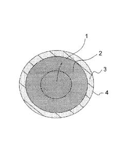
The embodiment of the insulated wire of the present invention, as shown
in the cross-sectional view in Fig. 1(a), has a conductor 1, a foamed
insulating
layer 2 covering the conductor 1, and a filled layer 4 containing a partial
discharge resistant material 3.
In another embodiment of the insulated wire of the present invention,
whose cross-sectional view is shown in Hg. 1(b), the conductor having a
rectangular cross-section is used as the conductor 1, and other parts of the
configuration are basically the same as the configuration shown in Fig. 1(a).
Since the cross-section of the conductor 1 is rectangular, the foamed
insulating
layer 2 and the filled layer 4 containing the partial discharge resistant
material 3
also have rectangular cross-sections.
CA 2864229 2017-10-05
CA 02864229 2014-08-08
8
In still another embodiment of the insulated wire of the present invention,
whose cross-sectional view is shown in Fig. 2(a), the configuration of the
insulated wire is the same as that shown in Fig. 1(a), except that a filled
layer 25
is provided on the outer circumference of the conductor 1 and at the inner
side of
the foamed insulating layer 2. In still another embodiment of the insulated
wire
of the present invention shown in Fig. 2(b), the configuration is equivalent
to a
form in which the foamed insulating layer 2 of Fig. 2(a) is divided into
plural layers
and laminated, by having a filled layer 26 that is concentric with the foamed
insulating layer 2, within the foamed insulating layer 2 provided at the outer
side
of the conductor 1 having the filled layer 25 provided on the outer
circumference.
In the present specification, a filled layer means a layer that is not foamed.
In
the Figures shown above, the same reference symbols respectively mean the
same members, and further description will not be repeated herein.
{0017}
As such, when the insulated wire has a filled layer on both or one of the
inner circumference and the outer circumference of the foamed insulating
layer,
the adhesiveness between the conductor and the insulating layer, and the
mechanical strength is increased, which is more preferable. However, in this
case, it is preferable that the thickness of the foamed insulating layer be
30% to
90% of the sum of the thickness of the foamed insulating layer and the
thickness
of the filled layer, so as not to interrupt the effect of decreasing the
relative
dielectric constant. In a case where the proportion of the thickness of the
foamed insulating layer is too low, the resistance to partial discharge is
deteriorated. Therefore, the proportion of the thickness is determined in
consideration of this.
The partial discharge resistant material refers to an insulating material
that is not susceptible to partial discharge deterioration, and a material has
an
action of enhancing the characteristic of life in charged state by dispersing
the
CA 02864229 2014-08-08
9
material in the insulating film of the wire. Examples thereof include oxides
(oxides of metals or non-metal elements), nitrides, glass and mica, and
specific
examples of the partial discharge resistant material 3 that can be used
include
microparticles of silica, titanium dioxide, alumina, barium titanate, zinc
oxide, and
gallium nitride. More preferred examples include silica and titanium dioxide.
The grain size of primary particles of the microparticles is preferably 1 pirn
or less,
and more preferably 500 nm or less. There is no limitation on the lower limit,
but
the lower limit is usually 1 nm.
When the grain size of the partial discharge resistant material is set within
the range described above, there is available an operating effect that the
life in
charged state of the wire is enhanced. In a case where the grain size is too
large, the effect of increasing the life in charged state is small, the
surface
flatness or flexibility of the insulating film is deteriorated, and in a case
where the
grain size is too small, it is difficult to obtain the effect of micronization
by
aggregation.
{0018}
The content of the partial discharge resistant material in the filled layer
that is not foamed and is disposed on the outer circumference of the foamed
insulating layer is determined from the viewpoint of the intended operating
effect.
Preferably, the content is 30% by mass or less, and more preferably 20% to 30%
by mass, relative to the amount of the resin that constitutes the filled
layer. The
content is determined so as to obtain an effect that the resistance to partial
discharge is increased to a large extent while flexibility is maintained. In a
case
where the content of the partial discharge resistant material is too large, a
problem occurs that flexibility of the insulating film is deteriorated, and in
a case
where the content is too small, the effect of increasing the life in charged
state is
decreased.
The insulated wire may have a filled layer on the inner circumference of
CA 02864229 2014-08-08
the foamed insulating layer, or the foamed insulating layer may be configured
as
a laminate of plural foamed layers each having a filled layer on both or one
of the
inner circumference and the outer circumference. The partial discharge
resistant material may be contained in the foamed insulating layer and/or the
5 filled layer on the inner circumference of the foamed insulating layer.
That is, the
partial discharge resistant material may be contained in the filled layer on
the
outer circumference and the filled layer on the inner circumference, or may be
contained in the filled layer on the outer circumference and the foamed
insulating
layer, or may be contained in all of the filled layer on the outer
circumference, the
10 filled layer on the inner circumference, and the foamed insulating
layer. The
amount of the partial discharge resistant material in this case is preferably
5% to
30% relative to the amount of the resin in the foamed insulating layer, and in
the
filled layer on the inner circumference of the foamed insulating layer, the
amount
is 30% by mass or less, and more preferably in the range of 20% to 30% by
mass,
relative to the amount of the resin. From the viewpoints of dielectric
constant
and flexibility, it is preferable that the partial discharge resistant
material be
contained only in the filled layers on the inner circumference and the outer
circumference, and from the viewpoint of effectively exhibiting the resistance
to
partial discharge, it is particularly preferable that the partial discharge
resistant
material be contained only in the filled layer on the outer circumference.
Furthermore, a filled layer containing no partial discharge resistant
material may be applied on the further outer circumference of the filled layer
on
the outer circumference containing the partial discharge resistant material,
that is,
on the outermost circumference of the insulated wire. An insulated wire
configured as such has satisfactory surface flatness and excellent sliding
properties. In this case, in order not to damage the resistance to partial
discharge and the characteristic of dielectric constant, the thickness of the
filled
layer containing no partial discharge resistant material on the outermost
CA 02864229 2014-08-08
11
circumference is preferably 5% to 10% of the overall thickness.
{0019}
The conductor 1 is made of, for example, copper, a copper alloy,
aluminum, an aluminum alloy, or a combination thereof. The cross-sectional
shape of the conductor 1 is not limited, and a circular shape, a rectangular
shape
(perpendicular shape), and the like can be applied.
{0020}
Materials for preparing the foamed insulating layer 2 is preferably capable
of being varnish state material, which can be be applied and baked on a
conductor thereby to form an insulating film. For example, polyether imide
(PEI),
polyether sulfone (PES), polyimide (PI), and polyannideimide (PAI) can be
used.
More preferred examples include polyimide (PI) and polyamideimide (PAI) having
excellent solvent resistance. Meanwhile, regarding the resin used, one kind
may
be used alone, or two or more kinds may be used in mixture.
{0021}
The foamed insulating layer 2 can be obtained by applying, around the
conductor, an insulating varnish obtained by mixing an organic solvent which
is a
main solvent component of the varnish, two kinds or three or more kinds
including
at least one kind of a high boiling solvent (as will be described below, three
kinds
of an organic solvent that dissolves a thermosetting resin, a bubble
nucleating
agent as a high boiling solvent, and a foaming agent: provided that when the
high
boiling solvent plays the role of both the bubble nucleating agent and the
foaming
agent, two kinds), and baking the varnish. The varnish may be applied on the
conductor directly or via another resin layer interposed therebetween.
The foamed insulating layer 2 can be obtained by applying, around the
conductor, an insulating varnish obtained by mixing three or more kinds of
solvents including the particular organic solvent and at least one kind of a
high
boiling solvent, and baking the varnish. The varnish may be applied on the
CA 02864229 2014-08-08
12
conductor directly or via another resin layer interposed therebetween.
{0022}
The organic solvent described above acts as a solvent for dissolving the
thermosetting resin. This organic solvent is not particularly limited as long
as the
organic solvent does not inhibit the reaction of the thermosetting resin, and
examples thereof include amide-based solvents such as N-methyl-2-pyrrolidone
(NMP), N,N-dimethylacetamide (DMAC), and N,N-dimethylformamide; urea-
based solvents such as N,N-dimethylethyleneurea, N,N-dimethylpropyleneurea,
and tetramethylurea; lactone-based solvents such as y-butyrolactone and y-
caprolactone; carbonate-based solvents such as propylene carbonate; ketone-
based solvents such as methyl ethyl ketone, methyl isobutyl ketone, and
cyclohexanone; ester-based solvents such as ethyl acetate, n-butyl acetate,
butyl
cellosolve acetate, butyl carbitol acetate, ethyl cellosolve acetate, and
ethyl
carbitol acetate; glyme-based solvents such as diglyme, triglyme, and
tetraglyme;
hydrocarbon-based solvents such as toluene, xylene, and cyclohexane; and
sulfone-based solvents such as sulfolane. Among these, in view of high
solubility, high reaction promotion properties or the like, an amide-series
solvent
or a urea-series solvent is preferred; and in view of having no hydrogen atom
that
is apt to inhibit a crosslinking reaction due to heating or the like, N-methy1-
2-
pyrrolidone, N,N-dimethylacetamide, N,N-dimethylethyleneurea, N,N-
dimethylpropyleneurea or tetramethylurea is further preferred, and N-methy1-2-
pyrrolidone is particularly preferred. The boiling point of this organic
solvent is
preferably 160 C to 250 C, and more preferably 165 C to 210 C.
{0023}
The high boiling solvent that can be used for bubble formation is a solvent
having a boiling point of preferably 180 C to 300 C, and more preferably 210 C
to 260 C. Specific examples that can be used for bubble formation include
diethylene glycol dimethyl ether, triethylene glycol dimethyl ether,
diethylene
CA 02864229 2014-08-08
13
glycol dibutyl ether, tetraethylene glycol dimethyl ether, and tetraethylene
glycol
monomethyl ether. From the viewpoint of having a smaller fluctuation in the
bubble size, triethylene glycol dimethyl ether is more preferred. Furthermore,
the examples that can be used for bubble formation include diethylene glycol
dimethyl ether, dipropylene glycol dimethyl ether, diethylene glycol ethyl
methyl
ether, dipropylene glycol monomethyl ether, diethylene glycol diethyl ether,
diethylene glycol monomethyl ether, diethylene glycol butyl methyl ether,
tripropylene glycol dimethyl ether, triethylene glycol dimethyl ether,
diethylene
glycol monobutyl ether, ethylene glycol monophenyl ether, triethylene glycol
monomethyl ether, diethylene glycol dibutyl ether, triethylene glycol butyl
methyl
ether, polyethylene glycol dimethyl ether, tetraethylene glycol dimethyl
ether,
polyethylene glycol monomethyl ether, and propylene glycol monomethyl ether.
Among them, tetraethylene glycol dimethyl ether, diethylene glycol dibutyl
ether,
triethylene glycol dimethyl ether, diethylene glycol diethyl ether,
triethylene glycol
monomethyl ether and the like are preferred as a bubble nucleating agent.
Preferred combinations of at least two kinds of the high boiling solvents
include
tetraethylene glycol dimethyl ether with diethylene glycol dibutyl ether,
diethylene
glycol dibutyl ether with triethylene glycol dimethyl ether, triethylene
glycol
monomethyl ether with tetraethylene glycol dimethyl ether, and triethylene
glycol
butyl methyl ether with tetraethylene glycol dimethyl ether. More preferred
combinations include diethylene glycol dibutyl ether with triethylene glycol
dimethyl ether, and triethylene glycol monomethyl ether with tetraethylene
glycol
dimethyl ether.
The high boiling solvent for bubble formation needs to have a boiling
.. point higher than that of the solvent for dissolving the thermosetting
resin, and in
a case where one kind of the high boiling solvent is added to the varnish, it
is
preferable that the boiling point of the high boiling solvent be higher by 10
C or
more than that of the solvent for dissolving the thermosetting resin.
Furthermore,
CA 02864229 2014-08-08
14
it is understood that in a case where one kind of the high boiling solvent is
used,
the high boiling solvent takes the role of both a bubble nucleating agent and
a
foaming agent. On the other hand, in a case where two or more kinds of the
high boiling solvents are used, the solvent having the highest boiling point
acts as
.. a foaming agent, and a high boiling solvent for bubble formation having a
boiling
point that is intermediate between the solvent for dissolving the
thermosetting
resin and the high boiling solvent having the highest boiling point acts as a
bubble
nucleating agent. The solvent having the highest boiling point preferably has
a
boiling point that is higher by 20 C or more, and more preferably by 30 C to
50 C,
.. than the solvent for dissolving the thermosetting resin. The high boiling
solvent
for bubble formation having the intermediate boiling point may have a boiling
point that is intermediate between the boiling point of the solvent that acts
as a
foaming agent and the boiling point of the solvent for dissolving the
thermosetting
resin, and preferably has a difference in boiling point of 10 C or more from
the
.. boiling point of the foaming agent. In a case where the high boiling
solvent for
bubble formation having the intermediate boiling point has a solubility for
the
thermosetting resin higher than that of the solvent that acts as a foaming
agent,
uniform bubbles can be formed after varnish baking.
{0024}
In the present invention, various additives such as a foam nucleating
agent, an oxidation inhibitor, an antistatic agent, an anti-ultraviolet agent,
a light
stabilizer, a fluorescent brightening agent, a pigment, a dye, a
compatibilizing
agent, a lubricating agent, a reinforcing agent, a flame retardant, a
crosslinking
agent, a crosslinking aid, a plasticizer, a thickening agent, a thinning
agent, and
an elastomer may be incorporated into the raw materials for obtaining the
foamed
insulating layer, to the extent that the characteristics are not affected.
Furthermore, a layer formed from a resin containing these additives may be
laminated on the resulting insulated wire, or the insulated wire may be coated
CA 02864229 2014-08-08
with a coating material containing these additives.
{0025}
The effective relative dielectric constant of the insulated wire is preferably
4.0 or less, further preferably 3.0 or less, so as to obtain an effect of
improving a
5 partial discharge inception voltage in the obtained insulated wire. There
are no
limitations on the lower limit of the relative dielectric constant, but the
lower limit is
preferably 1.5 or more. The relative dielectric constant can be measured using
a
commercially available measuring device. The measurement temperature and
the measurement frequency can be modified according to the necessity, but
10 unless particularly stated otherwise in the present specification,
measurement
was made by setting the measurement temperature to 25 C, while setting the
measurement frequency to 50 Hz.
{0026}
In order to realize a necessary relative dielectric constant, the foaming
15 magnification of the foamed insulating layer 2 is preferably 1.2 times
or more, and
more preferably 1.4 times or more. There are no particular limitations on the
upper limit of the foaming magnification, but it is usually preferable to set
the
foaming magnification to 5.0 times or less. The foaming magnification is
obtained by determining the density of a resin coated for foaming (pf) and the
density of the resin before foaming (ps) by the underwater replacement method,
and calculating the foaming magnification from (ps/pf).
{0027}
The foamed insulating layer 2 has an average bubble size of 5 rn or less,
preferably 3 01 or less, and further preferably 1 p.m or less. Since the
dielectric
breakdown voltage is decreased when the average bubble size exceeds 5 pm,
the dielectric breakdown voltage can be maintained finely by adjusting the
average bubble size to 5 pm or less. Furthermore, the dielectric breakdown
voltage can be retained more certainly by adjusting the average bubble size to
3
CA 02864229 2014-08-08
16
or less. Although the lower limit of the average bubble size is not limited,
it
is practical and preferable that the lower limit is 1 nm or more. Although the
thickness of the foamed insulating layer 2 is not limited, it is practical and
preferable that the thickness is from 10 to 200 ,m.
{0028}
Regarding the partial discharge resistant material 3, microparticles of
silica, titanium dioxide, alumina, barium titanate, zinc oxide, gallium
nitride and
the like can be used. More preferred examples include microparticles of silica
and titanium dioxide. The grain size of the microparticles is preferably 1 pm
or
less, and more preferably 500 nm or less.
{0029}
The filled layer 4 means a layer that does not foam in the present
invention. In order to enhance the resistance to partial discharge, the
outermost
layer of the insulating film contains the partial discharge resistant material
3.
The partial discharge resistant material may also be included in other filled
layers,
or the material may also be included in all of the layers.
EXAMPLES
{0030}
The present invention will be described in more detail based on examples
given below, but the invention is not meant to be limited by these. Meanwhile,
in
the following Examples, the percent value ( /0) indicating the composition
means
percent (%) by mass.
{0031}
Insulated wires of Examples and Comparative Examples were produced
as follows. A polyamideimide varnish used in a foamed insulating layer was
obtained by introducing 1,000 g of HI-406 (an NMP solution of 32% by mass of
the resin component) (trade name, manufactured by Hitachi Chemical Co., Ltd.)
CA 02864229 2014-08-08
17
into a separable flask having a capacity of 2 L, and adding 100 g of
triethylene
glycol monomethyl ether and 150 g of tetraethylene glycol dimethyl ether as
bubble forming agents to this solution. For a polyamideimide varnish used in a
filled layer, 1,000 g of HI-406 was used. 1,000 g of this polyamideimide
varnish
was used as a 30 mass% resin solution using NMP as a solvent.
A polyimide varnish used in the foamed insulating layer was obtained by
introducing 1,000 g of U-IMIDE (an NMP solution of 25% by mass of the resin
component) (manufactured by Unitika, Ltd., trade name) into a separable flask
having a capacity of 2 L, and adding 75 g of NMP, 150 g of DMAC, and 200 g of
tetraethylene glycol dimethyl ether thereto as solvents. The polyimide varnish
used in the filled layer was prepared by using U-IMIDE and adding 250 g of
DMAC as a solvent to 1,000 g of the resin.
The various insulating varnishes thus obtained were applied on a copper
conductor having a diameter of 1 mm il) and baked at a furnace temperature of
520 C, and thus insulated wires having film thicknesses of 26 fam to 29 rn
were
obtained. For the insulated wires thus obtained, dimension, dielectric
constant,
partial discharge inception voltage, life in charged state, heat resistance,
and
flexibility were evaluated.
{0032}
(Example 1)
An insulated wire (see Fig. 2(a)) composed of a foamed polyamideimide
layer (thickness: 18 ,m), an inner filled layer (4 m) of polyamideimide, and
an
outer filled layer (4 ilm) containing silica (grain size: 15 nm) at a
proportion of
20% in polyamideimide was obtained. The bubble size was 41.1m.
{0033}
(Example 2)
An insulated wire (see Fig. 2(a)) composed of a foamed polyamideimide
layer (thickness: 18 mill), an inner filled layer (4 p.m) of polyamideimide,
and an
CA 02864229 2014-08-08
18
outer filled layer (5 m) containing titanium dioxide (grain size: 15 nm) at a
proportion of 20% in polyamideimide was obtained. The bubble size was 4 p.m.
{0034}
(Example 3)
An insulated wire (see Fig. 2(a)) composed of a foamed polyamideimide
layer (thickness: 18 m), an inner filled layer (4 pm) of polyamideimide, and
an
outer filled layer (4 p.m) containing titanium dioxide (grain size: 15 nm) at
a
proportion of 30% in polyamideimide was obtained. The bubble size was 4 m.
{0035}
(Example 4)
An insulated wire (see Fig. 2(a)) composed of a foamed polyamideimide
layer (thickness: 10 pm), an inner filled layer (4 pm) of polyamideimide, and
an
outer filled layer (15 !Am) containing titanium dioxide (grain size: 15 nm) at
a
proportion of 30% in polyamideimide was obtained. The bubble size was 4 pm.
.. {0036}
(Example 5)
An insulated wire (see Fig. 2(a)) composed of a foamed polyamideimide
layer (thickness: 17 m), an inner filled layer (4 p.m) of polyamideimide, and
an
outer filled layer (5 pm) containing titanium dioxide (grain size: 15 nm) at a
proportion of 30% in polyamideimide was obtained. The bubble size was 2 p.m.
{0037}
(Example 6)
An insulated wire (see Fig. 2(a)) composed of a foamed polyamideimide
layer (thickness: 20 pm), an inner filled layer (4 pm) containing titanium
dioxide
(grain size: 15 nm) at a proportion of 30% in polyamideimide, and an outer
filled
layer (6 p.m) was obtained. The bubble size was 4 p.m.
{0038}
(Example 7)
CA 02864229 2014-08-08
19
An insulated wire (see Fig. 2(a)) composed of a foamed polyamideimide
layer (thickness: 20 jim) containing titanium dioxide (grain size: 15 nm) at a
portion of 30%, an inner filled layer (4 prn) of polyamideimide similarly
containing
titanium dioxide (grain size: 15 nm) at a proportion of 30%, and an outer
filled
layer (6 lirn) was obtained. The bubble size was 4 m.
{0039}
(Comparative Example 1)
An insulated wire composed of a polyamideimide layer (26 jAm) was
obtained.
{0040}
(Comparative Example 2)
An insulated wire composed of a polyamideimide layer (27 pm)
containing silica (grain size: 15 nm) at a proportion of 30% was obtained.
{0041}
(Comparative Example 3)
An insulated wire composed of a polyamideimide layer (28 tim)
containing titanium dioxide (grain size: 15 nm) at a proportion of 30% was
obtained.
{0042}
(Comparative Example 4)
An insulated wire composed of a foamed polyamideimide layer
(thickness: 18 p.m), an inner filled layer of polyamideimide (5 m), and an
outer
filled layer of polyamideimide (4 vim) was obtained.
{0043}
(Comparative Example 5)
An insulated wire composed of a foamed polyamideimide layer
(thickness: 19 pm), an inner filled layer of polyamideimide (4 i.tm), and an
outer
filled layer (4 pm) containing titanium dioxide (grain size: 15 nm) at a
proportion of
CA 02864229 2014-08-08
40% in polyamideimide was obtained. The bubble size was 4 pm.
{0044}
(Comparative Example 6)
An insulated wire composed of a foamed polyamideimide layer
5 (thickness: 5 pm), an inner filled layer of polyamideimide (4 pm), and an
outer
filled layer (20 pm) containing titanium dioxide (grain size: 15 nm) at a
proportion
of 30% in polyamideimide was obtained. The bubble size was 4 p.m.
{0045}
The configurations, properties and evaluation test results of the insulated
10 wires obtained in Examples 1 to 5 and Comparative Examples 1 to 6 are
presented in Table 1 and Table 2.
Methods for evaluation are described below.
{0046}
(Thickness and average bubble size of foamed insulating layer)
15 The thickness and average bubble size of the foamed insulating layer
were determined by observing the cross-sectional surface of the foamed wire
with
a scanning electron microscope (SEM). The average bubble size is explained in
more detail. The diameters of 20 bubbles that were arbitrarily selected from
the
cross-sectional surface observed with the SEM were determined and the average
20 value thereof was obtained.
{0047}
[Porosity]
Porosity was obtained by measuring the density of the foamed electrical
wire (pf) and the density of a wire before foaming (ps) by an underwater
replacement method, and calculating the porosity value by the ratio (pfips).
{0048}
[Relative dielectric constant]
For the relative dielectric constant, the electrostatic capacity of the
CA 02864229 2014-08-08
21
foamed wire was measured, and the relative dielectric constant obtained from
the
electrostatic capacity and the thickness of the foamed insulating layer was
taken
as the measured value. For the measurement of the electrostatic capacity, LCR
HITESTER (manufactured by Hioki E.E. Corp., Model 3532-50) was used.
{0049}
(Partial discharge inception voltage)
Specimens were prepared by combining two wires into a twisted form, an
alternating voltage with sine wave 50 Hz was applied between the respective
two
conductors twisted, and while the voltage was continuously raised, the voltage
(effective value) at which the amount of discharged charge was 10 pC was
determined. The determination temperature was set at the normal temperature.
For the determination of the partial discharge inception voltage, a partial
discharge tester (KPD2050, manufactured by Kikusui Electronics Corp.) was
used.
{0050}
[Life in charged state]
Two wires were twisted with each other, and an alternating voltage of sine
wave 10 kHz-1 kVp was applied between the respective conductors and the time
t taken until dielectric breakdown occurred was measured. The measurement
temperature was normal temperature. A wire having a time to dielectric
breakdown of 100 minutes or longer was judged to pass the test criteria.
0: 1, 000 minutes or more
0: 100 minutes or more and less than 1,000 minutes
X: 100 less than minutes
{0051}
(Heat resistance)
The wire was left to stand for 500 hours in a high temperature tank at
200 C, and the occurrence or non-occurrence of cracks in the coating film was
CA 02864229 2014-08-08
22
investigated by visual observation.
0: No crack was observed.
X: Cracks were observed.
{0052}
(Flexibility)
The occurrence or non-occurrence of cracks in the coating film was
investigated with visual observation when each wire was wound 10 times closely
around the wire itself such that the wire and the wire would be in contact.
0: No crack was observed.
X: Cracks were observed.
(Grain size)
The grain size was determined by observation using scanning electron
microscope (SEM). The diameters of 20 primary particles arbitrarily selected
were measured, and the grain size was defined as the average value of the
diameters.
(Bubble size)
The average bubble size was determined by observing a cross-section of
the foamed layer by scanning electron microscopy (SEM). To explain more
specifically about the average bubble size, the lengths of arbitrarily
selected 20
bubbles in the direction of the insulating layer thickness were measured from
a
cross-section observed by SEM, and the average bubble size was defined as the
average value of the lengths.
[Condition of baking]
The baking temperatures of the foamed insulating layers and filled layers
of various Examples and Comparative Examples are as summarized in the
following Tables 1 and 2.
{0053}
=
. .
{Table 1}
Ex 1 Ex 2 Ex 3 Ex 4 Ex 5 Ex 6 Ex 7 ,
,
Existent or non-existent of foamed
Existent Existent Existent Existent
Existent Existent Existent
insulating layer
Insulating material PAI PAI PAI PA! PI PAI
PAI
Titanium Titanium Titanium
Titanium Titanium Titanium
Partial discharge resistant material Silica
dioxide Dioxide dioxide Dioxide
Dioxide Dioxide
Content of the material above
20 20 30 30 30 30 30
(0/0)
Outer and
Layer containing the material
Outer and inner foamed
Outer Outer Outer Outer Outer
R
above
inner insulating 2
layer ' Thickness of insulating film (pm) 26 27 26
29 26 30 30
Thickness of foamed insulating
18 18 18 10 17 20 20 0
layer (pm)
.
-
Thickness of inner filled layer
iv 2
4 4 4 4 4 4
4
(Pm) 2
,
Thickness of outer filled layer
4 5 4 15 5 6
6
(pm)
Ratio of thickness of foamed
69 67 69 34 66 67 67
insulating layer (/0) -
Average bubble size (pm) 4 4 4 4 2 4
4
Porosity (/0) 42 40 42 21 39 40
40
Relative dielectric constant 2.3 2.4 2.4 3.5 2.3 2.5
2.6
Partial discharge inception voltage
670 670 660 600 690 700 690
(Vrms)
Life in charged state (minute) 0 _ 0 0 0
0
Heat resistance 0 0 0 0 0 0
0
Flexibility 0 0 0 0 0 0
0
"Ex" means Example according to the present invention.
PAI: Polyamide lmide
PI: Polyimide
.
. .
{0054}
{Table 21
C Ex 1 C Ex 2 C Ex 3 C Ex 4 C
Ex 5 C Ex 6
Existent or non-existent of foamed Non- Non- Non-
Existent Existent
Existent
insulating layer existent ' existent existent
_
Insulating material PAI PAI PAI PAI PAI PAI
-
Titanium Titanium Titanium
Partial discharge resistant material None Silica None
dioxide dioxide Dioxide
,
Content of the material above , 0 30 30 0
40 30
(%)
R
Layer containing the material
- - 26 All layers Outer layer Outer
layer .
above
.
Thickness of insulating film (pm) 26 27 28 27 27
29
_
.
Thickness of foamed insulating
None None None 5 19 4
.
layer (pm) .
¨
Thickness of inner filled layer
c
None None None 18 4 5
(pm)
.
,
Thickness of outer filled layer
None None None 4 4 20
(pm)
Ratio of thickness of foamed - - - 67 67 17
insulating layer (%)
Average bubble size (pm) 4 4 4 __
Porosity (%) 0 0 0 40 42 45
Relative dielectric constant 4.2 _ 4.3 6.5 2.3 2.3
4.5
Partial discharge inception voltage
540 540 450 700 690 520
(Vp) _
Life in charg_ed state (minute) X @ X @ @
Heat resistance 0 _ 0 0 0 0 0
Flexibility 0 _ 0 0 0 X 0
"C Ex" means Comparative Example.
PAI: Polyamide Imide
CA 02864229 2014-08-08
{0055}
As can be seen from Table 1, the enameled wires of Examples 1 to 4
each having a foamed insulating layer and a filled layer containing a partial
discharge resistant material on the outer circumference of the foamed
insulating
5 layer, were acknowledged to have a decrease in the relative dielectric
constant
caused by foaming, and an improvement in the partial discharge inception
voltage. Furthermore, the enameled wires had satisfactory life in charged
state,
heat resistance and flexibility.
Furthermore, also for the enameled wire of Example 6 having a filled
10 layer containing a partial discharge resistant material both on the
inner
circumference and the outer circumference, and the enameled wire of Example 7
containing a partial discharge resistant material on all of both the filled
layers on
the inner circumference and the outer circumference and the foamed insulating
layer, a decrease in the relative dielectric constant caused by foaming and an
15 increase in the partial discharge inception voltage were acknowledged
similarly,
and also, the life in charged state, heat resistance and flexibility were
satisfactory.
{0056}
On the other hand, as can be seen from Table 2, Comparative Example 1
have no foamed insulating layer and no filled layer containing a partial
discharge
20 .. resistant material had poor partial discharge inception voltage and life
in charged
state. Comparative Examples 2 and 3 that had a filled layer containing a
partial
discharge resistant material but had no foamed insulating layer, exhibited
poor
partial discharge inception voltages. Comparative Example 4 that had a foamed
insulating layer but had no filled layer containing a partial discharge
resistant
25 material, exhibited poor life in charged state. Comparative Example 5
that had a
foamed insulating layer and a filled layer containing a partial discharge
resistant
material but contained the partial discharge resistant material at a content
of 40%,
exhibited poor flexibility. Comparative Example 6 that had a foamed insulating
CA 02864229 2014-08-08
26
layer and a filled layer containing a partial discharge resistant material
while the
proportion of the foamed insulating layer was 17% in terms of the thickness of
layers, exhibited poor partial discharge inception voltage.
{0057}
The insulated wire of the present invention has a cross-sectional surface
for which cross-sectional views are shown in Figs. 1 and 2.
Examples 1 to 5 have cross-sections having a filled layer on the inner
side and the outer side of the foamed insulating layer, as shown in the cross-
sectional view of Fig. 2(a). The foamed wire of the present invention can be
applied to the case where the inner filled layer is not used as shown in the
cross-
sectional view in Fig. 1(a) and to a rectangular conductor 1 as shown in the
cross-sectional view in Fig. 1(b).
{0058}
The present invention is not construed to be limited by the above-
mentioned embodiments, and various modifications can be made within the
scope of the technical matter of the present invention.
INDUSTRIAL APPLICABILITY
{0059}
The present invention can be applied to an automobile, various kinds of
electrical/electronic equipments and the like, and fields requiring resistance
to
voltage and heat resistance. The insulated wire of the present invention can
be
used in a motor, a transformer and the like, and can provide high performance
electrical/electronic equipments. Particularly, the insulated wire of the
present
invention is favorable as a coil for the driving motors of HV (hybrid
vehicles) or EV
(electric vehicles).
{0060}
Having described our invention as related to the present embodiments, it
CA 02864229 2016-11-30
27
is our intention that the invention not be limited by any of the details of
the
description, unless otherwise specified, but rather be construed broadly
within its
spirit and scope as set out in the accompanying claims.
REFERENCE SIGNS LIST
{0062}
1 Conductor
2 Foamed insulating layer
3 Partial discharge resistant material
4 Filled layer