Note: Descriptions are shown in the official language in which they were submitted.
CA 02864986 2014-08-19
WO 2013/126349
PCT/US2013/026746
1
SYSTEMS AND METHODS FOR FLEXIBLE COMPONENTS, FLEXIBLE
CARDS, MULTI-LAYER BOARDS, MULTIPLE SENSOR DETECTORS,
NON-TIME SMEARING DETECTION MECHANISMS AND
ELECTROMAGNETIC FIELD GENERATORS FOR POWERED CARDS AND
DEVICES
Background of the Invention
[0001] This invention relates to powered cards and
devices and related systems.
Summary of the Invention
[0002] A card may include a dynamic magnetic
communications device, which may take the form of a
magnetic encoder or a magnetic emulator. A magnetic
encoder, for example, may be utilized to modify
information that is located on a magnetic medium, such
that a magnetic stripe reader may then be utilized to
read the modified magnetic information from the
magnetic medium. A magnetic emulator, for example, may
be provided to generate electromagnetic fields that
directly communicate data to a read-head of a magnetic
stripe reader. A magnetic emulator, for example, may
communicate data serially to a read-head of the
magnetic stripe reader. A magnetic emulator, for
CA 02864986 2014-08-19
WO 2013/126349
PCT/US2013/026746
2
example, may communicate data in parallel to a read-
head of the magnetic stripe reader.
[0003] All, or substantially all, of the front
surface, as well as the rear surface, of a card may be
implemented as a display (e.g., bi-stable, non bi-
stable, LCD, or electrochromic display). Electrodes of
a display may be coupled to one or more touch sensors,
such that a display may be sensitive to touch (e.g.,
using a finger or a pointing device) and may be further
sensitive to a location of the touch. The display may
be sensitive, for example, to objects that come within
a proximity of the display without actually touching
the display.
[0004] A dynamic magnetic stripe communications
device may be implemented on a multiple layer board
(e.g., a two-layer flexible printed circuit board). A
coil for each track of information that is to be
communicated by the dynamic magnetic stripe
communications device may then be provided by including
wire segments on each layer and interconnecting the
wire segments through layer interconnections to create
a coil. For example, a dynamic magnetic stripe
communications device may include two coils such that
two tracks of information may be communicated to two
different read-heads included in a read-head housing of
a magnetic stripe reader. A dynamic magnetic
communications device may include, for example, three
coils such that three tracks of information may be
communicated to three different read-heads included in
a read-head housing of a magnetic stripe reader.
[0005] Input and/or output devices may be included
on a card, for example, to facilitate data exchange
with the card. For example, an integrated circuit (IC)
CA 02864986 2014-08-19
WO 2013/126349
PCT/US2013/026746
3
may be included on a card and exposed from the surface
of the card. Such a chip (e.g., an EMV chip) may
communicate information to a chip reader (e.g., an EMV
chip reader). An RFID antenna or module may be
included on a card, for example, to send and/or receive
information between an RFID writer/reader and the RFID
included on the card.
[0006] One or more detectors may be provided on a
card, for example, to sense the presence of an external
object, such as a person or device, which in turn, may
trigger the initiation of a communication sequence with
the external object. The sensed presence of the
external object may then be communicated to a processor
of the card, which in turn may direct the exchange of
information between a card and the external object.
Accordingly, timing aspects of the information exchange
between an external object and the various I/O devices
provided on a card may also be determined by circuitry
(e.g., a processor) provided on a card.
[0007] The sensed presence of the external object or
device may include the type of object or device that is
detected and, therefore, may then determine the type of
communication that is to be used with the detected
object or device. For example, a detected object may
include a determination that the object is a read-head
housing of a magnetic stripe reader. Such an
identifying detection, for example, may activate a
dynamic magnetic stripe communications device so that
information may be communicated to the read-head of the
magnetic stripe reader. Information may be
communicated by a dynamic magnetic stripe
communications device, for example, by re-writing
magnetic information on a magnetic medium that is able
CA 02864986 2014-08-19
WO 2013/126349
PCT/US2013/026746
4
to be read by a magnetic stripe reader or
electromagnetically communicating data to the magnetic
stripe reader.
[0008] One or more read-head detectors, for example,
may be provided on a card. The one or more read-head
detectors may be provided as, for example, conductive
pads that may be arranged along a length of a card
having a variety of shapes. A property (e.g., a
capacitance magnitude) of one or more of the conductive
pads may, for example, change in response to contact
with and/or the presence of an object.
[0009] A card may, for example, be formed as a
laminate structure of two or more layers. A card may,
for example, include top and bottom layers of a plastic
material (e.g., a polymer). Electronics package
circuitry (e.g., one or more printed circuit boards, a
dynamic magnetic stripe communications device, a
battery, a display, a stacked-die processor, other
stacked-die components, wire-bond interconnects, ball
grid array interconnects, and buttons) may be
sandwiched between top and bottom layers of a laminate
structure of a card. A material (e.g., a polyurethane-
based or silicon-based substance) may be injected
between top and bottom layers and cured (e.g.,
solidified by an exposure to light, chemicals, or air)
to form a hardened card that may include a flexible
laminate structure having stacked structures sandwiched
between layers of laminate.
[0010] A processor, application specific integrated
circuit (ASIC), or other circuitry may, for example, be
implemented on a semiconductor die. Such a die may,
for example, be made to be thinner than its original
thickness (e.g., by utilizing a grinding and/or
CA 02864986 2014-08-19
WO 2013/126349
PCT/US2013/026746
polishing process). A die may, for example, be
modified to a thickness of between approximately 20
microns and 0.010 inches. A die may, for example, be
modified to a preferable thickness of between
5 approximately 0.00025 inches and 0.004 inches.
[0011] Modifying a thickness (e.g., via a grinding
or polishing process) of a die may, for example, render
a modified die having flexibility attributes. For
example, a thinner die may exhibit a minimum bend
radius or maximum bend angle without damaging the
components on the die. Accordingly, for example, a
flexible die may be encapsulated between two flexible
sheets of lamination to form a flexible card or device,
which may be flexed to a minimum bend radius without
damaging the die. In so doing, for example, the
flexible die may be rolled to a maximum bend angle
without damaging the die. Alternately, for example,
such flexible die may be arranged on a tape reel and
rolled for storage. Once needed, a machine (e.g., a
pick-and-place machine) may retrieve the flexible die
by unrolling the tape reel and extracting the die from
the tape reel to apply them to a mechanical carrier
(e.g., a printed circuit board).
[0012] An operation of a flexible card or device may
be altered when the card or device is flexed. For
example, bending a card or device while the card or
device is in operation may cause the card or device to
function differently (e.g., an oscillator on the card
or device may oscillate at a slightly different
frequency as compared to operation when the card or
device is not being flexed). A processor on the card
or device (e.g., a software routine executing on the
processor) may detect the change in operation and may
CA 02864986 2014-08-19
WO 2013/126349
PCT/US2013/026746
6
cause a reactive change to occur based on the change in
operation.
[0013] Alternately, for example, a piezoelectric
device may be used to detect flexing and a software
component on the card or device may drive the resultant
change in operation of a flexible card or device.
Other alternatives may, for example, use redundant
components (e.g., geographically spaced oscillators or
piezoelectric devices) to detect portions of a card or
device that are being flexed (e.g., components in the
flexed area change their operation) and other portions
of the card or device that are not being flexed (e.g.,
components in the non-flexed area do not change their
operation). Still other alternatives may, for example,
utilize thicker, non-flexible components and thinner,
flexible components and compare the difference in
operation between the flexible and non-flexible
components to detect that a card or device may be
flexing.
[0014] Decreasing a thickness of a die may, for
example, allow two or more die to be stacked on top of
one another without exceeding a height limit of the
card or device. For example, multiple die may be
ground to a thickness of between approximately 0.003
inches and 0.005 inches (e.g., approximately 0.004
inches) and may be stacked on top of one another.
Accordingly, for example, two die may be stacked
together to form a stacked assembly having a thickness
of between approximately 0.006 and 0.010 inches (e.g.,
approximately 0.008 inches). Alternately, for example,
three die may be stacked together to form a stacked
assembly having a thickness of between approximately
CA 02864986 2014-08-19
WO 2013/126349
PCT/US2013/026746
7
0.010 and 0.014 inches (e.g., approximately 0.012
inches).
[0015] Stacked die may be arranged on a mechanical
carrier (e.g., a PCB) from bottom to top in order of
decreasing diameters. For example, a bottom die may
exhibit a larger diameter than a die that is stacked on
top of the bottom die. Accordingly, for example,
interconnections (e.g., wire bonds) may be extended
from the top die to the bottom die, from the bottom die
to the underlying PCB and/or from the top die to the
underlying PCB. Alternately, for example, chip-to-chip
interconnections (e.g., flip-chip ball grid arrays) may
be used to interconnect the stacked die and/or the
underlying PCB.
[0016] A card may include a dynamic magnetic
communications device. Such a dynamic magnetic
communications device may take the form of a magnetic
encoder or a magnetic emulator. A magnetic encoder may
change the information located on a magnetic medium
such that a magnetic stripe reader may read changed
magnetic information from the magnetic medium. A
magnetic emulator may generate electromagnetic fields
that directly communicate data to a magnetic stripe
reader. Such a magnetic emulator may communicate data
serially to a read-head of the magnetic stripe reader.
A magnetic emulator may include one or more coils.
Each coil may be utilized to communicate a particular
track of magnetic stripe data to a magnetic stripe
track read-head of a magnetic stripe reader. For
example, two coils may be utilized to communicate two
tracks of magnetic stripe data to two read-heads inside
a read-head housing.
CA 02864986 2014-08-19
WO 2013/126349
PCT/US2013/026746
8
[0017] A dynamic magnetic stripe communications
device may be fabricated and assembled on one board at
one facility (e.g., as a component of a card) while a
different facility may fabricate and assemble a
different board with, for example, a card's processor,
dynamic magnetic communications device driver
circuitry, user interfaces, read-head detectors, light
emitting devices, displays, batteries, and any other
type of sensor, device, or associated circuitry. The
facility fabricating the board having a card's primary
circuitry may receive the board having the dynamic
magnetic stripe communications device from a different
facility and a battery, and may assemble the two boards
and the battery together.
[0018] The combined electronics package may then,
for example, be provided to a lamination facility for
lamination. Alternatively, for example, lamination may
occur at the facility that assembled the dynamic
magnetic stripe communications device board and the
primary circuit board together. The laminated card may
then be provided to a personalization facility for
personalization. During personalization, for example,
a customer's personal data may be placed on the
exterior of the card (e.g., printed, embossed, or laser
etched) as well as programmed into a processor's
memory.
[0019] The primary circuit boards for different
types of cards may be manufactured independently of the
dynamic magnetic communications devices. Accordingly,
different facilities may be dedicated to manufacturing
different types of cards. One facility, for example,
may be dedicated to the manufacture of primary card
boards for payment cards having displays. Another
CA 02864986 2014-08-19
WO 2013/126349
PCT/US2013/026746
9
facility, for example, may be dedicated to the
manufacture of primary card boards for security cards
not having any displays. In this manner, dynamic
magnetic stripe communications devices may be
fabricated at dedicated facilities in high volume.
These dynamic magnetic stripe communication devices may
then be shipped to the various other facilities
fabricating the primary boards for different types of
cards.
[0020] In manufacturing multiple boards dedicated to
particular functions, and later assembling these
multiple boards together, for example, the reliability
of the different boards may be tested separately before
assembling. Additionally, for example, the dynamic
magnetic communication device boards may be fabricated
in a higher volume than the boards for the circuitry of
any one card. In doing so, the costs associated with
the fabrication of dynamic magnetic communication
device boards may be decreased.
[0021] A primary circuit board may include multiple
layers (e.g., three layers) and may be configured to
support multiple devices. For example, a multi-layer
circuit board may include a processor, a display,
driving circuitry, buffer circuitry, buttons, a memory,
a battery, a radio frequency identification (REID) chip
(and associated circuitry), an integrated circuit (IC)
chip (and associated circuitry), external connectors,
ports, antennas, electromagnetic field generators (and
associated circuitry), read-head detectors and/or the
like.
[0022] The buttons (e.g., one or more buttons) may
be part of the primary circuit board and/or may be
separate components. The buttons may each be
CA 02864986 2014-08-19
WO 2013/126349
PCT/US2013/026746
associated with a different transaction account or
feature. Alternatively, for example, a card may
include a single button, but that single button may be
used to, for example, toggle between multiple products.
5 [0023] The processor may be any type of processing
device and may include on-board memory for storing
information. Any number of components may communicate
with the processor. For example, one or more displays
may be coupled to the processor. A display driver
10 circuit may be coupled between the display and the
processor. A memory may be coupled to the processor.
The memory may store data such as discretionary data
codes associated with buttons of a card. Discretionary
data codes may be recognized by remote servers to
effect particular actions. For example, a
discretionary data code may be stored in the memory and
may be used to cause a third party service feature to
be performed by a remote server.
[0024] A card may include any number of reader
communication devices. For example, a card may include
an IC chip (which may be implemented by the processor),
an RFID chip and/or a magnetic stripe communications
device. The IC chip (e.g., an EMV chip) may be used to
communicate information to an IC chip reader through a
connector (contact) or antenna (contactless). The RFID
chip may be used to communicate information to an RFID
reader via an antenna. The magnetic stripe
communications device may be included to communicate
information to a magnetic stripe reader. For example,
a magnetic stripe communications device may provide
electromagnetic signals to a magnetic stripe reader.
[0025] The multiple layer circuit board may include
read head detectors configured to sense the presence of
CA 02864986 2014-08-19
WO 2013/126349
PCT/US2013/026746
11
a magnetic stripe reader (e.g., a read-head housing of
a magnetic stripe reader). Information sensed by the
read-head detectors may be communicated to the
processor to cause the processor to communicate
information serially from electromagnetic generators to
magnetic stripe track receivers in a read-head housing
of a magnetic stripe reader. Driving circuitry may be
utilized by the processor, for example, to control the
electromagnetic generators.
[0026] A circuit board with multiple layers may
include devices distributed across the layers in order
to maintain thickness targets, avoid and/or prevent
interference between components, improve device
performance and/or the like. For example, a first
layer of a circuit board may include an RFID chip,
buttons, a processor, an IR transceiver, an application
specific integrated circuit associated with a dynamic
magnetic stripe communications device, battery pads, a
test/communication port (e.g., a JTAG port), an EMV
buffer, supporting circuitry, backers and/or the like.
A second layer may include copper supports for the
port, a copper pad operable as a die foundation for the
on-board wire bonded ASIC of the first layer, head
readers (e.g., e-sense pads), supporting circuitry,
backers and/or the like. A third layer may include an
external connector (e.g., an EMV connector), an RFID
antenna, supporting circuitry, backers and/or the like.
[0027] Each of the layers of the circuit board may
be differently shaped, include cutouts and/or may be of
different sizes. For example, the first layer of the
circuit board may be generally sized proportionally to
a card and may include cutouts (e.g., cutouts, etched
portions, and/or the like) for a magnetic stripe
CA 02864986 2014-08-19
WO 2013/126349
PCT/US2013/026746
12
communications device and a battery. A border may
remain around the cutout for the magnetic stripe
communications device. The cutout for the battery may
not include a border and may result in an "L" shaped
layer. The second layer may be a middle layer of the
circuit board that is generally sized proportionally to
a card and may include a cutout for a battery. The
second layer may be, for example, "L" shaped layer.
The third layer of the circuit board may generally be
rectangular and may be sized smaller than a card.
[0028] Prior to or during lamination, the first and
second layers may be aligned such that the magnetic
stripe communication device cutout of the first layer
is aligned to the read head detectors of the second
layer, and such that the battery cutouts of the first
and second layers are aligned. The third layer may be
positioned to overlap the first and second layers
including the battery cutout (e.g., may provide a base
for the battery), but may not extend into a region
including the cutout for the magnetic stripe
communication device and the read head detectors. The
antenna of the third layer may be along the entire
perimeter of the third layer and may be aligned so as
not to interfere with the magnetic stripe communication
device.
[0029] According to at least one example embodiment,
the first and second layer may be on opposite sides of
a top sheet, for example, a polyimide sheet. The
cutout of the first layer may be a removal and/or
absence of the first layer such that the sheet is
exposed. A magnetic stripe communications device may
be on the sheet. The third layer may be on, for
example, a separate, bottom sheet (e.g., polyimide
CA 02864986 2014-08-19
WO 2013/126349
PCT/US2013/026746
13
sheet). As one example, the second layer (e.g., a
portion of the second layer) may be directly on the
bottom sheet surface (e.g., no coverlay and/or the
like) and the third layer may be on an opposite side of
the bottom sheet from the second layer. The third
layer and the bottom sheet may be a size of a portion
of a card not including a magnetic stripe
communications device. An antenna may occupy some or
all of the bottom sheet as part of the third layer.
[0030] A multiple layer primary circuit board
configuration may decrease a circuit board thickness in
the magnetic stripe communication device region (which
may be designed as thin as possible), may increase
and/or maximize an RFID antenna size to improve
communication gain, facilitate the inclusion of three
or more reader communication devices in a single card,
and improve overall communication performance of the
reader communication devices.
[003].] Multiple boards may be soldered together.
Different boards may also be mechanically and
electrically coupled together, for example, via an
epoxy or conductive tape. The various components of a
card may be part of different circuit boards and/or
separate components attached to the circuit boards.
The separate components of each card may be, for
example, assembled onto the boards. For example, a
microprocessor die may be coupled to contacts of a
portion of a board. The electronics package may then
be laminated. Such a lamination may occur, for
example, in an Injection molding process (e.g., a
reaction injection molding process) and/or the like. A
laminate may be, for example, a silicon-based material
or a polyurethane-based material.
CA 02864986 2014-08-19
WO 2013/126349
PCT/US2013/026746
14
[0032] Cards may be personalized using various types
of wireless signals. For example, a card may include
an infrared sensor. A personalization machine may
include an IR transmitter. The IR transmitter may
communicate personal data, such as one or more credit
and/or debit card numbers, to an IR sensor located on
the card. Similarly, a visible light sensor may be
provided on a card for receiving visible light pulses
from a visible light transmitter that are Indicative of
personal data for a card. Alternatively or
additionally, for example, a wire-based signal may be
provided to a card for personalization. For example, a
card may include an IC chip that has contacts exposed
on the surface of the card. Electrical connections may
be made to such exposed contacts to provide personal
data into the chip. Contacts may be placed on the card
and connected to an embedded, non-exposed
microprocessor such that the microprocessor may receive
programming data from a wire-based connection.
[0033] An adapter may be provided that includes an
infrared or visible light transmitter. Such an adapter
may be provided over a contact for an IC chip
communications device. Accordingly, an IC chip
communications device may provide electronic signals to
program, for example, an IC-chip card. However, an
adapter may convert, for example, these electronic
signals into visible or infrared bursts of light.
Accordingly, an IC chip programmer may be utilized to
program a card having an infrared or visible light
sensor. Furthermore, for example, an adapter may be
placed over a magnetic stripe encoder or an RFID signal
generator that generates infrared or visible light
pulses in response to magnetic stripe encoding signals
CA 02864986 2014-08-19
WO 2013/126349
PCT/US2013/026746
or RFID programming signals. Where a card uses
multiple reader communication devices, a processor may
couple each device such that data may be communicated
to the card only once during personalization.
5 [0034] Systems and methods are provided for
detecting a read-head of a card reader using multiple
types of read-head sensors on a powered card.
[0035] A card may include a dynamic magnetic
communications device. Such a dynamic magnetic
10 communications device may take the form of a magnetic
encoder or an electromagnetic generator. A magnetic
encoder may change the information located on a
magnetic medium such that a magnetic stripe reader may
read changed magnetic information from the magnetic
15 medium. An electromagnetic generator may generate
electromagnetic fields that directly communicate data
to a magnetic stripe reader. Such an electromagnetic
generator may communicate data serially to a read-head
of the magnetic stripe reader.
[0036] A card may include one or more displays
(e.g., bi-stable, non bi-stable, LCD, LED, or
electrochromic displays) to display card numbers,
verification codes and/or bar codes. All, or
substantially all, of one or more surfaces of a card
may be a display. Electrodes of the display may be
coupled to one or more capacitive touch sensors such
that a display may be provided as a touch-screen
display. Any type of touch-screen display may be
utilized. Such touch-screen displays may be operable
of determining multiple points of touch. Accordingly,
a barcode may be displayed across all, or substantially
all, of a surface of a card. In doing so, computer
CA 02864986 2014-08-19
WO 2013/126349
PCT/US2013/026746
16
vision equipment such as barcode readers may be less
susceptible to errors in reading a displayed barcode.
[0037] A card may include a number of output devices
to output dynamic information. For example, a card may
include one or more RFIDs and/or IC chips to
communicate to one or more RFID readers or IC chip
readers, respectively. According to some example
embodiments, a card may include three or more different
types of output devices. A card may include devices to
receive information. For example, an RFID and IC chip
may both receive information and communicate
information to an RFID and IC chip reader,
respectively.
[0038] A device for receiving wireless information
signals may be provided. A light sensing device and/or
sound sensing device may be utilized to receive
information wirelessly.
[0039] A card may include a central processor that
communicates data through one or more output devices
simultaneously (e.g., an RFID, IC chip, and a dynamic
magnetic stripe communications device). The central
processor may receive information from one or more
input devices simultaneously (e.g., an RFID, IC chip,
dynamic magnetic stripe devices, light sensing device,
and a sound sensing device). A processor may be
coupled to surface contacts such that the processor may
perform the processing capabilities of, for example, an
EMV chip. The processor may be laminated over and not
exposed such that such a processor is not exposed on
the surface of the card.
[0040] A card may be provided with a button in which
the activation of the button causes a code to be
communicated through a dynamic magnetic stripe
CA 02864986 2014-08-19
WO 2013/126349
PCT/US2013/026746
17
communications device (e.g., the subsequent time a
read-head detector on the card detects a read-head).
The code may be indicative of, for example, a feature
(e.g., a payment feature). The code may be received by
the card via manual input (e.g., onto buttons of the
card) or via a wireless transmission (e.g., via light,
electromagnetic communications, sound, or other
wireless signals). A code may be communicated from a
webpage (e.g., via light and/or sound) to a card. A
card may include a display such that a received code
may be visually displayed to a user. In doing so, the
user may be provided with a way to select, and use, the
code via both an in-store setting (e.g., via a magnetic
stripe reader) or an online setting (e.g., by reading
the code from a display and entering the code into a
text box on a checkout page of an online purchase
transaction). According to at least one example
embodiment, the code may indicate which of multiple
buttons of a card is pressed. Such a code may be
stored in a memory of the card prior to issuance to a
user.
[0041] A remote server, such as a payment
authorization server, may receive the code and may
process a payment differently based on the code
received. For example, a code may be a security code
to authorize a purchase transaction. A code may
provide a payment feature such that a purchase may be
made with points, debit, credit, installment payments,
or deferred payments via a single payment account
number (e.g., a credit card number) to identify a user
and a payment feature code to select the type of
payment a user desires to utilize. A code may indicate
which button is pressed by a user and additional
CA 02864986 2014-08-19
WO 2013/126349
PCT/US2013/026746
18
features may be provided to a user (e.g., additional to
the payment transaction). For example, additional
features may include rewards for use of a card.
[0042] A dynamic magnetic stripe communications
device may include an electromagnetic generator that
comprises an inductor (e.g., a coil). Current may be
provided through this inductor to create an
electromagnetic field operable to communicate with the
read-head of a magnetic stripe reader. The drive
circuit may vary the amount of current travelling
through the coil such that a track of magnetic stripe
data may be communicated to a read-head of a magnetic
stripe reader. A switch (e.g., a transistor) may be
provided to enable or disable the flow of current
according to, for example, a frequency/double-frequency
(F2F) encoding algorithm. In doing so, bits of data
may be communicated.
[0043] Electronics may be embedded between two
layers of a polymer (e.g., a PVC or non-PVC polymer).
One or more liquid polymers may be provided between
these two layers. The liquid polymer(s) may, for
example, be hardened via a reaction between the
polymers (or other material), temperature, and/or via
light (e.g., an ultraviolet or blue spectrum light)
such that the electronics become embedded between the
two layers of the polymer and a card is formed.
[0044] A card may include a plurality of types of
sensors used to detect a read-head of a card reader.
The types of sensors may be, for example, capacitive,
inductive, photoelectric, sonic, magnetic and/or
thermal.
[0045] A capacitive sensor may be a low power sensor
including one or more conductive pads. An inductive
CA 02864986 2014-08-19
WO 2013/126349
PCT/US2013/026746
19
sensor may be a high power sensor including one or more
coils or portions of one or more coils. The one or
more coils may include, for example, a coil of a
dynamic magnetic stripe communications device and/or
one or more coils separate from the dynamic magnetic
stripe communications device.
[0046] Multiple types of read-head sensors may be
used to improve the reliability of read-head detection,
and to improve data security, without significantly
increasing power consumption. For example, a
capacitive sensor may detect any object in proximity to
the sensor using little or no power. An inductive
sensor may only detect objects that significantly
change a coupling between a coil (or coil portion) and
another coil (or another coil portion), and may use
relatively high power (e.g., relative to capacitive
sensing). For example, an inductive sensor may only
detect conductive materials and therefore the read-head
detection accuracy of an inductive sensor may be
greater than a capacitive sensor. Accordingly, by
activating an inductive sensor after a capacitive
sensor detects an object, and for a relatively short
period of time, a combination of sensors may be used to
decrease false read-head detections and decrease
erroneous data transmission without unduly increasing
power consumption.
[0047] In an inductive sensor, a magnitude of a
current or voltage across a detection coil may be used
to discriminate between objects detected by the
inductive sensor. For example, the greater the
conductivity of an object, the greater an increase or
decrease in the current or voltage across the detection
coil. Therefore, the inductive sensor may be used to
CA 02864986 2014-08-19
WO 2013/126349
PCT/US2013/026746
determine whether an object is an expected object based
on conductivity. For example, an inductive sensor may
detect relatively little current or voltage change in
the presence of organic matter (e.g., a finger) and
5 relatively high current or voltage change (e.g., a
decrease in current or voltage) in the presence of a
read-head. Further, a current or voltage change may be
different even between types of read-heads (e.g., due
to geometry, material types, etc.). Thus, an inductive
10 sensor may be used to detect known types of read-heads,
and detect unknown types of read-heads (e.g., skimmers)
based on a detection signal. If a detection by a card
does not match an expected detection, the card may not
energize a dynamic magnetic stripe communications
15 device to communicate data.
[0048] Additional and/or alternative sensors may be
included in a card to increase the accuracy of
detection and increase data security. For example, a
card may include a photoelectric sensor to determine
20 whether a card is within a card reader or exposed to
ambient environmental conditions.
[0049] A sequence of events may be used to increase
data security. For example, a sequence of detections
of sensors on a card may indicate whether a card
experiences an expected set of events, such as
sequential detection by different types of sensors
during a card swipe. If a sequence of detections by a
card does not match an expected sequence, the card may
not energize a dynamic magnetic stripe communications
device to communicate data.
[0050] A dynamic magnetic stripe communications
device may be implemented on a multiple layer board
(e.g., a two-layer flexible printed circuit board). A
CA 02864986 2014-08-19
WO 2013/126349
PCT/US2013/026746
21
coil for each track of information that is to be
communicated by the dynamic magnetic stripe
communications device may then be provided by including
wire segments on each layer and interconnecting the
wire segments through layer interconnections to create
a coil. For example, a dynamic magnetic stripe
communications device may include two coils such that
two tracks of information may be communicated to two
different read-heads included in a read-head housing of
a magnetic stripe reader. A dynamic magnetic
communications device may include, for example, three
coils such that three tracks of information may be
communicated to three different read-heads included in
a read-head housing of a magnetic stripe reader.
[0051] Input and/or output devices may be included
on a card, for example, to facilitate data exchange
with the card. For example, an integrated circuit (IC)
may be included on a card and exposed from the surface
of the card. Such a chip (e.g., an EMV chip) may
communicate information to a chip reader (e.g., an EMV
chip reader). An RFID antenna or module may be
included on a card, for example, to send and/or receive
information between an RFID reader and the RFID
included on the card.
[0052] One or more detectors may be provided, for
example, to sense the presence of an external object,
such as a person or device, which in turn, may trigger
a communication sequence with the external object.
Accordingly, for example, timing aspects of an
information exchange between an external object and the
various I/0 devices implemented on a card may be
determined by a processor of a card.
CA 02864986 2014-08-19
WO 2013/126349
PCT/US2013/026746
22
[0053] A sensed presence of an external object or
device may include the type of object or device that is
detected and, therefore, may then determine the type of
communication that is to be used with the detected
object or device. For example, a detected object may
include a determination that the object is a read-head
housing of a magnetic stripe reader. Such an
identifying detection, for example, may activate a
dynamic magnetic stripe communications device so that
information may be communicated (e.g.,
electromagnetically communicated) to the read-head of
the magnetic stripe reader.
[0054] One or more read-head detectors, for example,
may be provided on a card. The one or more read-head
detectors may be provided as, for example, conductive
pads that may be arranged along a length of a card
having a variety of shapes. A property (e.g., a
capacitance magnitude) of one or more of the conductive
pads may, for example, change in response to contact
with and/or the proximity of an object.
[0055] A card may, for example, be swiped across a
read-head of a magnetic stripe reader, such that a
series of conductive pads arranged along a length of
the card may be used to sequentially detect the
presence of the read-head as the read-head moves in
relation to the card. In doing so, for example, a
series of detections (e.g., the capacitance magnitude
of a series of conductive pads may increase and/or
decrease) which may be Indicative of a direction of a
card swipe, a velocity of a card swipe and/or an
acceleration of a card swipe.
[0056] In some instances, a width of a read-head may
be wider than a single conductive pad (e.g., a read-
CA 02864986 2014-08-19
WO 2013/126349
PCT/US2013/026746
23
head may span a width that may be substantially equal
to a width of two conductive pads). As a result, more
than one conductive pad may exhibit a change in
capacitance magnitude when, for example, a read-head
comes into contact with two or more conductive pads or
when a read-head is positioned proximate to two or more
conductive pads.
[0057] Nevertheless, rules may be implemented, for
example, whereby a property change (e.g., an increased
and/or decreased capacitance magnitude) detected in any
one conductive pad during a first measurement period
may not be allowed to affect a property change (e.g.,
an increased and/or decreased capacitance magnitude)
detected in the same conductive pad during a second
measurement period. Accordingly, for example, the
accuracy of position, velocity and/or acceleration
detections may not be affected by an analysis of
property changes induced within one conductive pad over
multiple periods of time. In so doing, a speed of a
card swipe, for example, may be increased without
sacrificing a detection accuracy of the card swipe
(e.g., without losing the ability to detect a location,
velocity and/or acceleration of a read head or contact
with a read head in relation to a card being swiped
through the read-head housing).
[0058] False alarm detection may be implemented to
reduce occurrences of false alarms. For example,
certain objects (e.g., a finger) may cause a processor
of a card to detect, for example, a presence of a read-
head housing of a magnetic stripe reader when, in fact,
no read-head housing is present. In such instances,
knowledge of, for example, a previously detected card
swipe and associated direction may allow a second
CA 02864986 2014-08-19
WO 2013/126349
PCT/US2013/026746
24
detection to be made, whereby a second read-head
detection that is consistent with the originally
detected card swipe direction may enable verification
of a legitimate card swipe and, therefore, may enable a
successful communication sequence with a magnetic
stripe reader whose presence has been detected and
verified.
[0059] For example, an analysis of a capacitance
magnitude change of one or more conductive pads of a
first row of conductive pads may be performed to
determine, for example, a presence of a read-head and a
direction of movement that the read-head exhibits
relative to the first row of conductive pads. A
subsequent analysis of a capacitance magnitude change
of one or more conductive pads along a second row of
conductive pads in the same direction as previously
detected may serve to legitimize a first detection of a
read-head and, therefore, may increase a probability
that a successful communication sequence between the
card and the magnetic stripe reader may transpire.
[0060] Systems and methods are provided for
detecting a read-head of a card reader using multiple
types of read-head sensors on a powered card.
[006].] A card may include a dynamic magnetic
communications device. Such a dynamic magnetic
communications device may include a magnetic encoder or
an electromagnetic field generator. A magnetic encoder
may change the information located on a magnetic medium
such that a magnetic stripe reader may read changed
magnetic information from the magnetic medium. An
electromagnetic field generator may generate
electromagnetic fields that directly communicate data
to a magnetic stripe reader. Such an electromagnetic
CA 02864986 2014-08-19
WO 2013/126349
PCT/US2013/026746
field generator may communicate data serially to a
read-head of the magnetic stripe reader.
[0062] A card may include one or more displays
(e.g., bi-stable, non bi-stable, LCD, LED, or
5 electrochromic displays) to display card numbers,
verification codes and/or bar codes. All, or
substantially all, of one or more surfaces of a card
may be a display. Electrodes of the display may be
coupled to one or more capacitive touch sensors such
10 that a display may be provided as a touch-screen
display. Any type of touch-screen display may be
utilized. Such touch-screen displays may be operable
of determining multiple points of touch. Accordingly,
a barcode may be displayed across all, or substantially
15 all, of a surface of a card. In doing so, computer
vision equipment such as barcode readers may be less
susceptible to errors in reading a displayed barcode.
[0063] A card may include a number of output devices
to output dynamic information. For example, a card may
20 include one or more RFIDs and/or IC chips to
communicate to one or more RFID readers or IC chip
readers, respectively. According to some example
embodiments, a card may include three or more different
types of output devices. A card may include devices to
25 receive information. For example, an RFID and IC chip
may both receive information and communicate
information to an RFID and IC chip reader,
respectively.
[0064] A device for receiving wireless information
signals may be provided. A light sensing device and/or
sound sensing device may be utilized to receive
information wirelessly.
CA 02864986 2014-08-19
WO 2013/126349
PCT/US2013/026746
26
[0065] A card may include a central processor that
communicates data through one or more output devices
simultaneously (e.g., an RFID, IC chip, and a dynamic
magnetic stripe communications device). The central
processor may receive information from one or more
input devices simultaneously (e.g., an RFID, IC chip,
dynamic magnetic stripe devices, light sensing device,
and/or a sound sensing device). A processor may be
coupled to surface contacts such that the processor may
perform the processing capabilities of, for example, an
EMV chip. The processor may be laminated over and not
exposed such that such a processor is not exposed on
the surface of the card.
[0066] A card may be provided with a button in which
the activation of the button causes a code to be
communicated through a dynamic magnetic stripe
communications device (e.g., the subsequent time a
read-head detector on the card detects a read-head).
The code may be indicative of, for example, a feature
(e.g., a payment feature). The code may be received by
the card via manual input (e.g., onto buttons of the
card) or via a wireless transmission (e.g., via light,
electromagnetic communications, sound, or other
wireless signals). A code may be communicated from a
webpage (e.g., via light and/or sound) to a card. A
card may include a display such that a received code
may be visually displayed to a user. In doing so, the
user may be provided with a way to select, and use, the
code via both an in-store setting (e.g., via a magnetic
stripe reader) or an online setting (e.g., by reading
the code from a display and entering the code into a
text box on a checkout page of an online purchase
transaction). According to at least one example
CA 02864986 2014-08-19
WO 2013/126349
PCT/US2013/026746
27
embodiment, the code may indicate which of multiple
buttons of a card is pressed. Such a code may be
stored in a memory of the card prior to issuance to a
user.
[0067] A remote server, such as a payment
authorization server, may receive the code and may
process a payment differently based on the code
received. For example, a code may be a security code
to authorize a purchase transaction. A code may
provide a payment feature such that a purchase may be
made with points, debit, credit, installment payments,
or deferred payments via a single payment account
number (e.g., a credit card number) to identify a user
and a payment feature code to select the type of
payment a user desires to utilize. A code may indicate
which button is pressed by a user and additional
features may be provided to a user (e.g., additional to
the payment transaction). For example, additional
features may include rewards for use of a card.
[0068] A dynamic magnetic stripe communications
device may include an electromagnetic field generator
that comprises an inductor (e.g., a coil). Current may
be provided through this inductor to create an
electromagnetic field operable to communicate with the
read-head of a magnetic stripe reader. The drive
circuit may vary the amount of current travelling
through the coil such that a track of magnetic stripe
data may be communicated to a read-head of a magnetic
stripe reader. A switch (e.g., a transistor) may be
provided to enable or disable the flow of current
according to, for example, a frequency/double-frequency
(F2F) encoding algorithm. In doing so, bits of data
may be communicated.
CA 02864986 2014-08-19
WO 2013/126349
PCT/US2013/026746
28
[0069] Electronics may be embedded between two
layers of a polymer (e.g., a PVC or non-PVC polymer).
One or more liquid polymers may be provided between
these two layers. The liquid polymer(s) may, for
example, be hardened via a reaction between the
polymers (or other material), temperature, and/or via
light (e.g., an ultraviolet or blue spectrum light)
such that the electronics become embedded between the
two layers of the polymer and a card is formed.
[0070] A card may include a plurality of types of
sensors used to detect a read-head of a card reader.
The types of sensors may be, for example, capacitive,
inductive, photoelectric, sonic, magnetic and/or
thermal.
[0071] A capacitive sensor may be a low power sensor
including one or more conductive pads. An inductive
sensor may be a high power sensor including one or more
coils or portions of one or more coils. The one or
more coils may Include, for example, a coil of a
dynamic magnetic stripe communications device and/or
one or more coils separate from the dynamic magnetic
stripe communications device.
[0072] An electromagnetic field generator may
include a coil. According to some example embodiments,
the coil may include bonding pads, connection pads and
bonding wires. The connection pads may connect the
bonding pads, for example, on a substrate in one
direction. The bonding wire may bond to and connect
the bonding pads, for example, in a second direction.
The first and second directions may be tailored to a
desired structure and/or desired electromagnetic
characteristic. The bonding and/or connection pads may
be, for example, deposited, etched and/or the like.
CA 02864986 2014-08-19
WO 2013/126349
PCT/US2013/026746
29
According to at least one example embodiment, the
bonding and/or connection pads may be circuit traces of
a flexible printed circuit board.
[0073] According to some example embodiments, a coil
may not include a bonding wire. A coil may include
multiple substrates bonded to each other. Each
substrate may include bonding pads connected by
connection pads. The bonding pads on different
substrates may be connected using, for example, a
conductive adhesive. The connection pads may connect
the bonding pads in different directions for different
substrates. The different directions may be tailored
to a desired structure and/or electromagnetic
characteristic.
[0074] The electromagnetic field generator may
include a core material to change characteristics of
the electromagnetic field. The core material may be
coated (e.g., coated with an insulator) and/or shaped
(e.g., by beveling edges and/or forming a shaped core
material). According to at least one example
embodiment, the core material may be on connection pads
and connected to a substrate by an adhesive in spaces
between the connection pads.
[0075] The structure of the electromagnetic field
generator may be encapsulated. One or more encapsulant
materials and/or layers may be used. An encapsulating
material may be deposited, for example, before wire
bonding, after wire bonding and/or before and after
wire bonding.
[0076] A device may, for example, be formed as a
laminate structure of two or more layers. A device
may, for example, include top and bottom layers of a
plastic material (e.g., a polymer). Electronics
CA 02864986 2014-08-19
WO 2013/126349
PCT/US2013/026746
package circuitry (e.g., one or more printed circuit
boards, a dynamic magnetic stripe communications
device, a battery, a display, a stacked-die processor,
other stacked-die components, wire-bond interconnects,
5 ball grid array interconnects, and buttons) may be
sandwiched between top and bottom layers of a laminate
structure of a device. A material (e.g., a
polyurethane-based or silicon-based substance) may be
injected between top and bottom layers and cured (e.g.,
10 solidified by an exposure to light, chemicals, or air)
to form a hardened device that may include a flexible
laminate structure having stacked structures sandwiched
between layers of laminate.
[0077] A processor, application specific integrated
15 circuit (ASIC), or other circuitry may, for example, be
implemented on a semiconductor die. Such a die may,
for example, be made to be thinner than its original
thickness (e.g., by utilizing a grinding and/or
polishing process). Modifying a thickness (e.g., via a
20 grinding or polishing process) of a die may, for
example, render a modified die having flexibility
attributes. For example, a thinner die may exhibit a
minimum bend radius or maximum bend angle without
damaging the components of the die. Accordingly, for
25 example, a flexible die may be encapsulated between two
flexible sheets of lamination to form a flexible
device, which may be flexed to a minimum bend radius
without damaging the die.
[0078] A component of a flexible device (e.g., a
30 thinned die) may be flexibly adhered to a flexible
substrate (e.g., a flexible printed circuit board) with
a flexible adhesive. The flexible adhesive may be non-
anaerobic and low ionic. The use of a flexible
CA 02864986 2014-08-19
WO 2013/126349
PCT/US2013/026746
31
adhesive may decrease a minimum bend radius or maximum
bend angle of a flexible device (e.g., a flexible
processor based device) by reducing the transfer of
force between the flexible substrate and the die. For
example, force transferred from a flexible substrate to
a die may be due to device bending, material
differences and/or imperfections (e.g., wrinkles) in
thin flexible substrates, for example, polyimide
substrates.
[0079] An operation of a flexible device may be
altered when the device is flexed. For example,
bending a device while the device is in operation may
cause the device to function differently (e.g., an
oscillator on the device may oscillate at a slightly
different frequency as compared to operation when the
device is not being flexed). A processor on the device
(e.g., a software routine executing on the processor),
or an application specific integrated circuit, may
detect device flexure and may alert a user as to a
degree of the flexure and/or change the operation of
flexed devices. For example, a user may be alerted to
a degree of flexure by a light source. The light
source may indicate when the flexible device exceeds
various bend angles (e.g., yellow light for potential
damage, red light for likely damage). As another
example, the operation of flexed devices may be changed
by, for example, changing an amount of current passing
through a component based on a degree of flexure to
compensate for flexure Induced changes of operation.
[0080] Flexure may be detected by a detector, for
example, a piezoelectric device, a MEMS (e.g., a MEMS
capacitor that changes capacitance during flexure),
and/or the like. According to some example
32
embodiments, a difference m operation between
components (e.g., flexible and non-flexible components)
may be used to detect that a device is being flexed.
[0081] Components may be stacked. For example,
components (e.g., stacked die) may be arranged on a
flexible substrate (e.g., a PCB) from bottom to top in
order of decreasing diameters. A bottom component may
exhibit a larger diameter than a component that is
stacked on top of the bottom component.
Interconnections (e.g., wire bonds) may be extended
from the top component to the bottom component, from
the bottom component to the underlying PCB and/or from
the top component to the underlying PCB. According to
some example embodiments, chip-to-chip interconnections
(e.g., flip-chip ball grid arrays) may be used to
interconnect the stacked components and/or the
underlying PCB.
[0082] Stacked components may be flexibly adhered
to each other with a flexible, low-ionic, non-anaerobic
adhesive. The use of a flexible adhesive may decrease a
minimum bend radius or maximum bend angle of a flexible
device by reducing the transfer of force between the
stacked components, and between the stacked components
and a flexible substrate.
[0082a] According to at least one example
embodiment, a method, comprising: detecting, by a card,
an object with a capacitive sensor; activating an
inductive sensor; and detecting conductivity, by the
card, using the inductive sensor.
CA 2864986 2019-04-10
32a
[0082b] According to at least one example
embodiment, a card, comprising: a capacitive sensor
operable to detect an external object; an inductive
sensor operable to detect conductivity of the external
object; and a processor operable to communicate data
based on the detection of the external object and the
conductivity of the external object.
Brief Description of the Drawings
[0083] The principles and advantages of the present
invention can be more clearly understood from the
following detailed description considered in
conjunction with the following drawings, in which the
same reference numerals denote the same structural
elements throughout, and in which:
CA 2864986 2019-04-10
CA 02864986 2014-08-19
WO 2013/126349
PCT/US2013/026746
33
[0084] FIG. 1 is an illustration of a card
constructed in accordance with the principles of the
present invention;
[0085] FIG. 2 is an illustration of a card
constructed in accordance with the principles of the
present invention;
[0086] FIG. 3 is an illustration of a card
constructed in accordance with the principles of the
present invention;
[0087] FIG. 4 is an illustration of a system
constructed in accordance with the principles of the
present invention;
[0088] FIG. 5 is an illustration of a system
constructed in accordance with the principles of the
present invention;
[0089] FIG. 6 is an illustration of process flow
charts constructed in accordance with the principles of
the present invention;
[0090] FIG. 7 shows cards and architectures
constructed in accordance with the principles of the
present invention;
[0091] FIGS. 8-10 show card layers constructed in
accordance with the principles of the present
invention;
[0092] FIG. 11 shows overlaid card layers
constructed in accordance with the principles of the
present invention;
[0093] FIG. 12 and 13 show cards in accordance with
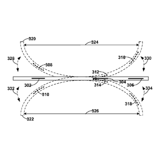
the principles of the present invention;
[0094] FIG. 14 is an illustration of a card and
architecture constructed in accordance with the
principles of the present invention;
CA 02864986 2014-08-19
WO 2013/126349
PCT/US2013/026746
34
[0095] FIG. 15 is an illustration of a card
constructed in accordance with the principles of the
present invention;
[0096] FIG. 16 is an illustration of a capacitive
read-head sensor constructed in accordance with the
principles of the present invention;
[0097] FIG. 17 is an illustration of an inductive
read-head sensor constructed in accordance with the
principles of the present invention;
[0098] FIG. 18 is an illustration of an inductive
read-head sensor constructed in accordance with the
principles of the present invention;
[0099] FIG. 19 is an illustration of a card
constructed in accordance with the principles of the
present invention;
[0100] FIG. 20 is an illustration of a process flow
in accordance with the principles of the present
invention; and
[0101] FIG. 21 is an illustration of an inductive
read-head sensor constructed in accordance with the
principles of the present invention;
[0102] FIG. 22 is an illustration of a card
constructed in accordance with the principles of the
present invention;
[0103] FIG. 23 is an illustration of a card
constructed in accordance with the principles of the
present invention;
[0104] FIG. 24 is an illustration of circuitry, and
associated waveforms, constructed in accordance with
the principles of the present invention;
[0105] FIG. 25 is an illustration of a card
constructed in accordance with the principles of the
present invention;
CA 02864986 2014-08-19
WO 2013/126349
PCT/US2013/026746
[0106] FIG. 26 is an illustration of a card
constructed in accordance with the principles of the
present invention;
[0107] FIG. 27 is an illustration of process flow
5 charts constructed in accordance with the principles of
the present invention;
[0108] FIG. 28 shows a card and architecture
constructed in accordance with the principles of the
present invention;
10 [0109] FIG. 29 shows a plan view of electromagnetic
field generators constructed in accordance with the
principles of the present invention;
[0110] FIG. 30 shows a cross-sectional view taken
along line of FIG. 23;
15 [0111] FIG. 31 shows plan views of electromagnetic
field generators constructed in accordance with the
principles of the present invention;
[0112] FIG. 32 shows a cross-sectional view of an
electromagnetic field generator constructed in
20 accordance with the principles of the present
invention;
[0113] FIG. 33 shows plan views of electromagnetic
field generators constructed in accordance with the
principles of the present invention;
25 [0114] FIG. 34 shows a partial cross-section of an
electromagnetic field generator constructed in
accordance with the principles of the present
invention;
[0115] FIG. 35 shows partial cross-sections of
30 electromagnetic field generators constructed in
accordance with the principles of the present
invention;
CA 02864986 2014-08-19
WO 2013/126349
PCT/US2013/026746
36
[0116] FIG. 36 shows a cross-sectional view of an
electromagnetic field generator that may be included in
a dynamic magnetic stripe communication device
constructed in accordance with the principles of the
present invention;
[0117] FIG. 37 is an illustration of a card
constructed in accordance with the principles of the
present invention;
[0118] FIG. 38 is an illustration of a flexible
assembly constructed in accordance with the principles
of the present invention;
[0119] FIG. 39 is an illustration of a device
constructed in accordance with the principles of the
present invention;
[0120] FIG. 40 is an illustration of a flexible
assembly constructed in accordance with the principles
of the present Invention;
[0121] FIG. 41 is an illustration of a flexible
assembly constructed in accordance with the principles
of the present invention; and
[0122] FIG. 42 illustrates process flow charts
constructed in accordance with the principles of the
present invention.
Detailed Description of the Invention
[0123] FIG. 1 shows card 100 that may include, for
example, a dynamic number that may be entirely, or
partially, displayed using a display (e.g., display
106). A dynamic number may include a permanent portion
such as, for example, permanent portion 104 and a
dynamic portion such as, for example, dynamic portion
106. Card 100 may include a dynamic number having
permanent portion 104 and permanent portion 104 may be
CA 02864986 2014-08-19
WO 2013/126349
PCT/US2013/026746
37
incorporated on card 100 so as to be visible to an
observer of card 100. For example, labeling
techniques, such as printing, embossing, laser etching,
etc., may be utilized to visibly implement permanent
portion 104.
[0124] Card 100 may include a second dynamic number
that may be entirely, or partially, displayed via a
second display (e.g., display 108). Display 108 may be
utilized, for example, to display a dynamic code such
as a dynamic security code. Card 100 may also include
third display 122 that may be used to display graphical
information, such as logos and barcodes. Third display
122 may also be utilized to display multiple rows
and/or columns of textual and/or graphical information.
[0125] Persons skilled in the art will appreciate
that any one or more of displays 106, 108, and/or 122
may be implemented as a bi-stable display. For
example, information provided on displays 106, 108,
and/or 122 may be stable in at least two different
states (e.g., a powered-on state and a powered-off
state). Any one or more of displays 106, 108, and/or
122 may be implemented as a non-bi-stable display. For
example, the display is stable in response to
operational power that is applied to the non-bi-stable
display. Other display types, such as LCD or electro-
chromic, may be provided as well.
[0126] Other permanent information, such as
permanent information 120, may be included within card
100, which may include user specific information, such
as the cardholder's name or username. Permanent
information 120 may, for example, include information
that is specific to card 100 (e.g., a card issue date
and/or a card expiration date). Information 120 may
CA 02864986 2014-08-19
WO 2013/126349
PCT/US2013/026746
38
represent, for example, information that includes
information that is both specific to the cardholder, as
well as information that is specific to card 100.
[0127] Card 100 may accept user input data via any
one or more data input devices, such as buttons 110-
118. Buttons 110-118 may be included to accept data
entry through mechanical distortion, contact, or
proximity. Buttons 110-118 may be responsive to, for
example, induced changes and/or deviations in light
intensity, pressure magnitude, or electric and/or
magnetic field strength. Such information exchange may
then be determined and processed by a processor of card
100 as data input.
[0128] Card 100 may be flexible. Card 100 may, for
example, contain hardware and/or software (e.g., flex
code stored in memory 152) that when executed by a
processor of card 100 may detect when card 100 is being
flexed. Flex code 152 may, for example, provide
processor executable applications that may detect a
change in operation of card 100 based on the flexed
condition of card 100 and may alter functions of card
100 based on the detected change in operation.
[0129] FIG. 1 shows architecture 150, which may
include one or more processors (e.g., in stacked-die
processor arrangement 154). Stacked-die processor 154
may be configured to utilize external memory 152,
internal memory of stacked-die processor 154, or a
combination of external memory 152 and internal memory
for dynamically storing information, such as executable
machine language (e.g., flex code), related dynamic
machine data, and user input data values. Stacked-die
processor 154 may, for example, execute code contained
within memory 152 to detect when a card (e.g., card 100
CA 02864986 2014-08-19
WO 2013/126349
PCT/US2013/026746
39
of FIG. 1) is being flexed. The executed code may, for
example, change the operation of a card (e.g., card 100
of FIG. 1) based on the detected change in operation.
[0130] Stacked-die processor 154 may be a
combination of two or more die stacked on top of one
another. The stacked arrangement may, for example, be
attached to a mechanical carrier (e.g., a PCB) where a
bottom die may exhibit a larger diameter than a die
stacked on top of the bottom die. Accordingly, for
example, interconnections (e.g., wire bonds) may be
placed from one die to another die and/or from each die
to the underlying PCB. Alternately, for example,
stacked-die processor 154 may be a flip-chip
combination, where die-to-die and/or die-to-PCB
connections may be established using through-die
connections and associated interconnections (e.g., a
ball grid array). In so doing, for example, each of
the stacked die may exhibit the same or different
diameters.
[0131] One or more of the components shown in
architecture 150 may be configured to transmit
information to stacked-die processor 154 and/or may be
configured to receive information as transmitted by
stacked-die processor 154. For example, one or more
displays 156 may be coupled to receive data from
stacked-die processor 154. The data received from
stacked-die processor 154 may include, for example, at
least a portion of dynamic numbers and/or dynamic
codes.
[0132] One or more displays 156 may be, for example,
touch sensitive and/or proximity sensitive. For
example, objects such as fingers, pointing devices,
etc., may be brought into contact with displays 156, or
CA 02864986 2014-08-19
WO 2013/126349
PCT/US2013/026746
in proximity to displays 156. Detection of object
proximity or object contact with displays 156 may be
effective to perform any type of function (e.g.,
transmit data to stacked-die processor 154). Displays
5 156 may have multiple locations that are able to be
determined as being touched, or determined as being in
proximity to an object.
[0133] Input and/or output devices may be
implemented on architecture 150. For example,
10 integrated circuit (IC) chip 160 (e.g., an EMV chip)
may be Included within architecture 150, that may
communicate information to a chip reader (e.g., an EMV
chip reader). Radio frequency identification (RFID)
module 162 may be included within architecture 150 to
15 enable the exchange of information with an RFID
reader/writer.
[0134] Other input and/or output devices 168 may be
included within architecture 150, for example, to
provide any number of input and/or output capabilities.
20 For example, other input and/or output devices 168 may
include an audio device capable of receiving and/or
transmitting audible information.
[0135] Other input and/or output devices 168 may
include a device that exchanges analog and/or digital
25 data using a visible data carrier. Other input and/or
output devices 168 may include a device, for example,
that is sensitive to a non-visible data carrier, such
as an infrared data carrier or an electromagnetic data
carrier.
30 [0136] Persons skilled in the art will appreciate
that a card (e.g., card 100 of FIG. 1) may, for
example, contain stacked-die components on a mechanical
carrier (e.g., a PCB) other than stacked-die processor
CA 02864986 2014-08-19
WO 2013/126349
PCT/US2013/026746
41
154. RFID 162, IC chip 160, memory 153, and/or other
I/O 168 may, for example, each be implemented on a
semiconductor die. Two or more of such components may
be stacked and interconnected via wire-bonding, ball
grid array, or other connection types. Accordingly,
for example, surface area on the PCB may be conserved
by adding components in vertical fashion rather than
adding components laterally across the surface area of
the PCB.
[0137] Persons skilled in the art will further
appreciate that a card (e.g., card 100 of FIG. 1) may,
for example, be a self-contained device that derives
its own operational power from one or more batteries
158. Furthermore, one or more batteries 158 may be
included, for example, to provide operational power for
a period of time (e.g., approximately 2-4 years). One
or more batteries 158 may be included, for example, as
rechargeable batteries.
[0138] Electromagnetic field generators 170-174 may
be included within architecture 150 to communicate
information to, for example, a read-head of a magnetic
stripe reader via, for example, electromagnetic
signals. For example, electromagnetic field generators
170-174 may be included to communicate one or more
tracks of electromagnetic data to read-heads of a
magnetic stripe reader. Electromagnetic field
generators 170-174 may Include, for example, a series
of electromagnetic elements, where each electromagnetic
element may be implemented as a coil wrapped around one
or more materials (e.g., a magnetic material and/or a
non-magnetic material). Additional materials may be
placed outside the coil (e.g., a magnetic material
and/or a non-magnetic material).
CA 02864986 2014-08-19
WO 2013/126349
PCT/US2013/026746
42
[0139] Electrical excitation by stacked-die
processor 154 of one or more coils of one or more
electromagnetic elements via, for example, driving
circuitry 164 may be effective to generate
electromagnetic fields from one or more electromagnetic
elements. One or more electromagnetic field generators
170-174 may be utilized to communicate electromagnetic
information to, for example, one or more read-heads of
a magnetic stripe reader.
[0140] Timing aspects of information exchange
between architecture 150 and the various I/O devices
implemented within architecture 150 may be determined
by stacked-die processor 154. Detector 166 may be
utilized, for example, to sense the proximity and/or
actual contact, of an external device, which in turn,
may trigger the initiation of a communication sequence.
The sensed presence and/or touch of the external device
may then be communicated to a controller (e.g.,
stacked-die processor 154), which in turn may direct
the exchange of information between architecture 150
and the external device. The sensed presence and/or
touch of the external device may be effective to, for
example, determine the type of device or object
detected.
[0141] For example, the detection may include the
detection of, for example, a read-head of a magnetic
stripe reader. In response, stacked-die processor 154
may activate one or more electromagnetic field
generators 170-174 to initiate a communications
sequence with, for example, one or more read-heads of a
magnetic stripe reader. The timing relationships
associated with communications between one or more
electromagnetic field generators 170-174 and one or
CA 02864986 2014-08-19
WO 2013/126349
PCT/US2013/026746
43
more read-heads of a magnetic stripe reader may be
provided through use of the detection of the magnetic
stripe reader.
[0142] Persons skilled in the art will appreciate
that stacked-die processor 154 may provide user-
specific and/or card-specific information through
utilization of any one or more of buttons 110-118, RFID
162, IC chip 160, electromagnetic field generators 170-
174, and other Input and/or output devices 168.
[0143] FIG. 2 shows card 200. Card 200 may, for
example, include a layer of plastic (e.g., polymer
layer 202) that may be approximately between 0.003
inches and 0.007 inches (e.g., approximately 0.005
inches) thick. Card 200 may, for example, include a
layer of plastic (e.g., polymer layer 204) that may be
approximately between 0.003 inches and 0.007 inches
(e.g., approximately 0.005 inches) thick.
[0144] Card 200 may Include stacked-die components
210-218. Stacked-die components 210-218 may, for
example, include processors, ASICs, mixed-signal
devices, transistor devices, and any other device.
Stacked-die components 210-218 may, for example, be
thinned (e.g., via a grinding or polishing process).
Such a thinning process may reduce a thickness of
stacked-die components 210-218 to a thickness of
between approximately 20 microns and 0.010 inches. A
thickness of a die may be thinned to approximately
between 0.00025 inches and .008 inches (e.g.,
approximately 0.004 inches). Stacked-die components
210-218 may be attached to a mechanical carrier (e.g.,
PCB 224).
[0145] Mechanical and/or electrical interconnections
between die 210 and die 212 may, for example, include
CA 02864986 2014-08-19
WO 2013/126349
PCT/US2013/026746
44
wire-bonds 208. Mechanical and/or electrical
interconnections between die 210 and PCB 224 may, for
example, include wire-bonds 206. Mechanical and/or
electrical interconnections between die 212 and PCB 224
may, for example, include wire-bonds 226. Die 212 may
exhibit a smaller diameter as compared to die 210.
Accordingly, for example, wire-bond connections between
die 210 and 212, between die 210 and PCB 224, and
between die 212 and PCB 224 may be facilitated. A top-
down (e.g., birds-eye) view (not shown) of die 210, die
212, and PCB 224 may, for example, illustrate that
interconnect pads associated with wire bonds 206, 208,
and 226 may be staggered so as to substantially reduce
a possibility of shorting bonding wires to interconnect
pads not associated with such bonding wires.
[0146] Electrical and/or mechanical interconnections
between die 214 and die 216 may, for example, include
flip-chip solder balls 220 of a ball grid array.
Electrical and/or mechanical interconnections between
die 216 and die 218 may, for example, include flip-chip
solder balls 228 of a ball grid array. Electrical
and/or mechanical interconnections between die 214 and
PCB 224 may, for example, include flip-chip solder
balls 230 of a ball grid array. Accordingly, for
example, die 214, 216, and 218 may exhibit the same, or
different, diameters.
[0147] Through-die vias may, for example, provide
electrical connectivity between any one or more die
214-218 and PCB 224. For example, electrical signals
may be communicated between die 218 and 216, between
die 218 and 214, between die 216 and 214 and between
any one or more of die 214-218 and PCB 224 using
conductive vias that may extend through die 214-218 and
CA 02864986 2014-08-19
WO 2013/126349
PCT/US2013/026746
may be electrically interconnected via solder balls
220, 228 and/or 230 of their respective ball grid
arrays.
[0148] Card 200 may include an encapsulant, which
5 may Include a layer of material 222 (e.g., a material
formed from one or more polyurethane-based or silicon-
based substances). Material 222 may be a substance
that changes its physical state (e.g., changes from a
liquid substance to a solid substance) when cured by
10 one or more conditions (e.g., air, heat, pressure,
light, or chemicals) for a period of time.
Accordingly, for example, card 200 may be hardened, but
may remain flexible, so that card 200 may be flexed to
exhibit either of a convex or concave shape, while
15 returning to a substantially flat orientation once
flexing ceases.
[0149] FIG. 3 shows card or device 300. Card or
device 300 may, for example, be a laminated assembly,
which may include top and bottom layers of a plastic
20 (e.g., polymer top and bottom layers) with components
302, 304 and 306 encapsulated there between. An
encapsulant of card or device 300 may be cured (e.g.,
hardened) such that card or device 300 may be rigid,
yet flexible.
25 [0150] Components 302-306 may be electrical devices
(e.g., stacked or non-stacked die) and/or mechanical
devices (e.g., buttons) that may be flexible, such that
when card or device 300 is flexed, components 302-306
may also flex. Card or device 300 may, for example,
30 include other devices (not shown) that may not be
flexible. Accordingly, for example, those devices of
card or device 300 that may flex when card or device is
flexed may also change their operation as compared to
CA 02864986 2014-08-19
WO 2013/126349
PCT/US2013/026746
46
those devices that do not flex. In so doing, for
example, detectors (not shown) may be placed within
card or device 300 to detect such a change in operation
and may take some action based upon such a detected
change in operation.
[0151] Card or device 300 may be flexed in direction
328 and/or 330 to bend card or device 300 into a
concave orientation having minimum bend radius 324.
Components 302-306 may assume positions 308, 312 and
316, respectively, as a result of such flexing.
Components 302-306 may exhibit an adequately reduced
thickness (e.g., via a grinding or polishing process)
such that flexing does not destroy the operation of
components 302-306 and may or may not change the
operation of components 302-306.
[0152] Card or device 300 may be flexed in direction
332 and/or 334 to bend card or device 300 into a convex
orientation having minimum bend radius 326. Components
302-306 may assume positions 310, 314, and 318,
respectively, as a result of such flexing. Components
302-306 may exhibit an adequately reduced thickness
(e.g., via a grinding or polishing process) such that
flexing does not destroy the operation of components
302-306 and may or may not change the operation of
components 302-306.
[0153] FIG. 4 shows system 400 of a card or device,
which may include devices 402 and 404, detector 406,
processor 410, memory 408, reaction process 412, and
device 414. Devices 402 and 404 may, for example, be
devices that may be geographically spaced apart from
one another on a card or device. Devices 402 and 404
may, for example, be devices whose operation may change
when flexed. For example, devices 402 and 404 may be
CA 02864986 2014-08-19
WO 2013/126349
PCT/US2013/026746
47
provided on one or more die, where each die may exhibit
a thickness between approximately 0.00025 inches and
0.007 inches (e.g., approximately 0.004 inches).
Further, devices 402 and 404 may be mounted on a
mechanical carrier (e.g., a PCB) that may also be
flexible. Accordingly, for example, devices 402 and
404 may be flexed during operation of system 400. In
so doing, for example, the operation of devices 402 and
404 may change based upon such flexing.
[0154] Detector 406 may, for example, sample an
output of device 402 and/or device 404 to determine
whether device 402 and/or device 404 are being flexed
during operation. Device 402 and/or device 404 may,
for example, be provided as an oscillating device
(e.g., an oscillator or piezoelectric device).
Accordingly, for example, an oscillation frequency of
such devices may change and such a change In
oscillation frequency may be detected by detector 406.
[0155] The detected change in operation may, for
example, be reported to processor 410, which may be
executing code (e.g., flex code), which may be resident
within memory 408. Accordingly, for example, a
software process (e.g., reaction process 412) executing
on processor 410 may receive a detected change in
operation from detector 406 that may be based upon a
detected flexing of system 400 (e.g., the operation of
device 402 and/or device 404 may change when a card or
device Is flexed) and may initiate a reaction (e.g., a
reaction initiated by reaction process 412) that may be
based upon the detected change in operation. Reaction
process 412 may, for example, control an operation of
device 414 based upon the detected change in operation
of device 402 and/or device 404.
CA 02864986 2014-08-19
WO 2013/126349
PCT/US2013/026746
48
[0156] A geographic separation of device 402 and
device 404 on a card or device may, for example, allow
detector 406 to determine whether specific geographic
regions of a card or device are being flexed. For
example, detector 406 may detect a change in operation
of device 402, but may detect no change in operation of
device 404 while the card or device is being flexed.
Accordingly, for example, reaction process 412, as
executed by processor 410, may determine that the
geographic region of device 402 is being flexed while
the geographic region of device 404 is not being
flexed. In so doing, for example, reaction process 412
may effect a change in operation of a device (e.g.,
device 414) based upon a change in operation of device
402.
[0157] In an alternate example, device 402 and
device 404 may exist in the same geographic region of a
card or device. Device 402 may, for example, be a non-
flexible device. Device 404 may, for example, be a
flexible device. Accordingly, for example, while a
card or device is being flexed, an operation of device
402 may not change while an operation of device 404 may
change. Such a difference in operation may be detected
by detector 406. In so doing, for example, reaction
process 412, as executed by processor 410, may
determine that a difference in operation between
devices 402 and 404 exists and may alter an operation
of a device (e.g., device 414) based upon such a
difference in operation.
[0158] FIG. 5 shows system 500 that may, for
example, provide a detected change in operation of a
flexed component (e.g., reference oscillator 502) of a
flexed card or device. System 500 may include a phase
CA 02864986 2014-08-19
WO 2013/126349
PCT/US2013/026746
49
locked loop (e.g., PLL 520) that may include
phase/frequency detector 504, charge pump 506, loop
filter 510, VCO 512, and divider 514. PLL 520 may, for
example, be implemented on a die that may not flex
(e.g., PLL 520 may be implemented on a thicker die as
compared to a thickness of a die that reference
oscillator 502 may be implemented upon). Accordingly,
for example, the operation of PLL 520 may not change
when the card or device that PLL 520 is implemented
upon may flex. Further, for example, the operation of
reference oscillator 502 may change when the card or
device that reference oscillator 502 is implemented
upon may flex.
[0159] In operation, phase/frequency detector 504
may provide signals (e.g., UP and DOWN), which may
correspond to the phase/frequency error between fREF and
f FEEDBACK = For example, if the phase/frequency of the
output of divider 514 is lagging signal fREF, then a
pulse width of signal UP may increase and a pulse width
of signal DOWN may decrease to cause the
phase/frequency of VCO 512 to be advanced in
phase/frequency. Conversely, if the phase/frequency of
the output of divider 514 is advanced with respect to
signal fRKH, then the pulse width of signal UP may
decrease and the pulse width of signal DOWN may
increase to cause the phase/frequency of VCO 512 to be
retarded in phase/frequency.
[0160] Charge pump 506 may react to signals UP
and/or DOWN by generating an error signal. For
example, if the pulse width of signal UP is increased,
the magnitude of the error signal may also increase.
If the pulse width of signal DOWN is increased, for
example, then the magnitude of the error signal may
CA 02864986 2014-08-19
WO 2013/126349
PCT/US2013/026746
also decrease. The error signal may, for example, be
filtered by loop filter 510 and provided to VCO 512 to
set the output phase/frequency, fvco, of VCO 512.
Through negative feedback, the phase/frequency error
5 between fR= and f
- FEE DBACK may be tracked and cancelled by
PLL 520.
[0161] A phase/frequency error between fREF and
f FEEDBACK may, for example, occur when a flexing of a card
or device causes reference oscillator 502 to change its
10 operation (e.g., to change a phase or frequency of
operation of reference oscillator 502). Such a
phase/frequency error may be detected by processor 516,
for example, by monitoring a magnitude of signal VERROR=
Accordingly, for example, processor 516 may detect when
15 a component of a card or device (e.g., reference
oscillator 502) changes its operation when flexed. In
so doing, for example, a software application executed
by processor 516 may receive the detected change in
operation and may implement a reactive change in
20 operation of another component (e.g., movement detector
518) of a card or device.
[0162] Movement detector 518 may include an
orientation of conductive pads, whereby one or more
conductive pads may be arranged along a length of a
25 card or device. Movement detector 518 may, for
example, detect a location of an object (e.g., a read
head of a magnetic card reader) by detecting a
characteristic change (e.g., a capacitance change) in
relation to the conductive pads of movement detector
30 518. In addition, by monitoring a characteristic
change (e.g., a capacitance change) associated with one
or more of the conductive pads and by comparing a
characteristic change of neighboring conductive pads, a
CA 02864986 2014-08-19
WO 2013/126349
PCT/US2013/026746
51
position and/or velocity and/or acceleration estimate
of an object moving in relation to such conductive pads
may be obtained.
[0163] A frequency at which a capacitance change in
the conductive pads of movement detector 518 may be
sampled may, for example, be adjusted based upon a
detected change in operation of reference oscillator
502. Accordingly, for example, if a decrease in a
phase/frequency of operation of reference oscillator
502 is detected by processor 516 in relation to a flex
event of a card or device, then processor 516 may
increase a sampling frequency of movement detector 518
to compensate. Alternately, for example, if an
increase in a phase/frequency of operation of reference
oscillator 502 is detected by processor 516 in relation
to a flex event of a card or device, then processor 516
may decrease a sampling frequency of movement detector
518 to compensate.
[0164] A flow diagram of process sequences is shown
in FIG. 6. Step 611 of sequence 610 may, for example,
reduce a thickness of one or more die by utilizing a
thinning process (e.g., a grinding or polishing
process). A thickness of a die may, for example, be
reduced to approximately between 20 microns and 0.010
inches (e.g., approximately 0.004 inches). Such a
reduced thickness die may, for example, contain
components such as processors, ASICs, and mixed-mode
circuitry (e.g., analog and digital circuitry). Such a
reduced thickness die may, for example, exhibit
increased flexibility, such that the die may be flexed
to a minimum bend radius (e.g., rolled) or to a maximum
bend angle. Accordingly, for example, such flexible
die may be rolled onto a tape reel (e.g., as in step
CA 02864986 2014-08-19
WO 2013/126349
PCT/US2013/026746
52
612). In so doing, for example, the flexible die be
retrieved from the tape reel and placed onto a
mechanical carrier (e.g., a PCB) during a pick-and-
place production operation (e.g., as in step 613) to
produce devices, such as a powered card, a telephonic
device (e.g., a cell phone), an electronic tablet, a
watch, or any other device.
[0165] Step 621 of sequence 620 may, for example,
place reduced thickness die onto a mechanical carrier
(e.g., a PCB). One or more reduced thickness die may
be stacked onto the die placed in step 621 (e.g., as in
step 622). For example, a die containing a processor
may be placed onto a mechanical carrier (e.g., a PCB)
and another die containing an ASIC may be stacked on
top of the die containing the processor. Yet another
die (e.g., a die containing mixed-mode electronics or
other circuitry) may be stacked onto the die containing
the ASIC to yield a three-die stack. Accordingly, for
example, by stacking die, surface area of the PCB may
be conserved. Such a stacked-die arrangement may be
used to produce devices, such as a powered card, a
telephonic device (e.g., a cell phone), an electronic
tablet, a watch, or any other device. Such a stacked-
die arrangement may be encapsulated between two layers
of laminate material (e.g., polymer material), injected
with an encapsulant, and hardened to produce a rigid,
yet flexible card or device.
[0166] Each of the stacked die may be interconnected
to each other and/or one or more of the stacked die may
be interconnected to signal traces on the PCB (e.g., as
in step 623). By way of example, such interconnections
may be implemented via wire bonds, whereby wires may be
attached to interconnect pads of each die. Such wire
CA 02864986 2014-08-19
WO 2013/126349
PCT/US2013/026746
53
bonding may be facilitated by placing larger diameter
die at the bottom of the stack while placing smaller
diameter die in order of decreasing diameter on top of
the larger diameter die. In addition, interconnect
pads may be staggered (e.g., no interconnect pads of
any die or substrate may be directly adjacent to one
another from a bird's eye perspective) to reduce a
possibility that wire bonds may make electrical contact
with interconnect pads not intended for that wire bond.
Alternately, for example, each stacked die may be
substantially the same diameter and may be
interconnected to each other and the PCB using through-
die vias and ball grid array interconnections.
[0167] Step 631 of sequence 630 may, for example,
place one or more reduced thickness die onto a
mechanical carrier, such as a PCB or substrate.
Detection circuitry may, for example, monitor operation
of the reduced thickness die to detect that the
mechanical carrier (and the reduced thickness die
mounted onto the mechanical carrier) may be flexed
(e.g., as in step 633).
[0168] For example, reduced thickness die may be
placed at different geographical regions of the
mechanical carrier. Accordingly, for example, by
detecting a changed operation of a flexed die (e.g., as
in step 633), a processor may determine which
geographical location of the mechanical carrier is
being flexed.
[0169] As per another example, both a flexible die
and a non-flexible die may be placed onto a mechanical
carrier. By monitoring operation of both die, a flex
event may be detected (e.g., as in step 633) by
CA 02864986 2014-08-19
WO 2013/126349
PCT/US2013/026746
54
detecting a difference in operation between the
flexible die and the non-flexible die.
[0170] In step 634, a processor of a card or device
may react to a changed operation of a flexed die. For
example, a card or device may be flexed such that a
reference oscillator on the card or device changes
frequency. A software application executed by a
processor of the card or device may, for example, react
to the changed frequency by adjusting an operation of
another component of the card or device. As per
another example, a dynamic magnetic stripe
communications device may not communicate magnetic
stripe data having an adequate magnitude when the
associated card or device is being flexed.
Accordingly, for example, a drive current provided to
the dynamic magnetic stripe communications device may
be increased by a software application executed by a
processor of the card or device (e.g., as in step 634)
based upon the detected flexing of step 633.
[0171] FIG. 7 shows cards and architectures
according to example embodiments. Referring to FIG. 7,
card 700 may include, for example, dynamic magnetic
stripe communications device 705, one or more displays
(e.g., dynamic code display 745), permanent information
747, one or more buttons (e.g., buttons 710, 720, 730
and 735) and/or information 740. Information 740 may
be, for example, a transaction number (e.g., account
number), and may be permanent and/or information in a
display. In the case of information 740 that is
permanent, information 740 may be, for example,
printed, embossed and/or laser etched on card 700.
[0172] Permanent information 747 may include, for
example, information specific to a user (e.g., a user's
CA 02864986 2014-08-19
WO 2013/126349
PCT/US2013/026746
name and/or username) and/or information specific to a
card (e.g., a card issue date and/or a card expiration
date).
[0173] Buttons 710-735 may be mechanical buttons,
5 capacitive buttons, or a combination of mechanical and
capacitive buttons. Button 710 may be used, for
example, to communicate information through dynamic
magnetic stripe communications device 705 indicative of
a user's desire to communicate a single track of
10 magnetic stripe information. Persons skilled in the
art will appreciate that pressing a button (e.g.,
button 710) may cause information to be communicated
through device 705 when an associated read-head
detector detects the presence of a read-head of a
15 magnetic stripe reader. Buttons 720, 730 and 735 may
be utilized to communicate (e.g., after a button is
pressed and after a read-head detects a read-head of a
reader) information indicative of a user selection
(e.g., to communicate two or more tracks of magnetic
20 stripe data, to communicate different track data, to
modify tracks of data and/or the like).
[0174] Buttons 710-735 may each be used to associate
a feature to a transaction. For example, each of
buttons 710-735 may be associated to different service
25 provider applications. Each service provider
application may be associated to a different service
provider feature (e.g., different rewards). A user
may, for example, press one or more of buttons 710-735
to choose one or more features for a particular
30 transaction.
[0175] A user may associate applications to buttons
and/or features to applications, for example, on a
graphical user interface (GUI). The graphical user
CA 02864986 2014-08-19
WO 2013/126349
PCT/US2013/026746
56
interface may be, for example, an application manager
provided by one or more entities (e.g., an application
manager provider). The associations may be changed,
for example, at any time, periodically, and/or upon the
occurrence of an event. According to some example
embodiments, a user may associate applications to
buttons and/or features to applications by telephone,
by electronic mail and/or any other communication
method.
[0176] Associations between buttons and service
provider applications may be maintained by an ecosystem
provider, for example, within an ecosystem of
applications, transactional methods and types of
transactions. When a transactional method (e.g., card
700) is used by a user, the ecosystem provider may
receive transactional data and information indicative
of a button selected by the user. The ecosystem
provider may determine the identity of an application
associated to the button, and may communicate some or
all of the information and/or transactional data to the
application and/or the service provider. The service
provider and/or the application may provide a feature
associated with the application based on the
information and/or transactional data.
[0177] Different features may be provided based on
the use of different transactional methods and/or
transaction types. For example, suppose a service
provider provides a reward feature based on the use of
a particular payment method (e.g., a reward for using a
particular credit card). A user may purchase an item
using the particular payment method (e.g., may select a
particular credit account using buttons 710-735). When
the purchase is performed, the reward may be
CA 02864986 2014-08-19
WO 2013/126349
PCT/US2013/026746
57
communicated to the user. As another example, suppose
a service provider provides a reward feature based on a
type of transaction. For example, a reward may be
provided for a sale of a commodity using a particular
transaction processor (e.g., issuer, acquirer and/or
payment network). A user may sell a commodity using a
the particular transaction processor (e.g., the
ecosystem provider) and upon completion of the sale a
reward may be communicated to the user.
[0178] Selection of a feature may or may not have a
cost associated with it. If a cost is associated with
the feature, for example, the cost may be added to a
customer's statement (e.g., added to a credit or debit
purchase) for a particular transaction. A fixed-fee
and/or variable-fee (e.g., a percentage of the
transaction) may then be removed from the fee charged
to the user and distributed among particular parties,
for example, distributed among a card issuer,
application manager provider, ecosystem provider,
device provider, service provider and/or one or more
other entities. Persons skilled in the art in
possession of example embodiments will appreciate that
many different fee arrangements are possible, and that
the various providers may be the same and/or different
from each other.
[0179] A cost may be associated to a feature
selection, but may not be a cost to a user. For
example, the cost may be a cost to a service provider
(e.g., a third party service provider). The cost may
be provided to other entities, for example, the device
provider, card Issuer, card processor, and/or any other
entity (e.g., a card network). For example, a feature
provided to a user acting as a merchant may be an
CA 02864986 2014-08-19
WO 2013/126349
PCT/US2013/026746
58
instant rebate provided to the customer of the user,
and a cost of the instant rebate may be a cost to the
rebate provider.
[0180] Display 745 may display, for example, a
dynamic verification code (e.g., a card verification
value (CVV) and/or card identification number (CID)).
The dynamic number displayed on display 745 may change
according to various schemes as a security measure
against fraudulent transactions. Any and/or all of the
information provided by a card 700 may be provided via
a display. For example, information 740 may be a
dynamic number provided via a display. The dynamic
numbers may change periodically and/or upon the
occurrence of an event such that a previously recorded
number may become unusable. According to at least one
example embodiment, one or both sides of a card 700 may
be entirely a display.
[0181] Card 700 and/or a user may communicate a
dynamic number to a processing facility. The
processing facility may validate the dynamic number
(e.g., a dynamic credit card number and/or a dynamic
security code). A user may purchase items using a
dynamic card and a processing facility may authorize
the purchases upon determining that the dynamic number
is valid. Although example embodiments may be
described with respect to numbers, the scope of example
embodiments includes any distinguishing representation
of a security code and/or account, by any sensory
method (e.g., sight, sound, touch and/or the like).
Characters, images, sounds, textures, letters and/or
any other distinguishable representations are
contemplated by example embodiments.
CA 02864986 2014-08-19
WO 2013/126349
PCT/US2013/026746
59
[0182] Architecture 750 may be utilized with any
card (e.g., any card 700). Architecture 750 may
include, for example, processor 755, display 757,
driving circuitry 767, memory 753, battery 760, radio
frequency identification (RFID) 765, integrated circuit
(IC) chip 763, electromagnetic field generators 773,
775, and 777, read-head detectors 770 and 780, port 787
(e.g., a joint test action group (JTAG) port), and an
RFID antenna 790.
[0183] Processor 755 may be any type of processing
device, for example, a central processing unit (CPU),
an analog signal processor and/or a digital signal
processor (DSP). Processor 755 may be, for example, an
application specific integrated circuit (ASIC).
Processor 755 may include on-board memory for storing
information (e.g., drive code). Any number of
components may communicate to processor 755 and/or
receive communications from processor 755. For
example, one or more displays (e.g., display 757) may
be coupled to processor 755. Persons skilled in the
art will appreciate that components may be placed
between particular components and processor 755. For
example, a display driver circuit may be coupled
between display 757 and processor 755.
[0184] Memory 753 may be coupled to processor 755.
Memory 753 may store data, for example, data that is
unique to a particular card. Memory 753 may store any
type of data. For example, memory 753 may store
discretionary data codes associated with each of
buttons 710-735 of card 700. Discretionary data codes
may be recognized by remote servers to effect
particular actions. For example, a discretionary data
code may be stored in memory 753 and may be used to
CA 02864986 2014-08-19
WO 2013/126349
PCT/US2013/026746
cause a third party service feature to be performed by
a remote server (e.g., a remote server coupled to a
third party service such as an online voucher and/or
coupon provider).
5 [0185] Different third party features may be, for
example, associated with different buttons and a
particular feature may be selected by pressing an
associated button. According to at least one example
embodiment, a user may select a type of payment on card
10 700 via manual input interfaces. The manual input
interfaces may correspond to displayed options (not
illustrated) and/or may be independent buttons.
Selected information may be communicated to a magnetic
stripe reader via a dynamic magnetic stripe
15 communications device, an RFID antenna and/or the like.
Selected information may also be communicated to a
device (e.g., a mobile telephonic device) including a
capacitive sensor and/or other type of touch sensitive
sensor.
20 [0186] Architecture 750 may include any number of
reader communication devices. For example,
architecture 750 may include at least one of IC chip
763, RFID 765 and a magnetic stripe communications
device. IC chip 763 may be used to communicate
25 information to an IC chip reader (not illustrated)
using, for example, RFID antenna 790 and/or contact
conductive fingers (e.g., 6 or 8 contact gold fingers).
IC chip 752 may be, for example, an EMV chip. RFID 751
may be used to communicate information to an RFID
30 reader using RFID antenna 790. RFID 751 may be, for
example, a RFID tag. A magnetic stripe communications
device may be included to communicate information to a
magnetic stripe reader. For example, a magnetic stripe
CA 02864986 2014-08-19
WO 2013/126349
PCT/US2013/026746
61
communications device may provide electromagnetic
signals to a magnetic stripe reader.
[0187] Different electromagnetic signals may be
communicated to a magnetic stripe reader to provide
different tracks of data. For example, architecture
750 may include electromagnetic field generators 773,
775 and 777 to communicate separate tracks of
information to a magnetic stripe reader.
Electromagnetic field generators 773, 775 and 777 may
include a coil (e.g., each may include at least one
coil) wrapped around one or more materials (e.g., a
soft-magnetic material and a non-magnetic material).
Each electromagnetic field generator may communicate
information, for example, serially and/or in parallel
to a receiver of a magnetic stripe reader for a
particular magnetic stripe track.
[0188] Architecture 750 may include read head
detectors 770 and 780. Read-head detectors 770 and 780
may be configured to sense the presence of a magnetic
stripe reader (e.g., a read-head housing of a magnetic
stripe reader). A read-head detector may include, for
example, e-sense pads. Information sensed by the read-
head detectors 770 and 780 may be communicated to
processor 755 to cause processor 755 to communicate
information serially from electromagnetic generators
773, 775, and 777 to magnetic stripe track receivers in
a read-head housing of a magnetic stripe reader.
[0189] According to at least one example embodiment,
a magnetic stripe communications device may change the
information communicated to a magnetic stripe reader at
any time. Processor 755 may, for example, communicate
user-specific and card-specific information using REID
765, IC chip 763, and/or electromagnetic generators
CA 02864986 2014-08-19
WO 2013/126349
PCT/US2013/026746
62
773, 775, and 777 to card readers coupled to remote
information processing servers (e.g., purchase
authorization servers). Driving circuitry 767 may be
utilized by processor 755, for example, to control
electromagnetic generators 773, 775 and 777.
[0190] Architecture 750 may Include, for example, a
light sensor (not illustrated). Architecture 750 may
receive information from a light sensor. Processor 755
may determine information received by a light sensor.
[0191] FIGS. 8-10 show card layers constructed in
accordance with the principles of the present
invention. Referring to FIG. 8, layer 800 of a printed
circuit board may include, for example, RFID antenna
805 and EMV connector 810. Layer 800 may
be about 1-
3 mils thick (a mil being 1/1000 of an inch), for
example, about 2 mils thick. Persons of ordinary skill
in the art will appreciate that layer 800 may also
include various circuit traces, fill materials,
supports, components, via connections and/or the like
which may not be illustrated for clarity of
explanation.
[0192] According to at least one example embodiment,
layer 800 may he one side of a sheet, for example, one
side of a polyimide sheet (e.g., a Kapton sheet). A
side of a sheet including REID antenna 805 and EMV
connector 810 may be a bottom layer of a printed
circuit board. A second side of the sheet may include
a different layer. The different layer (not shown)
from layer 800 may include routing traces and/or other
elements. According to at least one example
embodiment, the second side of the sheet may not
include a different layer and/or metallization (e.g.,
copper), for example, may be bare polyimide.
CA 02864986 2014-08-19
WO 2013/126349
PCT/US2013/026746
63
[0193] An RFID antenna may, for example, be a series
of conductive loops on a border of layer 800. RFID
antenna 805 may be operable to communicate information
provided by a processor externally to a distance of
about, for example, 100 millimeters. For example, a
processor may communicate with an RFID device using
RFID antenna 805. RFID antenna 805 may be utilized to
communicate, for example, payment card information
(e.g., credit card information) to a reader. Although
RFID antenna 805 is described with respect to RFID,
persons of ordinary skill in the art will appreciate
that near field communications provided by an antenna
may be used for various other technologies, for
example, contactless EMV.
[0194] RFID antenna 805 may communicate an
electromagnetic signal in response to a signal provided
by, for example, an RFID chip (e.g., an application
specific integrated circuit (ASIC) and/or the like). A
size of the conductive loops may be large (e.g., as
large as possible) and may be along edge portions of
layer 800 to maximize and/or increase a size of RFID
antenna 805. Persons of ordinary skill in the art in
possession of example embodiments will appreciate that
increased antenna size may correspond to increased
gain. RFID antenna 805 may be monostatic and/or
bistatic, and may be tuned (or tunable) to a specific
range of carrier frequencies. Although FIG. 8
illustrates a helical antenna, other configurations are
contemplated by example embodiments (e.g., patch,
crossed dipole and/or the like).
[0195] EMV connector 810 may be used to connect an
EMV chip to an external device (e.g., an EMV device).
For example, EMV connector 810 may include contact pads
CA 02864986 2014-08-19
WO 2013/126349
PCT/US2013/026746
64
and/or the like used to connect a payment card to an
EMV device during a transaction. An EMV chip (e.g., a
processor) may be connected to EMV connector 810 via
one or more circuit traces and a buffer, for example, a
buffer that provides electrostatic discharge (ESD)
protection and/or bi-directional control (not
illustrated). A card may be operable to provide
contactless EMV communications and, for example, an EMV
chip may be connected by circuit traces to RFID antenna
805 alternatively to and/or additionally to EMV
connector 810. An EMV chip may be a component added to
a circuit board including layer 800 and/or may be part
of a circuit board layer.
[0196] Referring to FIG. 9, layer 900 may include,
for example, read head detectors 905, pad 910, supports
915 and/or component cutout 920. Persons of ordinary
skill in the art will appreciate that layer 900 may
also include various circuit traces, fill materials,
supports, components, vias, via connections and/or the
like which may not be illustrated for clarity of
explanation. A thickness of layer 900 may be, for
example, about 1-4 mils (e.g., about 2 mils).
[0197] Persons skilled in the art will appreciate
that a read-head housing of a magnetic stripe reader
may be provided with one, two, or three active read-
heads that are each operable to couple with a separate
magnetic track of information. A reader may also have
more than one read-head housing and each read-head
housing may be provided with one, two, or three active
read-heads that are operable to each couple with a
separate magnetic track including information. Such
read-head housings may be provided on different
surfaces of a magnetic stripe reader. For example, the
CA 02864986 2014-08-19
WO 2013/126349
PCT/US2013/026746
read-head housings may be provided on opposite walls of
a trough sized to accept payment cards. Accordingly,
the devices on the opposite sides of the trough may be
able to read a credit card regardless of the direction
5 that the credit card was swiped.
[0198] A magnetic emulator may be provided and may
be positioned on card such that when card is swiped
through a credit card reader, the magnetic emulator
passes underneath, or in the proximity of, a read-head
10 for a particular magnetic track. An emulator may be
large enough to simultaneously pass beneath, or in the
proximity of, multiple read-heads. Information may be
transmitted, for example, serially to one or more read-
heads. Information from different tracks of data may
15 also be transmitted serially and the magnetic stripe
reader may determine the different data received by
utilizing the starting and/or ending sentinels that
define the information for each track. A magnetic
emulator may also transmit a string of leading and/or
20 ending zeros such that a magnetic reader may utilize
such a string of zeros to provide self-clocking. In
doing so, for example, information may be transmitted
serially at high speeds to a magnetic stripe reader.
For example, credit card information may be transmitted
25 to a magnetic stripe reader at speeds up to, and/or
greater than, about 30Khz.
[0199] Different emulators may be provided, and
positioned, on a card to each couple with a different
read-head and each emulator may provide different track
30 information to those different read-heads. Read-head
detectors may be utilized to detect when a read-head is
over an emulator such that an emulator is controlled by
a processor to operate when a read-head detector
CA 02864986 2014-08-19
WO 2013/126349
PCT/US2013/026746
66
detects the appropriate presence of a read-head. Power
may be saved. The read-head detector may detect how
many read-heads are reading the card and, accordingly,
only communicate with the associated emulators. Power
may be conserved.
[0200] Read-head detectors 905 may be, for example,
provided as a circuit that detects changes in
capacitance and/or mechanical coupling to a conductive
material. Read head detectors 905 may be, for example,
e-sense pads and/or the like. A processor may be
provided to, for example, receive information from
read-head detectors 905. Read head detectors 905 may
be connected to the processor via circuit traces and/or
the like.
[0201] Pad 910 may be, for example, a die foundation
of a chip. For example, pad 910 may be a copper pad
used to support a wire bonded on-board ASIC chip.
Supports 915 may be, for example, supports for an
external connector (e.g., a JTAG port). As one non-
limiting example, supports 915 may be copper pads.
Component cutout 920 may indicate the absence of
symmetry in layer 900. For example, component cutout
920 may be an area not including layer 900 (e.g., not
including layer 900 and/or a polyimide support layer).
Although example embodiments may describe a component
cutout, layer 900 may be formed without a portion
corresponding to component cutout 920, may be an
etched, milled, and/or ablated portion, and/or the
like. A component, for example, a battery, may occupy
some or all of a space provided by component cutout
920.
[0202] According to at least one example embodiment,
layer 900 may be one side of a sheet, for example, one
CA 02864986 2014-08-19
WO 2013/126349
PCT/US2013/026746
67
side of a polyimide sheet (e.g., a Kapton sheet).
Layer 900 may be a middle layer of a printed circuit
board. A different side of the sheet from the layer
900 may include a different layer, for example, a top
layer. The different layer (not shown) from layer 900
may include, for example, an infrared (IR) transceiver,
a component cutout, buttons, a processor, at least one
circuit, leads, an EMV buffer, an RF1D chip, a port
and/or a component cutout. According to at least one
example embodiment, layer 900 may be a standalone
layer, for example, the only layer of a sheet.
[0203] Referring to FIG. 10, layer 1000 may include,
for example, infrared (IR) transceiver 1005, magnetic
stripe region 1010, buttons 1015, processor 1020,
circuit 1025, leads 1030, EMV buffer 1035, RFID chip
1040, port 1045 and/or component cutout 1050. Persons
of ordinary skill in the art will appreciate that layer
1000 may also include various circuit traces, fill
materials, supports, components, via connections and/or
the like which may not be illustrated for clarity of
explanation. A thickness of layer 1000 may be, for
example, about 1-4 mils (e.g., about 2.7 mils).
[0204] IR transceiver 1005 may include, for example,
an IR emitter and an IR receiver. The IR emitter may
be, for example, a light emitting diode configured to
emit IR light upon excitation (e.g., application of a
voltage across the diode). The IR receiver may be, for
example, a transistor configured to generate a current
in the presence of IR light. For example, the IR
receiver may be a bipolar transistor. According to at
least one example embodiment, IR transceiver 1005 may
not be a transceiver and may be a transmitter-receiver.
IR transceiver 1005 may be connected to, for example,
CA 02864986 2014-08-19
WO 2013/126349
PCT/US2013/026746
68
processor 1020 via one or more circuit traces (not
illustrated). IR transceiver 1005 may communicate
information to/from an external IR reader and/or
to/from processor 1020. For example, IR transceiver
1005 may communicate a card account number to an IR
card reader.
[0205] Magnetic stripe region 1010 may Indicate the
absence of a portion of layer 1000. For example,
magnetic stripe region 1010 may indicate an area of a
sheet (e.g., a polyimide sheet) not including any
metallization (e.g., no copper, coverlay and/or the
like). As another example, magnetic stripe region 1010
may indicate the absence of any material. Although
example embodiments may include a component cutout as a
magnetic stripe region, layer 1000 may be formed
without a portion corresponding to magnetic stripe
region 1010, an etched, milled, and/or ablated portion,
and/or the like. A component, for example, a magnetic
stripe communication device, may occupy some or all of
a space provided by magnetic stripe region 1010 (e.g.
directly on a polyimide sheet).
[0206] Buttons 1015 may be mechanical buttons,
capacitive buttons, or a combination of mechanical and
capacitive buttons. Buttons 1015 may be connected to
processor 1020 via one or more circuit traces (not
illustrated).
[0207] Processor 1020 may be, for example, a central
processing unit. For example, processor 1020 may be an
ultra-low-power mixed signal microprocessor. Processor
1020 may provide various functions to a powered card
including a layer 1000. For example, a card EMV
protocol may use processor 1020. Processor 1020 may
include on-board memory for storing information (e.g.,
CA 02864986 2014-08-19
WO 2013/126349
PCT/US2013/026746
69
drive code). Any number of components may communicate
to processor 1020 and/or receive communications from
processor 1020. For example, one or more displays (not
illustrated) and/or one or more memories may be coupled
to processor 1020. Persons skilled in the art will
appreciate that components may be placed between
particular components and processor 1020. For example,
a buffer circuit may be coupled between processor 1020
and an EMV connector.
[0208] Circuit 1025 may be, for example, an ASIC.
Circuit 1025 may be associated with a magnetic stripe
communication device. Leads 1030 may be, for example,
battery terminal leads to connect a thin film, flexible
battery to power various circuits (e.g., circuitry or
components of various layers including layer 1000).
EMV buffer 1035 may be connected between, for example,
an EMV connector and processor 1020. EMV buffer 1035
may provide electrostatic discharge (ESD) protection
and/or bi-directional control. REID chip 1040 may be,
for example, connected to an REID antenna (not
illustrated) and may be operable to communicate, for
example, payment card information (e.g., credit card
information) to a reader. Port 1045 may be, for
example, a JTAG port connected to processor 1020 and/or
leads 1030 via circuit traces (not illustrated).
[0209] Component cutout 1050 may indicate the
absence of symmetry in layer 1000. For example,
component cutout 1050 may be an area not including
layer 1000. Although example embodiments may describe
a component cutout, layer 1000 may be formed without a
portion corresponding to component cutout 1050, may be
an etched or otherwise removed portion and/or the like.
CA 02864986 2014-08-19
WO 2013/126349
PCT/US2013/026746
A component, for example, a battery, may occupy some or
all of a space provided by component cutout 1050.
[0210] Persons skilled in the art in possession of
example embodiments will appreciate that components of
5 various layers of a circuit board may be distributed in
various ways and remain within the scope of example
embodiments.
[0211] According to at least one example embodiment,
layer 1000 may be one side of a sheet, for example, one
10 side of a polyimide sheet (e.g., a Kapton sheet).
Layer 1000 may be a top layer of a printed circuit
board. A different side of the sheet from the layer
1000 may include a different layer, for example, a
middle layer. The different layer (not shown) from
15 layer 1000 may include, for example, read head
detectors, one or more pads, supports and/or component
cutouts. According to at least one example embodiment,
layer 1000 may be a standalone layer, for example, the
only layer of a sheet.
20 [0212] FIG. 11 shows overlaid card layers
constructed in accordance with the principles of the
present invention. Referring to FIG. 11, a printed
circuit board may include multiple layers, for example,
three layers including magnetic stripe cutout 1105,
25 read head detectors 1110, antenna 1115, buttons 1120
and 1135, processor 1125, circuit 1130, EMV connector
1140, EMV buffer 1145, leads 1150, RFID chip 1160, port
1165 and/or component cutouts 1155. Persons of
ordinary skill in the art will appreciate that circuit
30 board 1100 may include various circuit traces, fill
materials, supports, components, via connections and/or
the like which may not be illustrated for clarity of
explanation. Components, such as a magnetic stripe
CA 02864986 2014-08-19
WO 2013/126349
PCT/US2013/026746
71
communication device, battery, backers and/or buttons,
may or may not be part of circuit board 1100 (e.g., may
be separate components).
[0213] A first layer may include, for example,
component cutouts 1105 and/or 1155, buttons 1120 and
1135, processor 1125, circuit 1130, EMV buffer circuit
1145, leads 1150, RFID chip 1160 and port 1165. A
second layer may include, for example, read head
detectors 1110, a connector (not illustrated), supports
(not illustrated) and/or component cutout 1155. A
third layer may include, for example, RFID antenna 1115
and/or EMV connector 1140.
[0214] According to at least one example embodiment,
the first and second layers may be on opposite sides of
a same sheet (e.g., a Kapton sheet). The third layer
may be on a different sheet. The different sheet may
only include the third layer and an opposite side of
the sheet from the third layer may not include
metallization (e.g., no coverlay). According to at
least one other example embodiment the opposite side of
the sheet from the third layer may include routing
traces, elements, and/or the like (e.g., a fourth
layer). According to at least one example embodiment,
each layer of a circuit board may be associated with a
different substrate layer.
[0215] Circuit board 1100 may include a cutout 1155
that may extend through the first and second layers. A
component such as a battery may be on the third layer
and pass through the first and second layers.
[0216] The third layer may extend to about a portion
of the printed circuit board 1100 including read head
detectors 1110 of the second layer and/or a magnetic
stripe communication device (not illustrated). For
CA 02864986 2014-08-19
WO 2013/126349
PCT/US2013/026746
72
example, a magnetic stripe communication device may be
a component on a polyimide sheet over read head
detectors 1110 of the second layer and in magnetic
stripe cutout 1105 of the first layer. Magnetic stripe
region 1105 may indicate, for example, the absence of
elements on the first layer opposite the read head
detectors 1110. The third layer may not extend into a
region including read head detectors 1110 and/or a
magnetic stripe communication device. According to at
least one example embodiment, a sheet including the
third layer may not extend into a region including read
head detectors 1110 and/or a magnetic stripe
communication device. The sheet may be between the
third layer and the second layer.
[0217] Accordingly, interference between an RFID
antenna 1115 and a magnetic stripe communication device
and/or read head detectors may be reduced. RFID
antenna 1115 may surround an area of a circuit board
1100 not including the magnetic stripe communication
device. A thickness of circuit board 1100 may be
reduced in an area including a magnetic stripe
communication device and a size of an RFID antenna
increased, as compared to, for example, a circuit board
not including three or more layers. Communications
using an RFID antenna 1115 and/or a magnetic stripe
communication device may be improved. For example,
circuit board 1100 may provide improved gain.
[0218] FIG. 12 shows a card in accordance with the
principles of the present invention. FIG. 12 may be an
example cross-sectional representation of a card taken
in a thickness direction. Referring to FIG. 12, a card
1200 may include, for example, first exterior layer
1210, magnetic stripe communications device 1220, first
CA 02864986 2014-08-19
WO 2013/126349
PCT/US2013/026746
73
layer 1230, second layer 1240, third layer 1250, second
exterior layer 1260, battery 1270, region 1280 and fill
1290.
[0219] Magnetic stripe communications device 1220
may be on first layer 1230 (e.g., on a sheet including
layer 1230). A thickness "g" of card 1200 may be, for
example, about 25-40 mils (25-40 thousandths of an
inch). For example, card 1200 may be about 30-33 mils
thick. Card 1200 may include layers, components and/or
the like with thicknesses "a"-"f" and "h".
[0220] Each of thicknesses "e" and "f" of exterior
layers 1210 and 1260 may be, for example, about 3-8
mils (e.g., about 6 mils). Exterior layers 1210 and
1260 may include a polymer, for example, polyethelene
terephthalate. A thickness "d" of third layer 1250 may
be about 1-3 mils (e.g., 2 mils). Thicknesses "b" and
"c" of first and second layers 1230 and 1240 combined
may be about 2-7 mils (e.g., about 4.7 mils). A
thickness "h" of battery 1270 may be about 14-20 mils
(e.g., about 17 mils).
[0221] Region 1280 may be a region including a
material (e.g., an adhesive) and/or various elements
(e.g., wire traces and/or the like). According to some
example embodiments, region 1280 may not be present or
may be present as a fill material, and first layer 1230
and/or battery 1270 may extend to first exterior layer
1210. Thickness "a" of the magnetic stripe
communications device portion 1220 may be, for example,
a thickness of thickness "g" minus the combined
thicknesses "a"-"f" and a thickness (if any) of region
1280. Fill 1290 may indicate a region of card 1200
into which the third layer 1250 does not extend. For
example, the third layer 1250 may include an REID
CA 02864986 2014-08-19
WO 2013/126349
PCT/US2013/026746
74
antenna and may not extend into a region of card 1200
including a magnetic stripe communication device 1220
or may only partially extend into a region of card 1200
including a magnetic stripe communication device 1220.
Fill 1290 may include, for example, epoxy.
[0222] As one non-limiting example, to fabricate a
card that is about 30-33 mils thick, for example,
exterior layers 1210 and 1260 may each be about 4-7
mils (e.g., 5 mils). A magnetic stripe communication
device may be about 18-22 mils. A circuit board may be
less than about 10-20 mils (e.g., less than about 16
mils). The magnetic stripe communication device may be
on a portion of a circuit board layer with a thickness
of about 1-3 mils (e.g., about 2 mils). Accordingly,
for example, an area of region 1280 between a magnetic
stripe communications device and an exterior layer may
be a thickness such that a magnetic stripe
communications device, a circuit board layer (e.g.,
layer 1240) on the magnetic stripe communication
device, and exterior layers 1210 and 1260, are together
about 30-33 mils thick. For example, region 1280 may
be about 0-10 mils thick (e.g., about 2 mils).
[0223] Persons of ordinary skill in the art will
appreciate that the relative sizes of elements shown in
FIG. 12 are representative only and depend on, for
example, specific design and/or specific components.
For example, magnetic stripe component 1220 may be
thicker than battery 1270. Further, relative
dimensioning may not be to scale in order to illustrate
relative positioning in FIG. 12.
[0224] The volume of the electronics package of a
powered card may be, for example, less than about two
tenths of a cubic square inch (e.g., about less than
CA 02864986 2014-08-19
WO 2013/126349
PCT/US2013/026746
one tenth of a cubic square inch). Such an electronics
package may include multiple flexible boards, a
battery, dynamic magnetic stripe communications device,
magnetic stripe communications device drive circuitry,
5 and multiple light emitting diodes, for example. There
may be no copper pour in card 1200. A thickness of
card 1200 may be uniform or may vary (e.g., a flexible
card).
[0225] Persons skilled in the art will appreciate
10 that a protective layer may be placed over exterior
layers 1210 and 1260. Such a layer may be about 0.5-2
mils thick (e.g., about 1 mil thick). Accordingly, for
example, the combined thickness of two protective
layers may be about 2 mils, the combined thickness of
15 two exterior layers may be about 8 mils, the thickness
of a circuit board layer including read heads may be 2
mils and the thickness of a magnetic stripe
communication device may be about 18 mils. In order to
maintain a target thickness of about 30 mils (e.g.,
20 with a maximum thickness of about 32 mils including
personalization) for a card 1200, a third layer (e.g.,
including an antenna) may not overlap a region of card
1200 including a magnetic stripe communication device.
[0226] Persons skilled in the art will appreciate
25 that different components and layers may be of
different thicknesses based on the design of a card,
and that example embodiments may be applied in a wide
variety of scenarios to maintain a critical thickness.
Persons skilled in the art will appreciate that an
30 injection molding process of a substance may allow a
substance to fill into the groove and gaps of an
electronics package such that the laminate may reside,
CA 02864986 2014-08-19
WO 2013/126349
PCT/US2013/026746
76
for example, between components of an electronics
package.
[0227] Card 1200 may include a permanent magnet that
may be, for example, provided as part of an assembled
magnetic stripe communication device 1220. First
through third layers 1230-1250 may include, for
example, capacitive read-head detectors. Battery 1270
may be any type of battery, such as, for example, a
flexible lithium polymer battery. Circuitry may be
included (not illustrated), for example, one or more
driver circuits (e.g., for a magnetic communications
device), RFIDs, IC chips, light sensors and light
receivers (e.g., for sending and communicating data via
optical information signals), sound sensors and sound
receivers, or any other component or circuitry for card
1200. Read-head detectors for detecting the read-head
of a magnetic stripe reader may be provided, for
example, on layer 1240 as capacitive touch sensors
(e.g., capacitive-sensing contact plates).
[0228] FIG. 13 shows a card in accordance with the
principles of the present invention. FIG. 13 may
include an example plan view of card 1300 including
regions 1305, 1310 and 1315, and cross-sections
corresponding to the regions.
[0229] Referring to FIG. 13, card 1300 may include
regions 1305, 1310 and 1315. Region 1305 may include,
for example, first mask 1320, first conductor 1323,
second conductor 1325, substrate 1327, third conductor
1330 and second mask 1333. Substrate 1330 may be, for
example, polyimide (e.g., Kapton). Second conductor
1325 and third conductor 1330 may be on opposite sides
of substrate layer 1330. Second conductor 1325 and
third conductor 1330 may include, for example,
CA 02864986 2014-08-19
WO 2013/126349
PCT/US2013/026746
77
electrically deposited metal (e.g., ED copper). First
conductor 1323 may be on exposed portions of substrate
1327, second conductor 1325 and third conductor 1330,
and may fill vias, depressions and/or the like. First
conductor 1323 may be, for example, metal plating
(e.g., copper plating). Mask 1320 and mask 1333 may be
on first conductor 1323. Mask 1320 and mask 1333 may
be, for example, top and bottom solder masks (e.g.,
coverlay), respectively.
[0230] Region 1310 of card 1300 may include, for
example, first mask 1335, first conductor 1355, second
conductor 1340, first substrate 1343, third conductor
1345, bonding material 1347, second substrate 1350,
fourth conductor 1353 and second mask 1357. First
substrate 1343 and second substrate 1350 may be, for
example, polyimide (e.g., Kapton). Second conductor
1340 and third conductor 1345 may be on opposite side
surfaces of first substrate 1343. Fourth conductor
1353 may be on a side surface (e.g., bottom surface) of
substrate 1350. Second conductor 1340, third conductor
1345 and fourth conductor 1353 may include, for
example, electrically deposited metal (e.g., ED
copper). Bonding material 1347 may be between
substrate 1350 and third conductor 1345. Bonding
material 1347 may be, for example, a bonding sheet.
[0231] First conductor 1355 may be on exposed
portions of substrate second conductor 1340, first
substrate 1343, third conductor 1345, bonding material
1347, second substrate 1350 and fourth conductor 1353.
First conductor 1355 may fill vias, depressions and/or
the like. First conductor 1355 may be, for example,
metal plating (e.g., copper plating). First mask 1335
and second mask 1357 may be on first conductor 1355.
CA 02864986 2014-08-19
WO 2013/126349
PCT/US2013/026746
78
First mask 1335 and second mask 1357 may be, for
example, top and bottom solder masks (e.g., coverlay),
respectively.
[0232] Region 1315 of card 1300 may include, for
example, substrate 1360, first conductor 1363, second
conductor 1365 and mask 1367. A top surface of
substrate 1360 may be exposed. Substrate 1360 may be,
for example, a polyimide. First conductor 1363 may be
on an opposite side of substrate 1360 from the exposed
top surface. First conductor 1363 may be, for example,
electrically deposited copper. Second conductor 1365
may be on first conductor 1363. Second conductor 1365
may be, for example, copper plating. Mask 1367 may be
on second conductor 1365. Mask 1367 may be a solder
mask (e.g., coverlay).
[0233] Persons skilled in the art will understand
that although regions 1305, 1310 and 1315 may be shown
with different conductors, substrates and masks,
according to some example embodiments materials may be
common between regions. Persons skilled in the art
will understand that regions 1305, 1310 and 1315 may
not be internally contiguous. For example, region 1305
may include a magnetic stripe communication device
cutout, and within such a cutout, substrate 1327 may be
exposed.
[0234] FIG. 14 shows card 1400 that may include, for
example, dynamic magnetic stripe communications device
1401, one or more displays (e.g., displays 1412, 1413
and 1425)), permanent information 1420, one or more
buttons (e.g., buttons 1430-1434 and 1497-1499), lights
1435-1438 and 1494-1496, and dynamic number 1414 which
may include a permanent portion 1411. Permanent
CA 02864986 2014-08-19
WO 2013/126349
PCT/US2013/026746
79
portion 1411 may be, for example, printed, embossed
and/or laser etched on card 1400.
[0235] Multiple displays may be provided on card
1400 for various purposes. For example, display 1412
may display a dynamic number entirely, and/or
partially. Display 1413 may be utilized to display a
dynamic code (e.g., a dynamic security code). Display
1425 may display logos, barcodes, and/or one or more
lines of information (e.g., may display a coupon code).
[0236] Card 1400 may include permanent information
1420 including, for example, information specific to a
user (e.g., a user's name and/or username) and/or
information specific to a card (e.g., a card issue date
and/or a card expiration date).
[0237] Card 1400 may include a dynamic magnetic
communications device. Such a dynamic magnetic
communications device may take the form of a magnetic
encoder or an electromagnetic generator. A magnetic
encoder may change the information located on a
magnetic medium such that a magnetic stripe reader may
read changed magnetic information from the magnetic
medium. An electromagnetic generator may generate
electromagnetic fields that directly communicate data
to a magnetic stripe reader. Such an electromagnetic
generator may communicate data serially to a read-head
of the magnetic stripe reader.
[0238] Card 1400 may include one or more buttons,
for example, buttons 1430-1434 and 1497-1499. Buttons
1430-1434 and 1497-1499 may be, for example, mechanical
buttons, capacitive buttons, light sensors and/or a
combination thereof.
[0239] Buttons 1497-1499 may be used, for example,
to communicate information through dynamic magnetic
CA 02864986 2014-08-19
WO 2013/126349
PCT/US2013/026746
stripe communications device 1401 indicative of a
user's desire to communicate a single track of magnetic
stripe information. Persons skilled in the art will
appreciate that pressing a button (e.g., button 1499)
5 may cause information to be communicated through device
1401 when an associated read-head detector detects the
presence of a read-head of a magnetic stripe reader
and/or at a specific frequency.
[0240] Each of buttons 1497-1499 may be utilized to
10 communicate (e.g., after the button is pressed and
after a read-head detection circuit detects a read-head
of a reader) information indicative of a user selection
(e.g., to communicate one or more tracks of magnetic
stripe data). Multiple buttons may be provided on a
15 card and each button may be associated with a different
user selection.
[0241] Different third party features may be, for
example, associated with different buttons and a
particular feature may be selected by pressing an
20 associated button. According to at least one example
embodiment, each of buttons 1497-1499 may be associated
with, for example, a different third party service
provider feature (e.g., an application facilitating
provision of a reward) and may be changed by a user at
25 any time.
[0242] According to some example embodiments, a user
may select a third party feature from a list displayed
to the user. For example, the user may scroll through
a list of features on a display (e.g., display 1425).
30 A user may scroll through a list using buttons on a
card (e.g., buttons 1430-1434). The list of features
may be displayed to the user individually, in groups
and/or all features may be simultaneously displayed.
CA 02864986 2014-08-19
WO 2013/126349
PCT/US2013/026746
81
[0243] According to some example embodiments, a
third party feature associated with a button may be
changed by a user, for example, on a graphical user
interface (GUI) provided on a website, to allow a user
to change the third party feature performed when the
third party's feature button is selected by a user on
the user's card or other device.
[0244] According to some example embodiments, a user
may select a type of payment on card 1400 via manual
input interfaces (e.g., buttons 1430-1434). The manual
input interfaces may correspond to displayed options
(e.g., displayed on display 1425). Selected
information may be communicated to a magnetic stripe
reader via a dynamic magnetic stripe communications
device. Selected information may also be communicated
to a device (e.g., a mobile telephonic device)
including a capacitive sensor and/or other type of
touch sensitive sensor. Display 1425 may allow a user
to select (e.g., via buttons) options on display 1425
that instruct the card to communicate (e.g., via a
dynamic magnetic stripe communications device, RFID
and/or exposed IC chip) to use a debit account, credit
account, pre-paid account, and/or point account for a
payment transaction.
[0245] Lights 1435-1438 and 1494-1496 (e.g., light
emitting diodes), may be associated with buttons 1431-
1434 and 1497-1499. Each of lights 1435-1438 and 1494-
1496 may indicate, for example, when a button is
pressed. In a case where a button may activate card
1400 for communications, a light may begin blinking to
indicate card 1400 is still active (e.g., for a period
of time) while reducing power expenditure. Although
not shown, a light may be provided for button 1430.
CA 02864986 2014-08-19
WO 2013/126349
PCT/US2013/026746
82
[0246] Architecture 1450 may be utilized with any
card (e.g., any card 1400). Architecture 1450 may
include, for example, processor 1445, display 1440,
driving circuitry 1441, memory 1442, battery 1443,
radio frequency identification (RFID) 1451, integrated
circuit (IC) chip 1452, electromagnetic field
generators 1470, 1480, and 1485, and read-head
detectors 1471 and 1472.
[0247] Processor 1445 may be any type of processing
device, for example, a central processing unit (CPU)
and/or a digital signal processor (DSP). Processor
1445 may be, for example, an application specific
integrated circuit (ASIC). Processor 1445 may include
on-board memory for storing information (e.g.,
triggering code). Any number of components may
communicate to processor 1445 and/or receive
communications from processor 1445. For example, one
or more displays (e.g., display 1440) may be coupled to
processor 1445. Persons skilled in the art will
appreciate that components may be placed between
particular components and processor 1445. For example,
a display driver circuit may be coupled between display
1440 and processor 1445.
[0248] Memory 1442 may be coupled to processor 1445.
Memory 1442 may store data, for example, that is unique
to a particular card. Memory 1442 may store any type
of data. For example, memory 1442 may store
discretionary data codes associated with buttons of a
card (e.g., card 1400). Discretionary data codes may
be recognized by remote servers to effect particular
actions. For example, a discretionary data code may be
stored in memory 1442 and may be used to cause a third
party service feature to be performed by a remote
CA 02864986 2014-08-19
WO 2013/126349
PCT/US2013/026746
83
server (e.g., a remote server coupled to a third party
service such as a rewards provider). Memory 1442 may
store firmware that, for example, controls triggering
and/or the like.
[0249] Architecture 1450 may include any number of
reader communication devices. For example,
architecture 1450 may include at least one of IC chip
1452, RF1D 1451 and a magnetic stripe communications
device. IC chip 1452 may be used to communicate
information to an IC chip reader (not illustrated). IC
chip 1452 may be, for example, an EMV chip. REID 1451
may be used to communicate information to an RFID
reader. RFID 1451 may be, for example, an RFID device.
A magnetic stripe communications device may be included
to communicate information to a magnetic stripe reader.
For example, a magnetic stripe communications device
may provide electromagnetic signals to a magnetic
stripe reader.
[0250] Different electromagnetic signals may be
communicated to a magnetic stripe reader to provide
different tracks of data. For example, architecture
1450 may include electromagnetic field generators 1470,
1480, and 1485 to communicate separate tracks of
information to a magnetic stripe reader.
Electromagnetic field generators 1470, 1480, and 1485
may include a coil (e.g., each may include a coil)
wrapped around one or more materials (e.g., a soft-
magnetic material and a non-magnetic material). Each
electromagnetic field generator may communicate
information, for example, serially to a receiver of a
magnetic stripe reader for a particular magnetic stripe
track. According to at least one example embodiment, a
single coil may communicate multiple tracks of data.
CA 02864986 2014-08-19
WO 2013/126349
PCT/US2013/026746
84
[0251] According to at least one example embodiment,
a magnetic stripe communications device may change the
information communicated to a magnetic stripe reader at
any time. Processor 1445 may, for example, communicate
user-specific and card-specific information through
RFID 1451, IC chip 1452, and/or electromagnetic
generators 1470, 1480, and 1485 to card readers coupled
to remote information processing servers (e.g.,
purchase authorization servers). Driving circuitry
1441 may be utilized by processor 1445, for example, to
control electromagnetic generators 1470, 1480 and 1485.
Driving circuitry 1441 may, for example, be implemented
by discrete elements. Driving circuitry 1441 may, for
example, be implemented as an application specific
integrated circuit (ASIC).
[0252] Architecture 1450 may include read head
detectors 1471 and 1472. Read-head detectors 1471 and
1472 may be configured to sense the presence of a
magnetic stripe reader (e.g., a read-head housing of a
magnetic stripe reader). Information sensed by the
read-head detectors 1471 and 1472 may be communicated
to processor 1445 to cause processor 1445 to
communicate information serially from electromagnetic
generators 1470, 1480, and 1485 to magnetic stripe
track receivers in a read-head housing of a magnetic
stripe reader. Read-head sensors may reduce power
consumption and increase data security by communicating
only within proximity of the read-head of a card
reader.
[0253] Architecture 1450 may include any type of
detector used to detect and/or determine the proximity
of a read-head. For example, read-head detectors 1471
and 1472 may include one or more capacitive sensors,
CA 02864986 2014-08-19
WO 2013/126349
PCT/US2013/026746
one or more inductive sensors, one or more
photoelectric sensors, one or more magnetic sensors,
one or more thermal sensors and/or one or more sonic
(e.g., ultrasonic) sensors.
5 [0254] Read-head detectors 1471 and 1472 may include
a first sensor to detect the proximity of an object and
a second sensor to detect a type of the object. For
example, a capacitive sensor, which may consume
relatively low or no power, may be used to detect a
10 large number of different materials. The materials may
include several types of normally encountered materials
not normally used in read-heads. For example, non-
read-head materials may include materials used in
credit card reader construction outside of the read-
15 head and/or human materials (e.g., a user's finger).
Accordingly, a capacitive sensor may erroneously signal
the detection of a read-head and data communication may
be initiated. An inductive sensor, which may consume
relatively higher power (e.g., as compared to a
20 capacitive sensor), may not detect at least some of the
materials not normally used in read-heads.
Accordingly, by using both a capacitive sensor and an
inductive sensor, accuracy with respect to read-head
detection may be increased.
25 [0255] For example, a capacitive sensor may
indiscriminately detect both a read-head and a user's
finger, and an inductive sensor may not detect a user's
finger. Accordingly, where a capacitive sensor detects
an object, processor 1445 may activate an inductive
30 sensor. The inductive sensor may not detect an object.
Accordingly, processor 1445 may determine that a read-
head is not detected. Read-head detection error may be
reduced while maintaining a relatively low power
CA 02864986 2014-08-19
WO 2013/126349
PCT/US2013/026746
86
consumption and improving data security. Data security
may be improved by reducing erroneous card data
transmission.
[0256] Sensors may be combined in a variety of ways
to improve detection accuracy and data security. For
example, read-head detectors 1471 and 1472 may include
a capacitive sensor, an inductive sensor and a
photoelectric sensor. The capacitive sensor may be
used to detect an object, the inductive sensor may be
used to reduce the number of possible types of the
object and the photoelectric sensor may be used to
detect the absence of light. The absence of light may,
for example, occur where a card is not exposed (e.g.,
where a card is being swiped through a reader, as in a
dip reader and/or in a motorized reader). Accordingly,
read-head detection and data security may be improved.
Persons skilled in the art in possession of example
embodiments will appreciate that different types of
sensors may be employed in different combinations and
numbers to reduce false read-head detections and
improve data security.
[0257] FIG. 15 shows a card with an orientation of
detectors 1526 and dynamic magnetic stripe
communication device 1530, whereby one or more
detectors 1502-1516 and dynamic magnetic stripe
communication device 1530 may be, for example, arranged
along a length of card 1500.
[0258] Detectors 1502-1516 may be provided, for
example, as conductive pads using, for example, an
additive technique, whereby patterns of a conductive
element (e.g., copper) may be applied to a PCB
substrate according to a patterning mask definition
layer. Detectors 1502-1516 may be provided, for
CA 02864986 2014-08-19
WO 2013/126349
PCT/US2013/026746
87
example, as conductive pads using, for example, a
subtractive technique whereby patterns of a conductive
element (e.g., copper) may be removed from a pre-plated
PCB substrate according to an etching mask definition
layer. Other non-PCB fabrication techniques may be
used to implement conductive pads 1502-1516 as may be
required by a particular application.
[0259] Processor 1518, conductive pads 1502-1516,
processor 1518, dynamic magnetic stripe communication
device 1530, inductive sensor circuitry 1528 and
multiple sensor algorithm 1532 may be combined to
provide a multiple sensor detection system.
[0260] For example, each of conductive pads 1502-
1516 may be utilized by processor 1518 as capacitive
sensing pads. Processor 1518 may include the
functionality to control and determine when an object
is in the proximity of one or more conductive pads via
a capacitive sensing technique. Dynamic magnetic
stripe communications device 1530 and inductive sensor
circuitry 1528 may be utilized by processor 1518 as an
inductive sensing device. For example, a processor may
include the functionality to independently utilize
multiple portions of dynamic magnetic stripe
communications device 1530 and determine when an object
is in the proximity of one or more of the portions via
an inductive sensing technique.
[0261] FIG. 16 shows capacitive detection circuitry
1600. A conductive pad may be utilized, for example,
as a conductor of a capacitive device within a
resistor/capacitor (RC) circuit to determine the
capacitance of a conductive pad and determine whether
the capacitance is below, equal to, or above one or
more predetermined thresholds.
CA 02864986 2014-08-19
WO 2013/126349
PCT/US2013/026746
88
[0262] A conductive pad may, for example, form a
portion of a capacitive element, such that plate 1616
of capacitive element 1614 may be implemented by a
conductive pad and the second plate of capacitive
element 1614 may be implemented by element 1610.
Element 1610 may represent, for example, the device or
object whose proximity or contact is sought to be
detected.
[0263] The capacitance magnitude of capacitive
element 1614 may exhibit, for example, an inversely
proportional relationship to the distance separation
between plate 1616 and device 1610. For example, the
capacitance magnitude of capacitive element 1614 may be
relatively low when the corresponding distance between
plate 1616 and device 1610 may be relatively large.
The capacitance magnitude of capacitive element 1614
may be relatively large, for example, when the
corresponding distance between plate 1616 and device
1610 is relatively small.
[0264] Capacitive detection may be accomplished, for
example, via circuit 1600 of FIG. 16. Through a
sequence of charging and discharging events, an average
capacitance magnitude for capacitive element 1614 may
be determined over time. In so doing, the spatial
relationship (e.g., the separation distance) between
plate 1616 and device 1610 may be determined.
[0265] Charge sequence 1650, for example, may be
invoked, such that charge circuit 1604 may be activated
at time T1, while discharge circuit 1606 may remain
deactivated. Accordingly, for example, current may
flow through resistive component 1608. In doing so,
for example, an electrostatic field may be generated
that may be associated with capacitive component 1614.
CA 02864986 2014-08-19
WO 2013/126349
PCT/US2013/026746
89
During the charge sequence, for example, the voltage at
node 1612 may be monitored to determine the amount of
time required (e.g., TcHARGE = Al-T1) for the voltage at
node 1612, V1612, to obtain a magnitude that is
substantially equal to, below, or above a first
threshold voltage (e.g., equal to V1).
[0266] Discharge sequence 1660, for example, may be
invoked, such that discharge circuit 1606 may be
activated at time T2, while charge circuit 1604 may
remain deactivated. During the discharge sequence, for
example, the electric field associated with capacitive
element 1614 may be allowed to discharge through
resistive component 1608 to a reference potential
(e.g., ground potential). The voltage at node 1612 may
be monitored to determine the amount of time required
(e.g., TDISCHARGE = A2-T2) for the voltage at node 1612,
Vi612, to obtain a magnitude that is substantially equal
to, below, or above a second threshold voltage (e.g.,
equal to V2).
[0267] Once the charge time, TCHARGE, and discharge
time, TDISCHARGEr are determined, the charge and discharge
times may be utilized to calculate a capacitance
magnitude that may be exhibited by capacitive element
1614. For example, given that the magnitude of
voltage, V1, may be equal to approximately 63% of the
magnitude of voltage, V5, then a first relationship may
be defined by equation (1) as:
TrHARGE = R1608*C 1 (1)
where R1608 is the resistance magnitude of resistive
element 1608 and Cl is proportional to a capacitance
magnitude of a capacitive element (e.g., capacitive
element 1614).
CA 02864986 2014-08-19
WO 2013/126349
PCT/US2013/026746
[0268] Similarly, for example, given that the
magnitude of voltage, V2, is equal to approximately 37%
of the magnitude of voltage, Vs, then a second
relationship may be determined by equation (2) as:
5 TDisCHARGE = R1608*C2, (2)
where C2 is proportional to a capacitance magnitude of
capacitive element 1614. The capacitance magnitudes, C1
and C2, may then be calculated from equations (1) and
(2) and averaged to determine an average capacitance
10 magnitude that is exhibited by capacitive element 1614.
[0269] Persons skilled in the art will appreciate
that circuits 1604 and 1606 may be activated and
deactivated by controller 1620. Accordingly, for
example, controller 1620 may control when the charge
15 and discharge events occur. Persons skilled in the art
will further appreciate that controller 1620 may adjust
a frequency at which circuits 1604 and 1606 may be
activated and/or deactivated, thereby adjusting a
sampling rate at which the capacitance magnitudes, C-
20 and C2, may be measured. In so doing, a sampling rate
(e.g., a lower sampling rate) may be selected in order
to select a power consumption rate of a card (e.g., a
lower power consumption rate). Controller 1620 may,
for example, store capacitance magnitude measurements
25 within memory 1618. Accordingly, for example, multiple
capacitance magnitudes may be stored for subsequent
access by controller 1620.
[0270] A conductive pad may be utilized, for
example, as a conductor of a capacitive device within a
30 resistor/capacitor (RC) circuit to determine the
capacitance of a conductive pad and determine whether
the capacitance is below, equal to, or above one or
more predetermined thresholds.
CA 02864986 2014-08-19
WO 2013/126349
PCT/US2013/026746
91
[0271] Referring to FIG. 15, a series of charge and
discharge sequences for pads 1502-1516 may be executed
by processor 1518 to determine, for example, a relative
capacitance magnitude that is exhibited by each of pads
1502-1516. A series of charge and discharge sequences
for each of pads 1502-1516 may be executed by processor
1518, for example, in order to obtain a capacitance
characteristic for each of pads 1502-1516 over time.
[0272] By comparing the time-based capacitance
characteristic of each pad 1502-1516 to a threshold
capacitance value, a determination may be made, for
example, as to when pads 1502-1516 are in a proximity,
or touch, relationship with a device whose presence is
to be detected. For example, a sequential change
(e.g., increase) in the relative capacitance magnitudes
of pads 1502-1508, respectively, and/or pads 1516-1510,
respectively, may be detected and a determination may
be made that a device is moving substantially in
direction 1522 relative to card 1500. A sequential
change (e.g., increase) in the relative capacitance
magnitudes of detectors 1510-1516, respectively, and/or
1508-1502, respectively, may be detected, for example,
and a determination may be made that a device is moving
substantially in direction 1524 relative to card 1500.
Based on the detection, processor 1518 may activate
inductive sensor circuitry 1528 in order to determine
if the object is inductively detectable.
[0273] Persons skilled in the art will appreciate
that by electrically shorting pairs of detectors
together (e.g., pair 1502/1510, pair 1504/1512, pair
1506/1514, etc.) directional vectors 1522 and 1524
become insubstantial. For example, regardless of
whether a device is moving substantially in direction
CA 02864986 2014-08-19
WO 2013/126349
PCT/US2013/026746
92
1522 or substantially in direction 1524 relative to
card 1500, a determination may nevertheless be made
that a device is close to, or touching, card 1500.
[0274] FIG. 17 shows inductive detection circuitry
1700. Referring to FIG. 17, inductive detection
circuitry 1700 may include, for example, coil portions
1705-1715, amplification and detection determination
devices 1720 and 1730, oscillator 1725 and processor
1735.
[0275] Coil portions 1705-1715 may be portions of a
coil, for example, portions of a coil in a dynamic
magnetic stripe communications device. Coil portion
1710 may be, for example, a central portion of a coil
in a dynamic magnetic stripe communications device, and
may be connected across oscillator 1725, or may be one
or more separate coils. Oscillator 1725 may be, for
example, an electronic circuit that produces a
repetitive, oscillating electrical signal (e.g., an
alternating current and/or voltage) and/or may be a
signal from an output of a port on processor 1735. A
control signal CTRL may be communicated to oscillator
1725 (e.g., by processor 1735) to initiate application
of the electrical signal to coil portion 1710. A time-
varying magnetic field may be generated by coil portion
1710 due to the signal. The time varying magnetic
field may induce repetitive, oscillating electrical
signals in each of coil potions 1705 and 1715.
[0276] Coil portions 1705 and 1715 may be, for
example, side portions of a coil in a dynamic magnetic
stripe communications device. Although FIG. 17 shows
coil portions 1705 and 1715 adjacent to coil portion
1710, example embodiments are not so limited. Coil
CA 02864986 2014-08-19
WO 2013/126349
PCT/US2013/026746
93
portions 1705-1715 may be, for example, separated by
other coil portions (not shown).
[0277] Coil portion 1705 may be connected to
oscillator 1725 (e.g., a high frequency oscillator),
and connected across amplification and detection
determination device 1720. Amplification and detection
determination device 1720 may receive the oscillating
signal induced in coil portion 1705 by coil portion
1710, and output a signal OUT1 to processor 1735. Coil
portion 1715 may be connected to oscillator 1725, and
connected across amplification and detection
determination device 1730. Amplification and detection
determination device 1730 may receive the oscillating
signal induced in coil portion 1715 by coil portion
1710, and output a signal OUT2 to processor 1735.
Signals OUT1 and OUT2 may indicate whether or not
signals induced in coil portions 1705 and/or 1715 are
less than, equal to or greater than a threshold signal
value.
[0278] The threshold signal value may be based on
the magnitude of the signals induced in coil portions
1705 and 1715 when coil portions 1705 and 1715 are
adjacent to an object (e.g., a read-head of a card
reader), and when coil portions 1705 and 1715 are not
adjacent to an object.
[0279] Persons of ordinary skill in the art may
appreciate that in the presence of a high frequency
magnetic field, currents may be induced in a conductive
object within the field. The currents may consume power
due to resistance and energy in the field may be lost.
Signal amplitude may decrease in side portions of a
coil in the presence of a conductive object according
to example embodiments. Accordingly, a read-head of a
CA 02864986 2014-08-19
WO 2013/126349
PCT/US2013/026746
94
card reader may change the coupling between coil
portion 1710, and coil portions 1705 and 1715, such
that a magnitude of the signal induced in coil portions
1705 and 1715 by coil portion 1710 may decrease.
[0280] Referring to FIG. 15, inductive detection may
be implemented by determining coupling responses in
coil end sections and setting response threshold
values. For example, an oscillating signal may be
applied to a center portion of a coil in dynamic
magnetic stripe communications device 1530 by processor
1518 via inductive sensor circuitry 1528. A coupling
response in the coil end sections may be determined
both when an object is within proximity of card 1500
and when no object is within proximity of card 1500.
The coupling response may be determined by, for
example, measuring a current and/or voltage across the
end coil sections. Based on a difference between the
coupling responses, a threshold value may be
determined. Multiple sensor algorithm 1532 may utilize
the threshold value to determine whether or not an
object is detected.
[0281] According to at least one example embodiment,
multiple threshold values may be determined in order to
discriminate between multiple different objects. For
example, multiple different objects may be passed in
proximity to dynamic magnetic stripe communications
device 1530 to determine a coupling response of the end
coil sections in the presence of each of the objects.
The coupling response may be determined by, for
example, measuring a current and/or voltage across the
end coil sections in the presence of each object. One
or more threshold signal values may be determined based
on the coupling responses.
CA 02864986 2014-08-19
WO 2013/126349
PCT/US2013/026746
[0282] For example, a human finger, a skimmer, a
first type of read-head and a second type of read-head
may be passed within proximity of dynamic magnetic
stripe communications device 1530. A change in
5 coupling between the center and end sections of the
coil in magnetic stripe communications device 1530 for
each object may be determined. One or more thresholds
may be set such that during normal operation processor
1518 will activate dynamic magnetic stripe
10 communications device 1530 to communicate data in the
presence of the first and second type of read-head, but
not in the presence of the skimmer or human finger.
[0283] Accordingly, if the coupling response of card
1500 in the presence of the skimmer is between that of
15 the coupling responses of the first and second types of
read-heads, and a coupling response in the presence of
the human finger is less than the coupling response in
the presence of any other of the objects, three
separate threshold values may be set. During normal
20 operation, by comparing the coupling response of the
end sections to the one or more threshold values, a
determination may be made, for example, as to when the
coil end sections are in a proximity, or touch,
relationship with a device whose presence is to be
25 detected.
[0284] Inductive sensor circuitry 1528 and dynamic
magnetic stripe communications device 1530 may be used
in conjunction with, for example, one or more pads
1502-1516 to determine that a device (e.g., a read-head
30 housing of a magnetic stripe reader) is in close
proximity, or touching, one or more of pads 1502-1516.
Processor 1518 may, for example, utilize multiple
sensor algorithm 1532 to detect a device moving with
CA 02864986 2014-08-19
WO 2013/126349
PCT/US2013/026746
96
respect to card 1500. For example, multiple sensor
algorithm 1532 may analyze a capacitance change in one
or more conductive pads to determine that a device is
moving in relation to pads 1502-1516. Once a device is
detected, processor 1518 may, for example, apply an
oscillating signal to a center portion of dynamic
magnetic stripe communication device 1530 and detect a
coupling response of side portions of dynamic magnetic
stripe communication device 1530. If a coupling
response indicates that (e.g., inductive detection) an
object is detected, processor 1518 may communicate with
the detected device via dynamic magnetic stripe
communications device 1528.
[0285] FIG. 18 shows inductive detection circuitry
1800. Referring to FIG. 18, inductive detection
circuitry 1800 may include, for example, coils 1805-
1815, amplification and detection determination devices
1820 and 1830, oscillator 1825 and processor 1835.
[0286] Coil 1810 may be, for example, a coil of a
dynamic magnetic stripe communications device and/or a
coil separate from the dynamic magnetic stripe
communications device. Coil 1810 may be connected
across oscillator 1825. Oscillator 1825 may be, for
example, an electronic circuit that produces a
repetitive, oscillating electrical signal (e.g., an
alternating current and/or voltage). Oscillator 1825
may be, for example, a processor (e.g., a signal may be
output from a port of a processor). A control signal
CTRL may be communicated to oscillator 1825 (e.g., by
processor 1835) to initiate application of the
electrical signal to coil 1810. A time-varying
magnetic field may be generated by coil 1810 due to the
signal. The time varying magnetic field may generate
CA 02864986 2014-08-19
WO 2013/126349
PCT/US2013/026746
97
repetitive, oscillating electrical signals in each of
coils 1805 and 1815.
[0287] Coils 1805 and 1815 may be, for example,
detection coils on opposite ends of a card. For
example, coils 1805 and 1815 may be adjacent to
capacitive sensors at ends of a card. Coil 1805 may be
connected across amplification and detection
determination device 1820. Amplification and detection
determination device 1820 may receive the oscillating
signal induced in coil 1805 by coil 1810, and output a
signal OUT1 to processor 1835. Coil 1815 may be
connected across amplification and detection
determination device 1830. Amplification and detection
determination device 1830 may receive the oscillating
signal induced in coil 1815 by coil 1810, and output a
signal OUT2 to processor 1835. Signals OUT1 and OUT2
may indicate whether or not signals induced in coil
portions 1805 and/or 1815 are less than, equal to or
greater than a threshold signal value indicating
whether or not an object is inductively detected.
[0288] The threshold signal value may be based on
the magnitude of a signal induced in coil 1805 and/or
coil 1815 when coil 1805 and/or coil 1815 is adjacent
to an object (e.g., a read-head of a card reader), and
the magnitude of a signal when coil 1805 and 1815 are
not adjacent to an object.
[0289] FIG. 19 shows a card that is in proximity to
an object 1902. Card 1915 may be in proximity to
object 1902 such that a distance between conductive pad
1906 and object 1902 is less than a distance between
conductive pad 1908 and object 1902. Accordingly, for
example, a capacitance magnitude that may be associated
with conductive pad 1906 may be, for example, greater
CA 02864986 2014-08-19
WO 2013/126349
PCT/US2013/026746
98
than a capacitance magnitude that may be associated
with conductive pad 1908. Persons of ordinary skill
will appreciate that capacitance values may be relative
to each pad and that a capacitance magnitude of a
proximate pad may be equal to or less than a pad that
is farther away from an object depending on, for
example, manufacturing variation. Such pads may be in
any case characterized such that the detected
capacitances may be used to determine which pad is
closer to an object.
[0290] A processor that may be monitoring the
capacitance magnitudes of conductive pads 1906 and 1908
may determine, for example, that object 1902 is close
to conductive pad 1906. Based on the determination,
the processor may cause a time-varying signal to be
applied to coil 1911, and may monitor coils 1910 and
1909 to determine a property (e.g., relative
conductivity) of object 1902 (e.g., a read-head of a
magnetic stripe reader).
[0291] Card 1925 may be in proximity to a device
(e.g., read-head 1912) that may have moved from
position 1920 such that a distance between conductive
pad 1918 and device 1912 may be slightly greater than a
distance between conductive pad 1916 and device 1912.
Accordingly, for example, a capacitance magnitude that
may be associated with conductive pad 1916 may be, for
example, slightly greater than a capacitance magnitude
that may be associated with conductive pad 1918. In so
doing, for example, a processor that may be monitoring
the capacitance magnitudes of conductive pads 1916 and
1918 may determine that a device may be travelling in
direction 1914. Further, a processor may determine
that a device is slightly closer to conductive pad 1916
CA 02864986 2014-08-19
WO 2013/126349
PCT/US2013/026746
99
than to conductive pad 1918. The processor may
initiate inductive detection when device 1912 is at,
for example, position 1920, by applying a time-varying
signal to coil 1921, and may terminate the signal upon
detecting device 1912 via coil 1919 and/or 1917.
[0292] Card 1935 may be in proximity to a device
(e.g., read-head 1922) that may have moved from
position 1932 to 1934. Accordingly, for example, a
capacitance magnitude that may be associated with
conductive pad 1928 may be slightly greater than a
capacitance magnitude that may be associated with
conductive pad 1926. In so doing, for example, a
processor that may be monitoring the capacitance
magnitudes of conductive pads 1926 and 1928 may
determine that a device may be travelling in direction
1924. Further, a processor may determine that a device
is slightly closer to conductive pad 1928 than to
conductive pad 1926. The processor may initiate
inductive detection when device 1922 is at, for
example, position 1934 by applying a time-varying
signal to coil 1933, and may terminate the signal upon
detecting device 1922 via coil 1931 and/or 1932, and/or
within a period of time.
[0293] Device 1922 may move from position 1934 to
position 1936. Accordingly, for example, a capacitance
magnitude that may be associated with conductive pad
1930, for example, may be slightly greater than a
capacitance magnitude that may be associated with
conductive pad 1928. In so doing, for example, a
processor that may be monitoring the capacitance
magnitudes of conductive pads 1930 and 1928 may
determine that a device may be travelling in direction
1924.
CA 02864986 2014-08-19
WO 2013/126349
PCT/US2013/026746
100
[0294] A processor may determine, for example, that
a device is first located closest to conductive pad
1926, the device is then located closest to conductive
pad 1928, and the device is then located closest to
conductive pad 1930 in succession by detecting, for
example, that a capacitance magnitude of conductive pad
1926 changes (e.g., increases), followed by a
capacitance change (e.g., increase) of conductive pad
1928, and then followed by a capacitance change (e.g.,
increase) of conductive pad 1930, respectively. In
response to a sequential capacitance change in pads
1926, 1928, and 1930, respectively, and a coupling
response change in coil 1931, a processor may activate
one or more electromagnetic field generators to
initiate a communications sequence with, for example,
read-head 1922. Each of the capacitance changes, the
direction of movement and the inductive sensing may be
used to determine that card 1935 is moving with respect
to a read-head in an expected fashion, for example, a
swipe through a card reader. A communication sequence
may be initiated upon card 1935 determining that an
expected sequence of events has occurred.
[0295] Sequences and relative timings of events may
be known for various other types of readers (e.g., dip
and/or motorized readers). Accordingly, data
communication and data security may be improved.
Persons of ordinary skill in the art will appreciate
that read-head detection may occur in a similar fashion
for movement in a direction opposite to direction 624.
[0296] A sequential capacitance change in conductive
pads 1926-1930, respectively, may not occur. For
example, a speed at which a device (e.g., read-head
1922) travels in direction 1924 relative to card 1935
CA 02864986 2014-08-19
WO 2013/126349
PCT/US2013/026746
101
may cause a processor to detect a capacitance change,
for example, in conductive pad 1926 followed by a
capacitance change in conductive pad 1930, but a
capacitance change in conductive pad 1928 may not be
detected. Accordingly, for example, a processor may
execute a detection algorithm with an awareness of
capacitance changes in non-adjacent conductive pads
(e.g., conductive pads separated by one or more other
conductive pads). In so doing, for example, a
processor may nevertheless determine that a device is
moving in proximity to a card and may activate a
communications device in response to such a detection.
A processor may, for example, detect devices moving at
increased speeds (e.g., twice an average swipe speed)
without sacrificing detection accuracy.
[0297] A processor may measure a magnitude of
capacitance changes in conductive pads 1926-1930 that
is not, for example, consistent with movement of a
device in direction 1924. For example, a processor may
first measure a capacitance magnitude associated with
conductive pad 1926 that may be larger than a
capacitance magnitude of either of conductive pads 1928
and 1930. A processor may next measure a capacitance
magnitude associated with conductive pad 1930 that may
be larger than a capacitance magnitude of either of
conductive pads 1926 and 1928. A processor may next
measure a capacitance magnitude associated with
conductive pad 1928 that may be larger than a
capacitance magnitude of either of conductive pads 1926
and 1930.
[0298] In so doing, for example, movement of a
device in direction 1924 may be considered to be
inconsistent with such a capacitance characteristic,
CA 02864986 2014-08-19
WO 2013/126349
PCT/US2013/026746
102
since sequential capacitance magnitude increases may
not be detected in conductive pads 1926, 1928, and
1930, respectively. A processor executing a multiple
sensor algorithm may have an awareness that detected
capacitance increases may be inconsistent with an
actual direction of movement of a device. In so doing,
for example, a processor may determine that a device is
in proximity to card 1935, is not moving in direction
1924, and may not, for example, activate a
communications device in response to such a detection.
[0299] FIG. 20 shows a detection method flow
diagram. Referring to sequence 2010, a sensor state
change (e.g., an increased capacitance) may be detected
in a first type of sensor (e.g., as in step 2011). A
second type of sensor may be activated in response to
the sensor state change (e.g., as in step 2012). A
state of the second type of sensor (e.g., an inductive
detection of a conductive object) may be determined
(e.g., as in step 2013). Based on the first sensor
state change and the state of the second type of
sensor, a communication sequence may be activated
(e.g., as in step 2014) and/or the second type of
sensor may be deactivated.
[0300] A card may be fully operational (e.g., as in
step 2021 of sequence 2020), whereby a communication
sequence may be activated after a device is detected to
be in proximity, or touching, the card. Once the
communication sequence is completed, a state change of
a first type of sensor (e.g., an increased capacitance)
may be detected (e.g., as in step 2022). A low-power
mode of a card may be activated based on the state
change detection (e.g., as in step 2023).
CA 02864986 2014-08-19
WO 2013/126349
PCT/US2013/026746
103
[0301] FIG. 21 shows inductive detection circuitry
2100. Inductive detection circuitry 2100 may include,
for example, one or more coils (e.g., dynamic magnetic
stripe communications device 2104), a coil driver
(e.g., ASIC 2102), processor 2106, excitation device
(e.g., oscillator 2148) and one or more sensors (e.g.,
sensor 2144 and/or sensor 2166). Dynamic magnetic
stripe communications device 2104 may, for example,
include a first coil (e.g., coil 2150) for
communicating a first track of magnetic stripe
information to a read head of a magnetic stripe reader,
a second coil (not shown) for communicating a second
track of magnetic stripe information to the read head
of the magnetic stripe reader and a third coil (not
shown) for communicating a third track of magnetic
stripe information to the read head of the magnetic
stripe reader.
[0302] Any one or more coils of dynamic magnetic
stripe communications device 2104 may be used in a
first mode of operation as a magnetic stripe
communications device and in a second mode of
operation, dynamic magnetic stripe communications
device 804 may be used as a component of inductive
detection circuitry 2100. In the first mode of
operation, processor 2106 may activate ASIC 2102 (e.g.,
via assertion of signal ENABLE1 of ASIC 2102), which
may in turn cause ASIC 2102 to assert a signal (e.g.,
ASIC 2102 may assert signal VPOS to an active high
voltage level). In so doing, for example, switch
devices (e.g., NFET 2108 and NFET 2110) may transition
to a conductive state, thereby coupling ASIC 2102 to
one or more coils of dynamic magnetic stripe
communications device 2104 (e.g., node 2156 is
CA 02864986 2014-08-19
WO 2013/126349
PCT/US2013/026746
104
electrically coupled to ASIC 2102 via NFET 2110 and
node 2152 is electrically coupled to ASIC 2102 via NFET
2108).
[0303] In the second mode of operation, processor
2106 may deactivate ASIC 2102 (e.g., via deassertion of
signal ENABLE1 of ASIC 2102), which may in turn cause
ASIC 2102 to deassert a signal (e.g., ASIC 2102 may
deassert signal VPOS to an inactive low voltage level).
In so doing, for example, switch devices (e.g., NFET
2108 and NFET 2110) may transition to a non-conductive
state, thereby decoupling ASIC 2102 from one or more
coils of dynamic magnetic stripe communications device
2104 (e.g., node 2156 is electrically isolated from
ASIC 2102 via NFET 2110 and node 2152 is electrically
isolated from ASIC 2102 via NFET 2108). In addition,
for example, processor 2106 may assert signal, ENABLE2,
thereby activating oscillator 2148, sensor circuit 2144
and/or sensor circuit 2146 during the second mode of
operation.
[0304] Oscillator circuit 2148 may, for example,
include an operational amplifier (OP AMP 2128), a
feedback network (e.g., resistors 2130 and 2132) and a
frequency selection network (e.g., resistors 2134, 2140
and capacitors 2136, 2138). VREF1 may, for example, be
a reference voltage (e.g., ground potential) when OP
AMP 2128 operates between positive and negative power
supply rails (e.g., an output signal generated by OP
AMP 2128 is a signal having a direct current (DC)
component at or near ground potential). VREF1 may, for
example, be a reference voltage (e.g., a positive
potential greater than ground potential) when OP AMP
2128 operates between a positive power supply rail and
ground potential (e.g., an output signal generated by
CA 02864986 2014-08-19
WO 2013/126349
PCT/US2013/026746
105
OP AMP 2128 is a signal having a direct current (DC)
component at a positive potential above ground
potential).
[0305] Oscillator circuit 2148 may, for example,
generate a signal (e.g., a square wave signal) having a
frequency that may be selected by a frequency selection
network (e.g., resistors 2134, 2140 and capacitors
2136,2138), where resistors 2134, 2140 may be selected
to have equivalent resistance magnitudes approximately
between 1500 ohms and 5000 ohms (e.g., approximately
3300 ohms) and capacitors 2136, 2138 may be selected to
have equivalent capacitance magnitudes approximately
between 20 and 80 pF (e.g., approximately 47 pF). The
signal frequency, fosõ generated by oscillator circuit
2148 may be approximated as, fosc= 27TC*R, where C is the
capacitance magnitude of capacitors 2136, 2138 and R is
the resistance magnitude of resistors 2134, 2140.
Accordingly, for example, the sinusoidal frequency,
fc,õ, generated by oscillator circuit 2148 may be
between approximately 400 kHz and 5 MHz (e.g.,
approximately 500 kHz).
[0306] Feedback network (e.g., resistors 2130 and
2132) of oscillator circuit 2148 may, for example, be
used to select a voltage gain of OP AMP 2128, such that
the overall gain of oscillator circuit 2148 is at, or
near, unity when a signal at frequency, fo,,, is being
generated. Accordingly, for example, a ratio of the
resistance magnitude of resistor 2130 to the resistance
magnitude of resistor 2132 may be approximately between
2 and 10 (e.g., approximately equal to 5).
[0307] In the second mode of operation, for example,
oscillator circuit 2148 may generate a signal to
directly or indirectly excite a portion of dynamic
CA 02864986 2014-08-19
WO 2013/126349
PCT/US2013/026746
106
magnetic stripe communications device 2104 (e.g.,
center-tap node 2154 of coil 2150). In one embodiment,
for example, the signal may transition transistor 2142
between conductive and non-conductive states, thereby
applying a signal (e.g., a voltage signal approximately
equal to ground potential) to node 2154 when transistor
2142 is conductive and applying a signal (e.g., a
voltage signal approximately equal to VREF2) to node
2154 when transistor 2142 is non-conductive. In so
doing, for example, at least a portion of dynamic
magnetic stripe communications device 2104 may be
excited during the second mode of operation.
[0308] A signal (e.g., a voltage signal) that may be
indicative of an excitation of at least one coil of
dynamic magnetic stripe communications device 2104
during the second mode of operation may be sensed by
sensor 2144 and/or 2146 at nodes 2152 and/or 2156,
respectively. One or more differential amplifiers
(e.g., amplifier 2112 and/or 2120) may, for example, be
used to sense the difference between a signal present
at a node (e.g., node 2152) as compared to a signal
present at a different node (e.g., node 2156).
[0309] In the absence of a proximity, or touch,
relationship with an object (e.g., a read head of a
magnetic stripe reader) during the second mode of
operation, for example, the sensed difference between a
signal present at node 2152 as compared to a signal
present at node 2156 may be substantially equal to
zero. Accordingly, sensors 2144 and/or 2146 may
provide a difference signal (e.g., a signal indicative
of a zero difference) to indicate that no object may be
in a touch, or proximity, relationship to dynamic
CA 02864986 2014-08-19
WO 2013/126349
PCT/US2013/026746
107
magnetic stripe communications device 2104 during the
second mode of operation.
[0310] In the presence of a proximity, or touch,
relationship with an object (e.g., a read head of a
magnetic stripe reader) during the second mode of
operation, for example, the sensed difference between a
signal present at node 2152 as compared to a signal
present at node 2156 may be substantially non-zero.
Accordingly, sensors 2144 and/or 2146 may provide a
difference signal (e.g., a signal indicative of a non-
zero difference) to indicate that an object may be in a
touch, or proximity, relationship to dynamic magnetic
stripe communications device 804 during the second mode
of operation.
[0311] Differential amplifier 2112 of sensor 2144
may, for example, provide a difference signal that is
indicative of a magnitude of a signal present at node
2152 subtracted from a magnitude of a signal present at
node 2156. Differential amplifier 2120 of sensor 2146
may, for example, provide a difference signal that is
indicative of a magnitude of a signal present at node
2156 subtracted from a magnitude of a signal present at
node 2152.
[0312] Peak detector 2114 may, for example, receive
a difference signal generated by differential amplifier
2112 and/or peak detector 2122 may, for example,
receive a difference signal generated by differential
amplifier 2120. Excursions (e.g., maximum positive
excursions) of the difference signal generated by
differential amplifier 2112 and/or differential
amplifier 2120 may, for example, forward bias a diode
of peak detector 2114 and/or 2122, which may allow a
capacitor of peak detector 2114 and/or 2122 to charge
CA 02864986 2014-08-19
WO 2013/126349
PCT/US2013/026746
108
to a voltage indicative of such a maximum positive
excursion, where the voltage may be maintained by the
capacitor for a period of time (e.g., time enough for
the difference signal generated by differential
amplifier 2112 and/or differential amplifier 2120 to be
sensed and processed by processor 2106). A resistance
may, for example, be placed in parallel with the
capacitor of peak detector 2114 and/or 2122 in order to
allow the capacitor of peak detector 2114 and/or 2122
to discharge after a period of time (e.g., after the
difference signal generated by differential amplifier
2112 and/or differential amplifier 2120 has been sensed
and processed by processor 2106).
[0313] Comparators 2116 and 2124 of sensors 2144 and
2146, respectively, may compare the maximum positive
signal excursions as may be generated by peak detectors
2114 and 2122, respectively, to a reference potential
(e.g., VREF3 and VREF4, respectively). Comparator 2116
may, for example, compare a maximum of the difference
signal, V2156-V2152, as may be generated by peak detector
2114, to VREF3, where V2156 is the voltage at node 2156
and V2152 is the voltage at node 2152. If the difference
signal is below VREF3, then an output of comparator
2116 (e.g., signal SENSE1) may be at a logic high
level, whereas if the difference signal is above VREF3,
then an output of comparator 2116 (e.g., signal SENSE1)
may be at a logic low level. Resistor 2118 may be used
to provide hysteresis, so that an output of comparator
2116 does not oscillate when a magnitude of the
difference signal present at the inverting input to
comparator 2116 is at, or near, the magnitude of VREF3.
[0314] Similarly, comparator 2124 may, for example,
compare a maximum of the difference signal, V2152-V2156r
CA 02864986 2014-08-19
WO 2013/126349
PCT/US2013/026746
109
as may be generated by peak detector 2122, to VREF4,
where V256 is the voltage at node 2156 and V2-52 is the
voltage at node 2152. If the difference signal is
below VREF4, then an output of comparator 2124 (e.g.,
signal SENSE2) may be at a logic high level, whereas if
the difference signal is above VREF4, then an output of
comparator 2116 (e.g., signal SENSE2) may be at a logic
low level. Resistor 2126 may be used to provide
hysteresis, so that an output of comparator 2124 does
not oscillate when a magnitude of the difference signal
present at the inverting input to comparator 2124 is
at, or near, the magnitude of VREF4.
[0315] Processor 2106 may, for example, monitor
signals, SENSE1 and/or SENSE2, as may be produced by
sensors 2144 and/or 2146, respectively, to make a
determination as to whether an object (e.g., a read
head of a magnetic stripe reader) is in a proximity, or
touch, relationship to dynamic magnetic stripe
communications device 2104 during the second mode of
operation.
[0316] FIG. 22 shows card 2200 that may include, for
example, a dynamic number that may be entirely, or
partially, displayed using a display (e.g., display
2206). A dynamic number may include a permanent
portion such as, for example, permanent portion 2204
and a dynamic portion such as, for example, dynamic
portion 2206. Card 2200 may include a dynamic number
having permanent portion 2204 and permanent portion
2204 may be incorporated on card 2200 so as to be
visible to an observer of card 2200. For example,
labeling techniques, such as printing, embossing, laser
etching, etc., may be utilized to visibly implement
permanent portion 2204.
CA 02864986 2014-08-19
WO 2013/126349
PCT/US2013/026746
110
[0317] Card 2200 may include a second dynamic number
that may be entirely, or partially, displayed via a
second display (e.g., display 2208). Display 2208 may
be utilized, for example, to display a dynamic code
such as a dynamic security code. Card 2200 may include
third display 2222 that may be used to display
graphical information, such as logos and barcodes.
Third display 2222 may be utilized to display multiple
rows and/or columns of textual and/or graphical
information.
[0318] Persons skilled in the art will appreciate
that any one or more of displays 2206, 2208, and/or
2222 may be implemented as a bi-stable display. For
example, information provided on displays 2206, 2208,
and/or 2222 may be stable in at least two different
states (e.g., a powered-on state and a powered-off
state). Any one or more of displays 2206, 2208, and/or
2222 may be implemented as a non-bi-stable display.
For example, the display is stable in response to
operational power that is applied to the non-bi-stable
display. Other display types, such as LCD or electro-
chromic, may be provided as well.
[0319] Other permanent information, such as
permanent information 2220, may be included within card
2200, which may include user specific information, such
as the cardholder's name or username. Permanent
information 2220 may, for example, include information
that is specific to card 2200 (e.g., a card issue date
and/or a card expiration date). Information 2220 may
represent, for example, information that includes
information that is both specific to the cardholder, as
well as information that is specific to card 2200.
CA 02864986 2014-08-19
WO 2013/126349
PCT/US2013/026746
111
[0320] Card 2200 may accept user input data via any
one or more data input devices, such as buttons 2210-
2218. Buttons 2210-2218 may be included to accept data
entry through mechanical distortion, contact, or
proximity. Buttons 2210-2218 may be responsive to, for
example, induced changes and/or deviations in light
intensity, pressure magnitude, or electric and/or
magnetic field strength. Such information exchange may
then be determined and processed by a processor of card
2200 as data input.
[0321] Two or more detectors 2224 may be implemented
to detect, for example, the proximity, or actual
contact, of an object, such as a read-head housing of a
magnetic stripe reader. Proximity detectors 2224 may
be utilized, for example, to detect a magnetic stripe
reader during a transaction (e.g., a card-based
financial transaction) when card 2200 is swiped through
a read-head housing of the magnetic stripe reader.
During such a transaction, dynamic magnetic stripe
communications device 2202 may be activated in response
to such a detection to provide one or more tracks of
magnetic stripe data to the detected magnetic stripe
reader.
[0322] Card 2200 may be implemented using
architecture 2250, which may include one or more
processors 2254. One or more processors 2254 may be
configured to utilize external memory 2252, internal
memory of processor 2254, or a combination of external
memory 2252 and internal memory for storing
information, such as executable machine language,
related dynamic machine data, non-time smearing gain
algorithms and user input data values.
CA 02864986 2014-08-19
WO 2013/126349
PCT/US2013/026746
112
[0323] One or more of the components shown in
architecture 2250 may be configured to transmit
information to processor 2254 and/or may be configured
to receive information as transmitted by processor
2254. For example, one or more displays 2256 may be
coupled to receive data from processor 2254. The data
received from processor 2254 may include, for example,
at least a portion of dynamic numbers and/or dynamic
codes. The data to be displayed on the display may be
displayed on one or more displays 2256.
[0324] One or more displays 2256 may be, for
example, touch sensitive and/or proximity sensitive.
For example, objects such as fingers, pointing devices,
etc., may be brought into contact with displays 2256,
or in proximity to displays 2256. Detection of object
proximity or object contact with displays 2256 may be
effective to perform any type of function (e.g.,
transmit data to processor 2254). Displays 2256 may
have multiple locations that are able to be determined
as being touched, or determined as being in proximity
to an object.
[0325] Input and/or output devices may be
implemented on architecture 2250. For example,
integrated circuit (IC) chip 2260 (e.g., an EMV chip)
may be included on architecture 2250, that can
communicate information with a chip reader (e.g., an
EMV chip reader). Radio frequency identification
(RFID) module 2262 may be included within architecture
2250 to enable the exchange of information with an RFID
reader.
[0326] Other input and/or output devices 2268 may be
included on architecture 2250, for example, to provide
any number of input and/or output capabilities. For
CA 02864986 2014-08-19
WO 2013/126349
PCT/US2013/026746
113
example, other input and/or output devices 2268 may
include an audio device capable of receiving and/or
transmitting audible information.
[0327] Other input and/or output devices 2268 may
include a device that exchanges analog and/or digital
data using a visible data carrier. Other input and/or
output devices 2268 may include a device, for example,
that is sensitive to a non-visible data carrier, such
as an infrared data carrier or electromagnetic data
carrier.
[0328] Persons skilled in the art will appreciate
that a card (e.g., card 2200 of FIG. 22) may, for
example, be a self-contained device that derives its
own operational power from one or more batteries 2258.
Furthermore, one or more batteries 2258 may be
included, for example, to provide operational power for
a period of time (e.g., approximately 2-4 years). One
or more batteries 2258 may be included, for example, as
rechargeable batteries.
[0329] Electromagnetic field generators 2270-2274
may be included on architecture 2250 to communicate
information to, for example, a read-head of a magnetic
stripe reader via, for example, electromagnetic
signals. For example, electromagnetic field generators
2270-2274 may be included to communicate one or more
tracks of electromagnetic data to read-heads of a
magnetic stripe reader. Electromagnetic field
generators 2270-2274 may include, for example, a series
of electromagnetic elements, where each electromagnetic
element may be implemented as a coil wrapped around one
or more materials (e.g., a magnetic material and/or a
non-magnetic material). Additional materials may be
CA 02864986 2014-08-19
WO 2013/126349
PCT/US2013/026746
114
placed outside the coil (e.g., a magnetic material
and/or a non-magnetic material).
[0330] Electrical excitation by processor 2254 of
one or more coils of one or more electromagnetic
elements via, for example, driving circuitry 2264 may
be effective to generate electromagnetic fields from
one or more electromagnetic elements. One or more
electromagnetic field generators 2270-2274 may be
utilized to communicate electromagnetic information to,
for example, one or more read-heads of a magnetic
stripe reader.
[0331] Timing aspects of information exchange
between the various I/O devices implemented on
architecture 2250 may be determined by processor 2254.
One or more proximity detectors 2266 may be utilized,
for example, to sense the proximity, mechanical
distortion, or actual contact, of an external device,
which in turn, may trigger the Initiation of a
communication sequence by processor 2254. The sensed
presence, mechanical distortion, or touch of the
external device may be effective to, for example,
determine the type of device or object detected.
[0332] For example, the detection may include the
detection of, for example, a read-head housing of a
magnetic stripe reader. The detection may include a
detection of a read-head housing as it moves at a high
rate of speed and/or a changing rate of speed in
relation to a card (e.g., card 2200 of FIG. 22). In
response, processor 2254 may activate one or more
electromagnetic field generators 2270-2274 to initiate
a communications sequence with, for example, one or
more read-heads of the magnetic stripe reader.
CA 02864986 2014-08-19
WO 2013/126349
PCT/US2013/026746
115
[0333] Persons skilled in the art will appreciate
that processor 2254 may provide user-specific and/or
card-specific information through utilization of any
one or more of buttons 2210-2218, RFID 2262, IC chip
2260, electromagnetic field generators 2270-2274, and
other input and/or output devices 2268.
[0334] Turning to FIG. 23, a card is shown having an
orientation of detectors 2326, whereby one or more
detectors 2302-2316 may be, for example, arranged along
a length of card 2300. Detectors 2302-2316 may be
provided, for example, as conductive pads using, for
example, an additive technique, whereby patterns of a
conductive element (e.g., copper) may be applied to a
PCB substrate according to a patterning mask definition
layer. Detectors 2302-2316 may be provided, for
example, as conductive pads using, for example, a
subtractive technique whereby patterns of a conductive
element (e.g., copper) may be removed from a pre-plated
PCB substrate according to an etching mask definition
layer. Other non-PCB fabrication techniques may be
used to implement conductive pads 2302-2316 as may be
required by a particular application.
[0335] Detection circuitry 2320 of processor 2318,
conductive pads 2302-2316, processor 2318, and non-time
smearing gain algorithm 2330 may be combined to provide
a detection system. Persons skilled in the art will
appreciate that any number of conductive pads may be
utilized by a processor as capacitive sensing pads.
Particularly, a processor may include the functionality
to control a detection system to determine when an
object is in the proximity of one or more conductive
pads via a capacitive sensing technique.
CA 02864986 2014-08-19
WO 2013/126349
PCT/US2013/026746
116
[0336] FIG. 24 shows detection circuitry 2400. A
conductive pad may be utilized, for example, as a
conductor of a capacitive device within a
resistor/capacitor (RC) circuit to determine the
capacitance of a conductive pad and determine whether
the capacitance is below, equal to, or above one or
more predetermined thresholds.
[0337] A conductive pad may, for example, form a
portion of a capacitive element, such that plate 2416
of capacitive element 2414 may be implemented by a
conductive pad and the second plate of capacitive
element 2414 may be implemented by element 2410.
Element 2410 may represent, for example, the device or
object whose proximity or contact is sought to be
detected.
[0338] The capacitance magnitude of capacitive
element 2414 may exhibit, for example, an inversely
proportional relationship to the distance separation
between plate 2416 and device 2410. For example, the
capacitance magnitude of capacitive element 2414 may be
relatively low when the corresponding distance between
plate 2416 and device 2410 may be relatively large.
The capacitance magnitude of capacitive element 2414
may be relatively large, for example, when the
corresponding distance between plate 2416 and device
2410 is relatively small.
[0339] Detection may be accomplished, for example,
via circuit 2400 of FIG. 24. Through a sequence of
charging and/or discharging events, a capacitance
magnitude change for capacitive element 2414 may be
monitored over a given period of time. In so doing,
for example, the spatial relationship (e.g., the
CA 02864986 2014-08-19
WO 2013/126349
PCT/US2013/026746
117
separation distance) between plate 2416 and device 2410
may be approximated.
[0340] Charge sequence 2450 may, for example, be
optionally invoked, such that charge circuit 2404 may
be activated at time Ti, while discharge circuit 2406
may remain deactivated. Accordingly, for example,
current may flow through resistive component 2408. In
doing so, for example, an electrostatic field may be
generated that may be associated with capacitive
component 2414. During the charge sequence, for
example, the voltage at node 2412 may be monitored to
determine the amount of time required (e.g., TcHARGE =
A1-T1) for the voltage at node 2412, V2412, to obtain a
magnitude that is substantially equal to, below, or
above a first threshold voltage (e.g., equal to V1).
[0341] Discharge sequence 2460 may, for example, be
optionally invoked, such that discharge circuit 2406
may be activated at time T2, while charge circuit 2404
may remain deactivated. During the discharge sequence,
for example, the electric field associated with
capacitive element 2414 may be allowed to discharge
through resistive component 2408 to a reference
potential (e.g., ground potential). The voltage at
node 2412 may be monitored to determine the amount of
time required (e.g., TDISCHAPGE = A2-T2) for the voltage
at node 2412, V2412, to obtain a magnitude that is
substantially equal to, below, or above a second
threshold voltage (e.g., equal to V2).
[0342] Once the charge time, TcHARGE, and/or discharge
time, TDiscHARGE, are determined, the charge and/or
discharge times may be utilized to calculate a
capacitance magnitude that may be exhibited by
capacitive element 2414. For example, given that the
CA 02864986 2014-08-19
WO 2013/126349
PCT/US2013/026746
118
magnitude of voltage, V1, may be equal to approximately
63% of the magnitude of voltage, Vs, then a first
relationship may be defined by equation (3) as:
TcHARcE = R2408*C 1 (3)
where R2408 is the resistance magnitude of resistive
element 2408 and Cl is proportional to a capacitance
magnitude of a capacitive element (e.g., capacitive
element 2414).
[0343] Similarly, for example, given that the
magnitude of voltage, V2, is equal to approximately 37%
of the magnitude of voltage, Vs, then a second
relationship may be determined by equation (4) as:
T1 I µ,( HARGE = R2408*C2 (4)
where C2 is proportional to a capacitance magnitude of
capacitive element 2414. The capacitance magnitudes, C1
or C2, may then be calculated from equations (3) or (4),
respectively, and taken by themselves to determine a
capacitance magnitude that may be exhibited by
capacitive element 2414. Alternatively, for example,
capacitance magnitudes, Ci and C2, may be calculated
from equations (3) and (4), respectively, and averaged
to determine a capacitance magnitude that may be
exhibited by capacitive element 2414.
[0344] Persons skilled in the art will appreciate
that circuits 2404 and/or 2406 may be activated and
deactivated by controller 2420. Accordingly, for
example, controller 2420 may control when the charge
and/or discharge events occur. Persons skilled in the
art will further appreciate that controller 2420 may
adjust a frequency at which circuits 2404 and 2406 may
be activated and/or deactivated, thereby adjusting a
sampling rate at which the capacitance magnitudes, C-
and/or C2, may be measured. Accordingly, for example,
CA 02864986 2014-08-19
WO 2013/126349
PCT/US2013/026746
119
controller 2420 may implement a detection algorithm
(e.g., non-time smearing gain algorithm 2418) to
determine a position, velocity and/or an acceleration
of an object based on the processing of relative
capacitance magnitude variations of a series of pads
over time in accordance with such an algorithm.
[0345] Turning back to FIG. 23, for example, a
series of charge and/or discharge cycles for pads 2302-
2316 may be executed by processor 2318 to determine,
for example, a relative capacitance magnitude that may
be exhibited by each of pads 2302-2316. A series of
charge and/or discharge cycles for each of pads 2302-
2316 may be executed by processor 2318, for example, in
order to obtain a capacitance characteristic for each
of pads 2302-2316 over time, thereby determining
whether an object (e.g., a read-head housing of a
magnetic stripe reader) is within a proximity to card
2300, whether that object is moving with respect to
card 2300 and if so, what direction that object is
moving and/or whether that object is accelerating with
respect to card 2300.
[0346] Processor 2318 may, for example, measure the
charge time (e.g., TcHARGE of equation (3)) and/or the
discharge time (e.g., TD I SCHA4E of equation (4)) by
counting a number of periods of an oscillation signal
(e.g., an oscillation signal generated within processor
2318) that are required to achieve the respective
voltage threshold values (e.g., V1 and/or V2 of FIG.
24) for each of pads 2302-2316 over a period of time.
Processor 2318 may, for example, implement a
filtering/averaging algorithm in accordance with
equation (5) to compute a number of periods, Count[n],
of an oscillation signal that are required to achieve
CA 02864986 2014-08-19
WO 2013/126349
PCT/US2013/026746
120
the respective voltage threshold value for the nth pad
of an array of N pads over a period of time.
Count[n(t)] = Count[n(t¨ 1)] + New Count ¨ (Count[n(t¨ 1)] +1)/2 (5)
where Count[n(t-1)] is the number of periods of an
oscillation signal that were required for the nth pad of
a pad array having N pads to achieve its respective
voltage threshold level during the previous charge
and/or discharge cycle and where New Count is the
number of periods of an oscillation signal that were
required for the nt pad of a pad array having N pads to
achieve its respective voltage threshold level during a
subsequent charge and/or discharge cycle.
[0347] The algorithm of equation (5) may, for
example, filter out capacitance detection variations
for the nth pad of an N pad array due to noise (e.g.,
detection sensitivity variation, quantization noise and
power supply noise). However, the algorithm of
equation (5) may also tend to smear detection results
across adjacent time periods by using the previous
detection results in a calculation of the current
detection results, thereby providing an artificial
"lengthening" of each detection pad.
[0348] Accordingly, for example, as swipe speeds
increase, an alternate algorithm (e.g., non-time
smearing algorithm 2330) may be implemented to
eliminate the time-smearing effects that may prohibit
an accurate detection of the position, velocity and/or
acceleration of an object (e.g., a read-head housing of
a magnetic stripe reader) that may be in proximity to
card 2300. For example, a non-time smearing algorithm
in accordance with equation (6) may be used to obtain a
more accurate count for specific pads of interest in
real time.
CA 02864986 2014-08-19
WO 2013/126349
PCT/US2013/026746
121
Count[n(t)] = New Count * Gain Value, (6)
where New Count is the number of periods of an
oscillation signal that were required for the nth pad of
a pad array having N pads to achieve its respective
voltage threshold level during the current charge
and/or discharge cycle and Gain Value is an integer
multiplier (e.g., 2, 4, 8 or 16).
[0349] By comparing the time-based capacitance
characteristic of each pad 2302-2316, as may be
approximated by equations (5) or (6), to a threshold
capacitance value, a determination may be made, for
example, as to when pads 2302-2316 are in a proximity,
or touch, relationship with a device whose presence is
to be detected. For example, a sequential change
(e.g., increase) in the relative capacitance magnitudes
of pads 2302-2306, respectively, and/or pads 2316-2310,
respectively, may be detected and a determination may
be made that a device is moving substantially in
direction 2322 relative to card 2300. A sequential
change (e.g., increase) in the relative capacitance
magnitudes of detectors 2310-2316, respectively, and/or
2308-2302, respectively, may be detected, for example,
and a determination may be made that a device is moving
substantially in direction 2324 relative to card 2300.
[0350] Persons skilled in the art will appreciate
that by electrically shorting pairs of detectors
together (e.g., pair 2302/2310, pair 2304/2312, pair
2306/2314, etc.) directional vectors 2322 and 2324
become insubstantial. For example, regardless of
whether a device is moving substantially in direction
2322 or substantially in direction 2324 relative to
card 2300, a determination may nevertheless be made
that a device is close to, or touching, card 2300.
CA 02864986 2014-08-19
WO 2013/126349
PCT/US2013/026746
122
[0351] Detection circuitry 2320 of processor 2318
may be used in conjunction with, for example, one or
more pads 2302-2316 to determine that a device (e.g., a
read-head housing of a magnetic stripe reader) is in
close proximity, or touching, one or more of pads 2302-
2316. Processor 2318 may, for example, utilize non-
time smearing gain algorithm 2330 to detect a device
when that device is moving at a relatively high rate of
speed with respect to card 2300. For example, non-time
smearing gain algorithm 2330 may detect a capacitance
change in a conductive pad during a time period,
without consideration of a capacitance change in that
conductive pad during previous time periods, to
determine that a device is moving in relation to pads
2302-2316. Once a device is detected, processor 2318
may, for example, communicate with the detected device
via dynamic magnetic stripe communications device 2328.
[0352] FIG. 25 shows a card that is in proximity to
a device (e.g., a read-head of a magnetic stripe
reader). Card 2515 may be in proximity to a device
such that a distance between conductive pad 2506 and
read-head 2502 is less than a distance between
conductive pad 2508 and read-head 2502. Accordingly,
for example, a relative capacitance magnitude that may
be associated with conductive pad 2506 may be, for
example, greater than a relative capacitance magnitude
that may be associated with conductive pad 2508. In so
doing, for example, a processor that may be monitoring
the relative capacitance magnitudes of conductive pads
2506 and 2508 may determine that a device is closer to
conductive pad 2506 than to conductive pad 2508 by
applying a non-time smearing gain algorithm to more
accurately detect a capacitance change in pads 2506 and
CA 02864986 2014-08-19
WO 2013/126349
PCT/US2013/026746
123
2508 without applying any capacitance change results
that may have been detected for pads 2506 and 2508 in
previous time periods.
[0353] Card 2525 may be in proximity to a device
(e.g., read-head 2512) that may have moved from
position 2520 such that a distance between conductive
pad 2518 and device 2512 may be slightly greater than a
distance between conductive pad 2516 and device 2512.
Accordingly, for example, a capacitance magnitude that
may be associated with conductive pad 2516 may be, for
example, slightly greater than a capacitance magnitude
that may be associated with conductive pad 2518. In so
doing, for example, a processor that may be monitoring
the capacitance magnitudes of conductive pads 2516 and
2518 may determine that a device may be travelling in
direction 2514. Further, a processor may determine
that a device is slightly closer to conductive pad 2516
than to conductive pad 2518 by applying a non-time
smearing gain algorithm to more accurately detect a
capacitance change in pads 2516 and 2518 without
applying any capacitance change results that may have
been detected for pads 2516 and 2518 in previous time
periods.
[0354] Card 2535 may be in proximity to a device
(e.g., read-head 2522) that may have moved from
position 2532 to 2534. Accordingly, for example, a
capacitance magnitude that may be associated with
conductive pad 2528 may be slightly greater than a
capacitance magnitude that may be associated with
conductive pad 2526. In so doing, for example, a
processor that may be monitoring the capacitance
magnitudes of conductive pads 2526 and 2528 may
determine that a device may be travelling in direction
CA 02864986 2014-08-19
WO 2013/126349
PCT/US2013/026746
124
2524. Further, a processor may determine that a device
is slightly closer to conductive pad 2528 than to
conductive pad 2526 by applying a non-time smearing
gain algorithm to more accurately detect a capacitance
change in pads 2526 and 2528 without applying any
capacitance change results that may have been detected
for pads 2526 and 2528 in previous time periods.
[0355] Device 2522 may move from position 2534 to
position 2536. Accordingly, for example, a capacitance
magnitude that may be associated with conductive pad
2530, for example, may be slightly greater than a
capacitance magnitude that may be associated with
conductive pad 2528. In so doing, for example, a
processor that may be monitoring the capacitance
magnitudes of conductive pads 2530 and 2528 may
determine that a device may be travelling in direction
2524.
[0356] Further, a processor may determine, for
example, that a device is first located closest to
conductive pad 2526, the device is then located closest
to conductive pad 2528, and the device is then located
closest to conductive pad 2530 in succession by
detecting, for example, that a capacitance magnitude of
conductive pad 2526 changes (e.g., increases), followed
by a capacitance change (e.g., increase) of conductive
pad 2528 by applying a non-time smearing gain algorithm
to more accurately detect a capacitance change in pads
2526 and 2528 without applying any capacitance change
results that may have been detected for pads 2526 and
2528 in previous time periods, and then followed by a
capacitance change (e.g., increase) of conductive pad
2530 by applying a non-time smearing gain algorithm to
more accurately detect a capacitance change in pads
CA 02864986 2014-08-19
WO 2013/126349
PCT/US2013/026746
125
2528 and 2530 without applying any capacitance change
results that may have been detected for pads 2528 and
2530 in previous time periods. In response to a
sequential capacitance change in pads 2526, 2528, and
2530, respectively, a processor may activate one or
more electromagnetic field generators to initiate a
communications sequence with, for example, read-head
2522.
[0357] FIG. 26 shows a card that is in proximity to
a device (e.g., read-head 2610 of a magnetic stripe
reader). Card 2602 may provide a first set of
conductive pads (e.g., pads 2612-2620) that may be used
by a processor of card 2602, for example, to initially
detect a device (e.g., read-head 2610) that may be in
proximity to card 2602 or that may be touching card
2602. Further, a processor of card 2602 may detect
movement of read-head 2610 in direction 2622 at
locations 2604, 2606, and 2608 by applying a non-time
smearing gain algorithm to more accurately detect a
capacitance change in pads 2614 and 2616, for example,
without applying any capacitance change results that
may have been detected in previous time periods for
pads 2612 and 2614, respectively. In response, a
processor of card 2602 may be placed on standby and
thereby readied to activate one or more electromagnetic
field generators to initiate a communications sequence
with, for example, read-head 2610.
[0358] Card 2602 may provide a second set of
conductive pads (e.g., pads 2632-2640) that may be
used, for example, to provide detection verification of
a device (e.g., read-head 2630). Accordingly, for
example, a presence of a device may be twice detected,
for example, so as to confirm that a device was
CA 02864986 2014-08-19
WO 2013/126349
PCT/US2013/026746
126
accurately detected and a processor of card 2602 may
then commence communications with that device.
[0359] Post-detection verification may be useful,
for example, to reduce false alarm detections of a
device. For example, a processor of card 2602 may
verify through post-detection verification that a
presence of a device (e.g., a read head of a magnetic
stripe reader as opposed to any other type of device)
was reliably detected and that a communication sequence
with the device may then commence. In so doing, for
example, a processor of card 2602 may reduce power
consumption by requiring a second detection in
succession to a first detection before establishing
communications with the device.
[0360] A flow diagram of a detection activity is
shown in FIG. 27. Step 2711 of sequence 2710 may
initiate a detection operation, for example, where a
property change (e.g., an increased capacitance)
associated with a conductive pad is detected during a
first time period. A property change (e.g., a
capacitance increase) may then be detected in the
conductive pad during a second time period (e.g., as in
step 2712). A relative property change detected in the
first time period is not allowed to affect a relative
property change detected in the second time period
(e.g. as in step 2713) by applying a non-time smearing
gain algorithm. In so doing, a detection activity may
be sensitive to property changes detected in a
conductive pad during a time period that is independent
of property changes detected in the conductive pad
during one or more previous time periods.
[0361] In step 2721 of sequence 2720, a property
change (e.g., an increased capacitance) associated with
CA 02864986 2014-08-19
WO 2013/126349
PCT/US2013/026746
127
a pad of a first set of pads may be detected during a
first time period. A property change (e.g., a
capacitance increase) may then be detected in the pad
of the first set of pads during a second time period
(e.g., as in step 2722), where a relative capacitance
change detected in the first time period is not allowed
to affect a relative capacitance change detected in the
second time period by applying a non-time smearing gain
algorithm. In step 2723, a processor may prepare a
dynamic magnetic stripe communications device for
communication, but may refrain from activating the
dynamic magnetic stripe communications device until a
verification detection occurs.
[0362] In step 2724, a property change (e.g., an
increased capacitance) associated with a pad of a
second set of pads may be detected during a third time
period. A property change (e.g., a capacitance
increase) may then be detected in the pad of the second
set of pads during a fourth time period (e.g., as in
step 2725), where a relative capacitance change
detected in the third time period is not allowed to
affect a relative capacitance change detected in the
fourth time period by applying a non-time smearing gain
algorithm. In step 2726, after two detections in
succession, a processor may activate a communication
sequence (e.g., a dynamic magnetic stripe
communications device may communicate a first, a second
and/or a third track of magnetic stripe information to
a detected read head of a magnetic stripe reader).
[0363] FIG. 28 shows card 2800 that may include, for
example, dynamic magnetic stripe communications device
2801, one or more displays (e.g., displays 2812 and
2813), permanent information 2820, one or more buttons
CA 02864986 2014-08-19
WO 2013/126349
PCT/US2013/026746
128
(e.g., buttons 2830-2834 and 2897-2899), lights 2835-
2838 and 2894-2896, and dynamic number 2814 which may
include a permanent portion 2811. Permanent portion
2811 may be, for example, printed, embossed and/or
laser etched on card 2800.
[0364] Multiple displays may be provided on card
2800 for various purposes. For example, display 2812
may display a dynamic number entirely, and/or
partially. Display 2813 may be utilized to display a
dynamic code (e.g., a dynamic security code). A
display may display logos, barcodes, and/or one or more
lines of information (not shown).
[0365] Card 2800 may include permanent information
2820 including, for example, information specific to a
user (e.g., a user's name and/or username) and/or
information specific to a card (e.g., a card issue date
and/or a card expiration date).
[0366] Card 2800 may include a dynamic magnetic
communications device. Such a dynamic magnetic
communications device may include a magnetic encoder or
an electromagnetic field generator. A magnetic encoder
may change the information located on a magnetic medium
such that a magnetic stripe reader may read changed
magnetic information from the magnetic medium. An
electromagnetic field generator may generate
electromagnetic fields that directly communicate data
to a magnetic stripe reader. Such an electromagnetic
field generator may communicate data serially to a
read-head of the magnetic stripe reader.
[0367] Card 2800 may include one or more buttons,
for example, buttons 2830-2834 and 2897-2899. Buttons
2830-2834 and 2897-2899 may be, for example, mechanical
CA 02864986 2014-08-19
WO 2013/126349
PCT/US2013/026746
129
buttons, capacitive buttons, light sensors and/or a
combination thereof.
[0368] Buttons 2897-2899 may be used, for example,
to communicate information through dynamic magnetic
stripe communications device 2801 indicative of a
user's desire to communicate a single track of magnetic
stripe information. Persons skilled in the art will
appreciate that pressing a button (e.g., button 2899)
may cause information to be communicated through device
2801 when an associated read-head detector detects the
presence of a read-head of a magnetic stripe reader
and/or at a specific frequency.
[0369] Each of buttons 2897-2899 may be utilized to
communicate (e.g., after the button is pressed and
after a read-head detection circuit detects a read-head
of a reader) information indicative of a user selection
(e.g., to communicate one or more tracks of magnetic
stripe data). Multiple buttons may be provided on a
card and each button may be associated with a different
user selection.
[0370] Different third party features may be, for
example, associated with different buttons and a
particular feature may be selected by pressing an
associated button. According to at least one example
embodiment, each of buttons 2897-2899 may be associated
with, for example, a different third party service
provider feature (e.g., an application facilitating
provision of a reward) and may be changed by a user at
any time.
[0371] According to some example embodiments, a user
may select a third party feature from a list displayed
to the user. For example, the user may scroll through
a list of features on a display. A user may scroll
CA 02864986 2014-08-19
WO 2013/126349
PCT/US2013/026746
130
through a list using buttons on a card (e.g., buttons
2830-2834). The list of features may be displayed to
the user individually, in groups and/or all features
may be simultaneously displayed.
[0372] According to some example embodiments, a
third party feature associated with a button may be
changed by a user, for example, on a graphical user
interface (GUI) provided on a website, to allow a user
to change the third party feature performed when the
third party's feature button is selected by a user on
the user's card or other device.
[0373] According to some example embodiments, a user
may select a type of payment on card 2800 via manual
input interfaces (e.g., buttons 2830-2834). The manual
input interfaces may correspond to displayed options.
Selected information may be communicated to a magnetic
stripe reader via a dynamic magnetic stripe
communications device. Selected information may also
be communicated to a device (e.g., a mobile telephonic
device) including a capacitive sensor and/or other type
of touch sensitive sensor. A display may allow a user
to select (e.g., via buttons) options on the display
that instruct the card to communicate (e.g., via a
dynamic magnetic stripe communications device, RFID
and/or exposed IC chip) to use a debit account, credit
account, pre-paid account, and/or point account for a
payment transaction (not shown).
[0374] Lights 2835-2838 and 2894-2896 (e.g., light
emitting diodes), may be associated with buttons 2831-
2834 and 2897-2899. Each of lights 2835-2838 and 2894-
2896 may indicate, for example, when a button is
pressed. In a case where a button may activate card
2800 for communications, a light may begin blinking to
CA 02864986 2014-08-19
WO 2013/126349
PCT/US2013/026746
131
indicate card 2800 is still active (e.g., for a period
of time) while reducing power expenditure. Although
not shown, a light may be provided for button 2830.
[0375] Architecture 2850 may be utilized with any
card (e.g., any card 2800). Architecture 2850 may
include, for example, processor 2845, display 2840,
driving circuitry 2841, memory 2842, battery 2843,
radio frequency identification (RFID) 2851, integrated
circuit (IC) chip 2852, electromagnetic field
generators 2870, 2880, and 2885, and read-head
detectors 2871 and 2872.
[0376] Processor 2845 may be any type of processing
device, for example, a central processing unit (CPU)
and/or a digital signal processor (DSP). Processor
2845 may be, for example, an application specific
integrated circuit (ASIC). Processor 2845 may include
on-board memory for storing information (e.g.,
triggering code). Any number of components may
communicate to processor 2845 and/or receive
communications from processor 2845. For example, one
or more displays (e.g., display 2840) may be coupled to
processor 2845. Persons skilled in the art will
appreciate that components may be placed between
particular components and processor 2845. For example,
a display driver circuit may be coupled between display
2840 and processor 2845.
[0377] Memory 2842 may be coupled to processor 2845.
Memory 2842 may store data, for example, data that is
unique to a particular card. Memory 2842 may store any
type of data. For example, memory 2842 may store
discretionary data codes associated with buttons of a
card (e.g., card 2800). Discretionary data codes may
be recognized by remote servers to effect particular
CA 02864986 2014-08-19
WO 2013/126349
PCT/US2013/026746
132
actions. For example, a discretionary data code may be
stored in memory 2842 and may be used to cause a third
party service feature to be performed by a remote
server (e.g., a remote server coupled to a third party
service such as a rewards provider). Memory 2842 may
store firmware that, for example, includes operational
instruction sets.
[0378] Architecture 2850 may include any number of
reader communication devices. For example,
architecture 2850 may include at least one of IC chip
2352, RFID 2851 and a magnetic stripe communications
device. IC chip 2852 may be used to communicate
information to an IC chip reader (not illustrated). IC
chip 2852 may be, for example, an EMV chip. RFID 2851
may be used to communicate information to an RFID
reader. RFID 2851 may be, for example, an RFID device.
A magnetic stripe communications device may be included
to communicate information to a magnetic stripe reader.
For example, a magnetic stripe communications device
may provide electromagnetic signals to a magnetic
stripe reader.
[0379] Different electromagnetic signals may be
communicated to a magnetic stripe reader to provide
different tracks of data. For example, architecture
2850 may include electromagnetic field generators 2870,
2880, and 2885 to communicate separate tracks of
information to a magnetic stripe reader.
Electromagnetic field generators 2870, 2880, and 2885
may include a coil (e.g., each may include a coil)
wrapped around one or more materials (e.g., a soft-
magnetic material and/or a non-magnetic material).
Each electromagnetic field generator may communicate
information, for example, serially to a receiver of a
CA 02864986 2014-08-19
WO 2013/126349
PCT/US2013/026746
133
magnetic stripe reader for a particular magnetic stripe
track. According to at least one example embodiment, a
single coil may communicate multiple tracks of data.
[0380] According to some example embodiments, a
magnetic stripe communications device may change the
information communicated to a magnetic stripe reader at
any time. Processor 2845 may, for example, communicate
user-specific and card-specific information through
RFID 2851, IC chip 2852, and/or electromagnetic field
generators 2870, 2880, and 2885 to card readers coupled
to remote information processing servers (e.g.,
purchase authorization servers). Driving circuitry
2841 may be utilized by processor 2845, for example, to
control electromagnetic field generators 2870, 2880 and
2885.
[0381] Architecture 2850 may include read head
detectors 2871 and 2872. Read-head detectors 2871 and
2872 may be configured to sense the presence of a
magnetic stripe reader (e.g., a read-head housing of a
magnetic stripe reader). Information sensed by the
read-head detectors 2871 and 2872 may be communicated
to processor 2845 to cause processor 2845 to
communicate information serially from electromagnetic
field generators 2870, 2880, and 2885 to magnetic
stripe track receivers in a read-head housing of a
magnetic stripe reader. Read-head sensors may reduce
power consumption and increase data security by causing
communications only within proximity of the read-head
of a card reader.
[0382] Architecture 2850 may include any type of
detector used to detect and/or determine the proximity
of a read-head. For example, read-head detectors 2871
and 2872 may include one or more capacitive sensors,
CA 02864986 2014-08-19
WO 2013/126349
PCT/US2013/026746
134
one or more inductive sensors, one or more
photoelectric sensors, one or more magnetic sensors,
one or more thermal sensors and/or one or more sonic
(e.g., ultrasonic) sensors.
[0383] Read-head detectors 2871 and 2872 may include
a first sensor to detect the proximity of an object and
a second sensor to detect a type of the object. For
example, a capacitive sensor, which may consume
relatively low or no power, may be used to detect a
large number of different materials. The materials may
include several types of normally encountered materials
not normally used in read-heads. For example, non-
read-head materials may include materials used in
credit card reader construction outside of the read-
head and/or human materials (e.g., a user's finger).
Accordingly, a capacitive sensor may erroneously signal
the detection of a read-head and data communication may
be initiated. An inductive sensor, which may consume
relatively higher power (e.g., as compared to a
capacitive sensor), may not detect at least some of the
materials not normally used in read-heads.
Accordingly, by using both a capacitive sensor and an
inductive sensor, accuracy with respect to read-head
detection may be increased.
[0384] For example, a capacitive sensor may
indiscriminately detect both a read-head and a user's
finger, and an inductive sensor may not detect a user's
finger. Accordingly, where a capacitive sensor detects
an object, processor 2845 may activate an inductive
sensor. The inductive sensor may not detect an object.
Accordingly, processor 2845 may determine that a read-
head is not detected. Read-head detection error may be
reduced while maintaining a relatively low power
CA 02864986 2014-08-19
WO 2013/126349
PCT/US2013/026746
135
consumption and improving data security. Data security
may be improved by reducing erroneous card data
transmission.
[0385] Sensors may be combined in a variety of ways
to improve detection accuracy and data security. For
example, read-head detectors 2871 and 2872 may include
a capacitive sensor, an inductive sensor and a
photoelectric sensor. The capacitive sensor may be
used to detect an object, the inductive sensor may be
used to detect possible types of the object and the
photoelectric sensor may be used to detect the absence
of light. The absence of light may, for example, occur
where a card is not exposed (e.g., where a card is
being swiped through a reader, is in a dip reader
and/or in a motorized reader). Accordingly, read-head
detection and data security may be improved. Persons
skilled in the art in possession of example embodiments
will appreciate that different types of sensors may be
employed in different combinations and numbers to
reduce false read-head detections and improve data
security.
[0386] Card 2800 may not be a physical card and may
be represented virtually on, for example, an electronic
device (not shown). Physical elements of card 2800 and
architecture 2850 may be incorporated into the
electronic device. For example, a mobile phone may
display a virtual card and communicate information to a
reader using an RFID, EMV chip and/or dynamic magnetic
communications device.
[0387] FIG. 29 shows a plan view of electromagnetic
field generators 2900 that may be included in a dynamic
magnetic stripe communication device constructed in
accordance with the principles of the present
CA 02864986 2014-08-19
WO 2013/126349
PCT/US2013/026746
136
invention. Referring to FIG. 29, an electromagnetic
field generator may include, for example, bonding pads
2910, connection pads 2920, bonding wires 2940,
material 2950 (e.g., a core material) and/or substrate
material 2960.
[0388] Bonding pads 2910 of electromagnetic field
generator 2900 may be on a substrate material 2960 in a
plurality of rows and columns, and aligned with respect
to each other. Connection pads 2920 may connect (e.g.,
electrically connect), for example, a bonding pad 2910
of one row with the nearest bonding pad 2910 of a
different row (e.g., in a same column). Bonding wires
2940 may connect (e.g., electrically connect), for
example, a bonding pad 2910 of one row with a nearest
bonding pad 2910 in a different row and column (e.g.,
diagonally connect bonding pads in different columns in
one direction). The bonding pads 2910, connection pads
2920 and bonding wires 2940 may be connected in the
form of an eccentric coil.
[0389] Material 2950 may be between connection pads
2920 and bonding wires 2940 (e.g., within the eccentric
coil). Material 2950 may be centered on connection
pads 2920 and/or may be offset from center. Bonding
pads 2910, connection pads 2920, bonding wire 2940 and
material 2950 may be on substrate material 2960 (e.g.,
a flexible printed circuit board). According to at
least one example embodiment, no material 2950 and/or
substrate material 2960 may be included.
[0390] According to at least one example embodiment,
bonding pads 2910 of a single electromagnetic field
generator may be in three or more rows and a plurality
of columns, and aligned with respect to each other (not
shown). Connection pads 2920 may connect, for example,
CA 02864986 2014-08-19
WO 2013/126349
PCT/US2013/026746
137
each bonding pad 2910 in a column (e.g., 3 or more
bonding pads). Bonding wires 2940 may connect, for
example, an outer bonding pad 2910 of an outer row with
an outer bonding pad 2910 of a different outer row.
The bonding pads 2910 connected by a bonding wire 2940
may be, for example, in different columns (e.g.,
bonding wire 2940 may diagonally connect bonding pads).
The bonding pads 2910, connection pads 2920 and bonding
wires 2940 may be connected in the form of a wide
eccentric coil. A width of the eccentric coil may
vary, for example, based on a number of bonding pads in
a column.
[0391] Material 2950 may be between connection pads
2920 and bonding wires 2940 (e.g., within the wide
eccentric coil) and/or may not be between connection
pads 2920 and bonding wires 2940 (e.g., outside the
wide eccentric coil). Material 2950 may be centered on
connection pads 2920 and/or may be offset from center.
According to at least one example embodiment, a
plurality of materials 2950 may be between connection
pads 2920 and bonding wires 2940 (not shown).
[0392] FIG. 29 illustrates 40 bonding pads 2910, 20
connection pads 2920, 19 bonding wires 2940 and a
single material 2950 per electromagnetic field
generator. However, example embodiments are not so
limited. The number of bonding pads 2910, connection
pads 2920, bonding wires 2940 and materials 2950 may
vary according to, for example, a desired
electromagnetic field. FIG. 29 illustrates 2
electromagnetic field generators. However, example
embodiments are not so limited. One or more
electromagnetic field generators may be included. For
example, three electromagnetic field generators may be
CA 02864986 2014-08-19
WO 2013/126349
PCT/US2013/026746
138
included to correspond to magnetic stripe track data of
a card. As another example, a card may include
portions of a magnetic stripe and multiple
electromagnetic field generators of varying size (e.g.,
different numbers and/or sizes of bonding pads 2910,
connection pads 2920 and/or bonding wires). As yet
another example, the two electromagnetic field
generators of FIG. 29 may be connected (e.g., by one or
more bonding wires).
[0393] Bonding pads 2910 and connection pads 2920
may include a conductive material. For example,
bonding pads 2910 and/or connection pads 2920 may
include aluminum, nickel, gold, copper, silicon,
palladium silver, palladium gold, platinum, platinum
silver, platinum gold, tin, kovar (e.g., nickel-cobalt
ferrous alloy), stainless steel, iron, ceramic, brass,
conductive polymer, zinc and/or carbide. The
conductive material of a bonding pad 2910 and/or a
connection pad 2920 may be a solder, a flexible printed
circuit board trace and/or the like.
[0394] Bonding pads 2910 and/or connection pads 2920
may be deposited, for example, by thin or thick film
deposition (e.g., plating, electroplating, physical
vapor deposition (evaporation, sputtering and/or
reactive PVD), chemical vapor deposition (CVD), plasma
enhanced CVD, low pressure CVD, atmosphere pressure
CVD, metal organic CVD, spin coating, conductive ink
printing and/or the like. Bonding pads 2910 may be,
for example, magnetic, paramagnetic, solid, perforated,
conformal, non-conformal and/or the like. Bonding pads
2910 may each include a same or different material.
Connection pads 2920 may each include a same or
different material. A material of a bonding pad 2910
CA 02864986 2014-08-19
WO 2013/126349
PCT/US2013/026746
139
may be the same or different from a material of a
connection pad 2920. Each of bonding pads 2910 and
connection pads 2920 may be multi-layer pads including
one or more materials.
[0395] Bonding wires 2940 may include a conductive
material. For example, bonding wires 2940 may include
aluminum, nickel, gold, copper, silicon, palladium
silver, palladium gold, platinum, platinum silver,
platinum gold, tin, kovar (e.g., nickel-cobalt ferrous
alloy), stainless steel, iron, ceramic, brass,
conductive polymer, zinc and/or carbide. The
conductive material of a bonding wire 2940 may be
coated (e.g., with an insulating material to reduce
shorting and/or a conductive material). The material
of a bonding wire 2940 may be, for example, magnetic,
paramagnetic, solid, perforated, stranded, braided,
and/or the like.
[0396] Bonding wires 2940 may be wire bonded to
bonding pads 2910. Wire bonding may be performed using
any wire bonding method. For example, wire bonding may
include hand bonding, automated bonding, ball bonding,
wedge bonding, stitch bonding, hybrid bonding, a
combination of bonding methods and/or the like.
Bonding wires 2940 may each include a same or different
material. A material of a bonding wire 2940 may be the
same or different from a material of a bonding pad 2910
and/or connection pad 2920. Each of bonding wires 2940
may include one or more materials and/or layers.
[0397] Material 2950 may include, for example, a
soft magnetic material. For example, material 2950 may
include an iron-nickel alloy, iron-silicon alloys, iron
and/or the like). Material 2950 may be coated (e.g.,
with an insulating material and/or a conductive
CA 02864986 2014-08-19
WO 2013/126349
PCT/US2013/026746
140
material). The coating may be deposited, for example,
by thin or thick film deposition (e.g., plating,
electroplating, physical vapor deposition (evaporation,
sputtering and/or reactive PVD), chemical vapor
deposition (CVD), plasma enhanced CVD, low pressure
CVD, atmosphere pressure CVD, metal organic CVD, spin
coating and/or the like. As one non-limiting example,
the coating of material 2950 may be an ultra-thin
coating with a thickness of, for example, about 0.00025
inches to about 0.00050 inches, and may be deposited by
vapor deposition.
[0398] A material of material 2950 may be the same
or different from a material of a bonding pad 2910,
bonding wire 2940 and/or connection pad 2920. An
electromagnetic field generator may include any number
of materials 2950. Each material 2950 may include one
or more materials and/or layers.
[0399] An electromagnetic field generator may
include substrate material 2960. For example,
substrate material 2960 may be a printed circuit board
including biaxially-oriented polyethylene terephthalate
(BoPET such as Mylarlm polyester film) and conductive
circuit traces. According to at least one example
embodiment, bonding pads 2910 and connection pads 2920
may be circuit traces of a printed circuit board. The
printed circuit board may be, for example, a flexible
printed circuit board.
[0400] FIG. 30 shows a cross-sectional view of an
electromagnetic field generator taken along line III-
III' of FIG. 29. Referring to FIG. 30, an
electromagnetic field generator may include bonding
pads 3010, connection pad 3020, bonding wire 3040,
material 3050 and substrate material 3060. According
CA 02864986 2014-08-19
WO 2013/126349
PCT/US2013/026746
141
to example embodiments, connection pad 3020 and/or
bonding pads 3010 may be between material 3050 and
substrate material 3060. According to at least one
example embodiment, material 3050 may be between
connection pad 3020 and/or bonding pads 3010, and
substrate material 3060 (not shown).
[0401] An electromagnetic field generator may be
encapsulated. FIG. 30 may illustrate a case where an
opaque encapsulant is included and bonding wire 3040 is
only partially visible in a cross-sectional view.
According to some example embodiments, a transparent
encapsulant or no encapsulant may be included in an
electromagnetic field generator and all of one or more
bonding wires may be visible in cross-section (not
shown).
[0402] Material 3050 may be about rectangular (e.g.,
according to 3052) and may be coated (e.g., according
to 3056). Material 3050 may be shaped to Improve an
electromagnetic field characteristic. Material 3050
may be beveled, for example, chamfered and/or radius
(e.g., according to 3054). A shaped material 3050 may
be coated (e.g., according to 3058). A shape of
material 3050 is not limited and, for example, may be
circular, multi-faceted (e.g., hexagonal), triangular,
square, rectangular, trapezoidal, cylindrical and/or
the like.
[0403] FIG. 31 shows plan views of electromagnetic
field generators 3100 and 3160 that may be included in
dynamic magnetic stripe communication devices
constructed in accordance with the principles of the
present invention. Referring to FIG. 31,
electromagnetic field generator 3100 may include
bonding pads 3105, connection pads 3110, bonding wires
CA 02864986 2014-08-19
WO 2013/126349
PCT/US2013/026746
142
3120 and/or material 3125. Bonding pads 3105 may be,
for example, aligned in a plurality of rows and a
plurality of columns. Bonding pads 3105 in a same
column may be connected by a bonding wire 3120.
Bonding pads 3105 in different rows and different
columns (e.g., adjacent columns) may be connected by a
connection pad 3110. For example, connection pads 3110
may diagonally connect bonding pads 3105. Bonding pads
3105, connection pads 3110 and bonding wires 3120 may
be connected in the form of an eccentric coil.
[0404] Material 3125 may be, for example, between
connection pads 3110 and bonding wires 3120 (e.g.,
within the eccentric coil), and/or may not be between
connection pads 3110 and bonding wires 3120 (e.g.,
outside the eccentric coil). Material 3125 may be
centered on connection pads 3110 and/or may be offset
from center. According to at least one example
embodiment, a plurality of materials 3125 may be
included (not shown). Bonding pads 3105, connection
pads 3110, bonding wires 3120 and material 3125 may be
on a substrate material, for example, a flexible
printed circuit board (not shown).
[0405] Electromagnetic field generator 3160 may
include bonding pads 3165, connection pads 3170,
bonding wires 3180 and/or material 3185. Bonding pads
3165 may be, for example, in a plurality of rows.
Bonding pads 3165 in one row may be offset with respect
to bonding pads 3165 in a different row. For example,
bonding pads 3165 in a first row may be aligned to
spaces between bonding pads 3165 in second row.
[0406] Bonding wires 3180 and connection pads 3170
may alternate along a row direction to connect bonding
pads 3165 in a zigzag pattern. For example, connection
CA 02864986 2014-08-19
WO 2013/126349
PCT/US2013/026746
143
pads 3170 may be in parallel and may each diagonally
connect a bonding pad 3165 of one row to the nearest
bonding pad 3165 of a different row in a first
direction. Each bonding wire 3180 may be between, and
not in parallel with, a pair of connection pads 3170,
and may diagonally connect bonding pads 3165 that are
not connected by connection pads 3170 (e.g., in a
second direction). Bonding pads 3165, connection pads
3170 and bonding wires 3180 may be connected in the
form of an eccentric coil.
[0407] Material 3185 may be, for example, between
connection pads 3170 and bonding wires 3180 (e.g.,
within the eccentric coil), and/or may not be between
connection pads 3170 and bonding wires 3180 (e.g.,
outside the eccentric coil). Material 3185 may be
centered on connection pads 3170 and/or may be offset
from center. According to at least one example
embodiment, a plurality of materials 3185 may be
included (not shown). Bonding pads 3165, connection
pads 3170, bonding wires 3180 and material 3185 may be
on a substrate material, for example, a flexible
printed circuit board (not shown).
[0408] FIG. 32 shows a cross-sectional view of an
electromagnetic field generator 3200 that may be
included in a dynamic magnetic stripe communication
device constructed in accordance with the principles of
the present invention. Referring to FIG. 32,
electromagnetic field generator 3200 may include
bonding pads 3205, 3215, 3220 and 3230, connection pads
3210 and 3225, substrate materials 3250 and 3255, core
materials 3245 and 3260, and connection materials 3235
and 3240.
CA 02864986 2014-08-19
WO 2013/126349
PCT/US2013/026746
144
[0409] Bonding pads 3205 and 3215 may be connected
by connection pad 3210 on a substrate material 3250.
Bonding pads 3220 and 3230 may be connected by
connection pad 3225 on a substrate material 3255.
Connection material 3235 may connect bonding pad 3205
on substrate material 3250 to bonding pad 3220 on
substrate material 3255. Connection material 3240 may
connect bonding pad 3215 on substrate material 3250 to
bonding pad 3230 on substrate material 3255. Bonding
pads 3205, 3215, 3220 and 3230, connection pads 3210
and 3225, and connection materials 3235 and 3240 may be
connected as at least a part of an eccentric coil.
[0410] Core materials 3245 and 3260 may be between
connection materials 3235 and 3240. According to at
least one example embodiment, a lesser or greater
number of core materials may be included in
electromagnetic field generator 3200. For example, no
core materials may be present, one core material may be
present, and/or 3 or more core materials may be
present. Core material 3245 may be a same or different
material from core material 3260. Each of core
materials 3245 and 3260 may be shaped and/or coated
(not shown). According to example embodiments, core
materials 3245 and 3260 may be a same or different
shape from each other.
[0411] According to example embodiments, one or both
of core materials 3245 and 3260 may be coated, or
neither of core materials 3245 and 3260 may be coated.
Core materials 3245 and 3260 may be centered on
connection pads 3210 and 3225 and/or may be offset from
center. Core materials 3245 and 3260 may be
multilayered and/or stacked (not shown). According to
at least one example embodiment, one or more of core
CA 02864986 2014-08-19
WO 2013/126349
PCT/US2013/026746
145
materials 3245 and 3260 may be between one of substrate
materials 3250 and 3255, and both of connection pads
3210 and 3225 (not shown).
[0412] Substrate materials 3250 and 3255 may be, for
example, printed circuit boards (e.g., flexible printed
circuit boards). According to some example
embodiments, bonding pads 3205, 3215, 3220 and 3230,
and connection pads 3210 and 3225, may be conductive
traces (e.g., copper patterns) on printed circuit
boards. The conductive traces may be deposited, etched
from a material, drawn, silkscreened, pad-printed,
sprayed and/or the like. As one non-limiting example,
bonding pads 3205, 3215, 3220 and 3230, and/or
connection pads 3210 and 3225, may include conductive
polymer ink on substrate materials 3250 and 3255. The
conductive ink may be applied using pad-print equipment
and precision cliches patterns that may be multiplexed
(e.g., ganged) onto sheets. The sheets may be excised
by, for example, laser scribing, mechanical scribing,
break-apart equipment and/or the like.
[0413] Substrate materials 3250 and 3255 may include
polyvinyl chloride (PVC), polytetrafluoroethylene
(PTFE), polyester, biaxially-oriented polyethylene
terephthaiate (BoPET; e.g., Mylar7m polyester film)), a
poly-carbonate, a conductive material with a non-
conductive coating and/or a magnetic material. For
example, substrate material 3250 may include PVC, PTFE,
polyester, and/or a poly-carbonate, and substrate
material 3250 may include BoPET, a conductive material
with a non-conductive coating and/or a magnetic
material. An adhesive may be used to physically and/or
electrically connect substrate material 3250 to
CA 02864986 2014-08-19
WO 2013/126349
PCT/US2013/026746
146
substrate material 3255 (e.g., an anisotropic
conductive adhesive (ACA)).
[0414] FIG. 33 shows plan views of electromagnetic
field generators 3300, 3335 and 3370 that may be
included in a dynamic magnetic stripe communication
devices constructed in accordance with the principles
of the present invention. Each plan view may include
two portions that may be, for example, superimposed and
connected in the form of an eccentric coil. Referring
to FIG. 33, electromagnetic field generator 3300 may
include bonding pads 3305 and 3315, connection pads
3310 and 3320, core material 3330 and connection
materials 3325.
[0415] Bonding pads 3305 may be aligned in a
plurality of rows and a plurality of columns in a first
portion of electromagnetic field generator 3300.
Bonding pads 3305 in a same column may be connected by
a connection pad 3310. Bonding pads 3315 may be
aligned in a plurality of rows and a plurality of
columns in a second portion of electromagnetic field
generator 3300. Bonding pads 3315 in different rows
and different columns (e.g., adjacent columns) may be
connected by a connection pad 3320. For example,
connection pads 3320 may diagonally connect bonding
pads 3315. Connection materials 3325 may connect the
first and second portions of electromagnetic field
generator 3300. For example, connection materials 3325
may connect bonding pads 3305 to bonding pads 3315.
Bonding pads 3305 and 3315, connection pads 3310 and
3320, and connection materials 3325 may be connected in
the form of an eccentric coil.
[0416] Core material 3330 may be, for example,
between connection pads 3310 and connection pads 3320
CA 02864986 2014-08-19
WO 2013/126349
PCT/US2013/026746
147
(e.g., within the eccentric coil), and/or may not be
between connection pads 3310 and connection pads 3320
(e.g., outside the eccentric coil). Core material 3330
may be centered on connection pads 3310 and 3320,
and/or may be offset from center. According to at
least one example embodiment, a plurality of core
materials 3330 may be included (not shown). Bonding
pads 3305 and connection pads 3310 may be on a
substrate material, for example, a flexible printed
circuit board (not shown). Bonding pads 3315 and
connection pads 3320 may be on a substrate material,
for example, a different flexible printed circuit board
(not shown).
[0417] Electromagnetic field generator 3335 may
include bonding pads 3340 and 3350, connection pads
3345 and 3355, core material 3365 and connection
materials 3360. Bonding pads 3350 may be aligned in a
plurality of rows and a plurality of columns in a first
portion of electromagnetic field generator 3335.
Bonding pads 3350 in a same column may be connected by
a connection pad 3355. Bonding pads 3340 may be
aligned in a plurality of rows and a plurality of
columns in a second portion of electromagnetic field
generator 3335. Bonding pads 3340 in different rows
and different columns (e.g., adjacent columns) may be
connected by a connection pad 3345. For example,
connection pads 3345 may diagonally connect bonding
pads 3340. Connection materials 3360 may connect the
first and second portions of electromagnetic field
generator 3335. For example, connection materials 3360
may connect bonding pads 3350 to bonding pads 3340.
Bonding pads 3340 and 3350, connection pads 3345 and
CA 02864986 2014-08-19
WO 2013/126349
PCT/US2013/026746
148
3355, and connection materials 3360 may be connected in
the form of an eccentric coil.
[0418] Core material 3365 may be, for example,
between connection pads 3345 and connection pads 3350
(e.g., within the eccentric coil), and/or may not be
between connection pads 3345 and connection pads 3350
(e.g., outside the eccentric coil). Core material 3365
may be centered on connection pads 3345 and 3350,
and/or may be offset from center. According to at
least one example embodiment, a plurality of core
materials 3365 may be included (not shown). Bonding
pads 3340 and connection pads 3345 may be on a
substrate material, for example, a first flexible
printed circuit board (not shown). Bonding pads 3350
and connection pads 3355 may be on a substrate
material, for example, a second flexible printed
circuit board (not shown).
[0419] Electromagnetic field generator 3370 may
include bonding pads 3375 and 3385, connection pads
3380 and 3390, connection materials 3393 and/or core
material 3395. Bonding pads 3375 may be, for example,
in a plurality of rows in a first portion of
electromagnetic field generator 3370. Bonding pads
3375 in one row may be offset with respect to bonding
pads 3375 in a different row. For example, bonding
pads 3375 in a first row may be aligned to spaces
between bonding pads 3375 in second row. Connection
pads 3380 may be in parallel and may each diagonally
connect a bonding pad 3375 of one row to the nearest
bonding pad 3375 of a different row in a first
direction.
[0420] Bonding pads 3385 may be, for example, in a
plurality of rows in a second portion of
CA 02864986 2014-08-19
WO 2013/126349
PCT/US2013/026746
149
electromagnetic field generator 3370. Bonding pads
3385 in one row may be offset with respect to bonding
pads 3385 in a different row. For example, bonding
pads 3385 in a first row may be aligned to spaces
between bonding pads 3385 in a second row. Connection
pads 3390 may be in parallel and may each diagonally
connect a bonding pad 3385 of one row to the nearest
bonding pad 3385 of a different row in a second
direction (e.g., a second direction crossing the first
direction). Connection materials 3393 may connect the
first and second portions of electromagnetic field
generator 3370. For example, connection materials 3393
may connect bonding pads 3375 to bonding pads 3385.
Bonding pads 3375 and 3385, connection pads 3380 and
3390, and connection materials 3393 may be connected in
the form of an eccentric coil.
[0421] Material 3395 may be, for example, between
connection pads 3380 and 3390 (e.g., within the
eccentric coil), and/or may not be between connection
pads 3380 and 3390 (e.g., outside the eccentric coil).
Material 3395 may be centered on connection pads 3380
and 3390, and/or may be offset from center. According
to at least one example embodiment, a plurality of
materials 3395 may be included (not shown). Bonding
pads 3375 and connection pads 3380 may be on a
substrate material, for example, a first flexible
printed circuit board (not shown). Bonding pads 3385
and connection pads 3390 may be on a substrate
material, for example, a second flexible printed
circuit board (not shown).
[0422] FIG. 34 shows a partial cross-section of an
electromagnetic field generator constructed in
accordance with the principles of the present
CA 02864986 2014-08-19
WO 2013/126349
PCT/US2013/026746
150
invention. Referring to FIG. 34, an electromagnetic
field generator may include core material 3415,
connection material 3410 and substrate material 3405
(e.g., a flexible printed circuit board). Connection
material 3410 may connect core material 3415 to
substrate material 3405. For example, connection
material 3410 may be an adhesive. Connection material
3410 may occupy spaces between, for example, connection
pads on a substrate.
[0423] FIG. 35 shows partial cross-sections of
electromagnetic field generators 3500, 3530 and 3560
constructed in accordance with the principles of the
present invention. Referring to FIG. 35, an
electromagnetic field generator 3500 may include
substrate material 3505, core material 3510, bonding
wire 3520, and encapsulant layers 3515 and 3525.
Bonding wire 3520 may be, for example, connected to
substrate material 3505 in a plurality of locations
(e.g., bonding pads of substrate material 3505). Core
material 3510 may be, for example, between bonding wire
3520 and substrate material 3505 (e.g., may be on
connection pads of substrate material 3505).
[0424] Encapsulant layers 3515 and 3525 may insulate
and support the structure of electromagnetic field
generator 3500. A material of encapsulant layer 3515
may be the same as a material of encapsulant layer
3525. Encapsulant layer 3515 may be deposited prior to
bonding of bonding wire 3520 to substrate material
3505. For example, the material of encapsulant layer
3515 may be deposited as a glob top material in a space
between connection pads of electromagnetic field
generator 3500. The glob top may be forced into the
structures of electromagnetic field generator 3500
CA 02864986 2014-08-19
WO 2013/126349
PCT/US2013/026746
151
using, for example, manual or robotic articulation.
Encapsulant layer 3525 may be deposited, for example,
after bonding.
[0425] Electromagnetic field generator 3530 may
include substrate material 3535, core material 3540,
bonding wire 3545, and encapsulant layer 3550. Bonding
wire 3545 may be, for example, connected to substrate
material 3535 in a plurality of locations. Core
material 3540 may be, for example, between bonding wire
3545 and substrate material 3535. Encapsulant layer
3550 may insulate and support the structure of
electromagnetic field generator 3530. Encapsulant
layer 3550 may be deposited after the bonding of
bonding wire 3545 to substrate material 3535.
[0426] Electromagnetic field generator 3560 may
include substrate material 3565, core material 3570,
bonding wire 3580, and encapsulant layers 3575 and
3585. Bonding wire 3580 may be, for example, connected
to substrate material 3565 in a plurality of locations.
Core material 3570 may be, for example, between bonding
wire 3580 and substrate material 3565 (e.g., may be on
connection pads of substrate material 3565).
[0427] Encapsulant layers 3575 and 3585 may insulate
and support the structure of electromagnetic field
generator 3560. A material of encapsulant layer 3575
may be different from a material of encapsulant layer
3585. Encapsulant layer 3575 may be deposited prior to
bonding of bonding wire 3520 to substrate material
3505. Encapsulant layer 3525 may be deposited, for
example, after bonding.
[0428] FIG. 36 shows a cross-sectional view of an
electromagnetic field generator 3600 that may be
included in a dynamic magnetic stripe communication
CA 02864986 2014-08-19
WO 2013/126349
PCT/US2013/026746
152
device constructed in accordance with the principles of
the present invention. Referring to FIG. 36,
electromagnetic field generator 3600 may include
bonding pads 3605, 3615, 3620 and 3630, connection pads
3610 and 3625, substrate materials 3650 and 3655,
connection materials 3635 and 3640, and core materials
3670, 3680 and 3690.
[0429] Bonding pads 3605 and 3615 may be connected
by connection pad 3610 on a substrate material 3650.
Bonding pads 3620 and 3630 may be connected by
connection pad 3625 on a substrate material 3655.
Connection material 3635 may connect bonding pad 3605
on substrate material 3650 to bonding pad 3620 on
substrate material 3655. Connection material 3640 may
connect bonding pad 3615 on substrate material 3650 to
bonding pad 3630 on substrate material 3655. Bonding
pads 3605, 3615, 3620 and 3630, connection pads 3610
and 3625, and connection materials 3635 and 3640 may be
connected as at least a part of an eccentric coil.
[0430] Core materials 3670, 3680 and 3690 may be
stacked between connection materials 3635 and 3640.
According to at least one example embodiment, a lesser
or greater number of core materials may be included in
electromagnetic field generator 3600. Core materials
3670, 3680 and 3690 may be the same or different from
each other. Each of core materials 3670, 3680 and 3690
may be shaped and/or coated (not shown). According to
example embodiments, core materials 3670, 3680 and 3690
may be a same or different shape from each other.
[0431] Core materials 3670, 3680 and 3690 may be
centered on connection pads 3610 and 3625 and/or may be
offset from center. Core materials 3670, 3680 and 3690
may be multilayered. Core materials may be, for
CA 02864986 2014-08-19
WO 2013/126349
PCT/US2013/026746
153
example, next to stacked core materials 3670, 3680 and
3690 (not shown). According to at least one example
embodiment, one or more of core materials 3670, 3680
and 3690 may be between one of substrate materials 3650
and 3655, and both of connection pads 3610 and 3625
(not shown).
[0432] Substrate materials 3650 and 3655 may be, for
example, printed circuit boards (e.g., flexible printed
circuit boards). According to some example
embodiments, bonding pads 3605, 3615, 3620 and 3630,
and connection pads 3610 and 3625, may be conductive
traces (e.g., copper patterns) on printed circuit
boards.
[0433] FIG. 37 shows card 3700. Referring to FIG.
37, a card 3700 may include, for example, a dynamic
number that may be entirely, or partially, displayed
using a display (e.g., display 3706). A dynamic number
may include a permanent portion such as, for example,
permanent portion 3704 and a dynamic portion such as,
for example, a number displayed by display 3706. Card
3700 may include a dynamic number having permanent
portion 3704 and permanent portion 3704 may be
incorporated on card 3700 so as to be visible to an
observer of card 3700. For example, labeling
techniques, such as printing, embossing, laser etching,
etc., may be utilized to visibly implement permanent
portion 3704.
[0434] Card 3700 may include a second dynamic number
that may be entirely, or partially, displayed via a
second display (e.g., display 3708). Display 3708 may
be utilized, for example, to display a dynamic code
such as a dynamic security code. Card 3700 may also
include third display 3722 that may be used to display,
CA 02864986 2014-08-19
WO 2013/126349
PCT/US2013/026746
154
for example, graphical information, such as logos and
barcodes. Third display 3722 may also be utilized to
display multiple rows and/or columns of textual and/or
graphical information.
[0435] Persons skilled in the art will appreciate
that any one or more of displays 3706, 3708, and/or
3722 may be implemented as a bi-stable display. For
example, information provided on displays 3706, 3708,
and/or 3722 may be stable in at least two different
states (e.g., a powered-on state and a powered-off
state). Any one or more of displays 3706, 3708, and/or
3722 may be implemented as a non-hi-stable display.
For example, the display is stable in response to
operational power that is applied to the non-bi-stable
display. Other display types, such as LCD or electro-
chromic, may be provided as well.
[0436] Other permanent information, such as
permanent information 3720, may be included within card
3700, which may include user specific information, such
as the cardholder's name or username. Permanent
information 3720 may, for example, include information
that is specific to card 3700 (e.g., a card issue date
and/or a card expiration date). Information 3720 may
represent, for example, information that includes
information that is both specific to the cardholder, as
well as information that is specific to card 3700.
[0437] Card 3700 may accept user input data via any
one or more data input devices, such as buttons 3710-
3718. Buttons 3710-3718 may be included to accept data
entry through, for example, mechanical distortion,
contact, and/or proximity. Buttons 3710-3718 may be
responsive to, for example, induced changes and/or
deviations in light intensity, pressure magnitude, or
CA 02864986 2014-08-19
WO 2013/126349
PCT/US2013/026746
155
electric and/or magnetic field strength. Such
information exchange may then be determined and
processed by a processor of card 3700 as data input.
[0438] Card 3700 may be flexible. Card 3700 may,
for example, contain hardware and/or software (e.g.,
flex code stored in memory 3752) that when executed by
a processor of card 3700 may detect when card 3700 is
being flexed. Flex code may be, for example, processor
executable applications and/or may be one or more
application specific integrated circuits, that may
detect a change in operation of card 3700 based on the
flexed condition of card 3700 and may alter functions
of card 3700 based on the detected change in operation.
[0439] According to at least one example embodiment,
a processor of card 3700 may receive a signal from a
distortion detection element indicating an amount of
flexure of card 3700. A distortion detection element
may be, for example, a microelectricalmechanical system
(MEMS), such as a MEMS capacitor. A degree of flexure
may be determined according to a signal from the MEMS
(e.g., a signal representing a capacitance of the MEMS
capacitor). Light Source 3723 may provide an
indication to a user of the level of flexure of card
3700 based on the MEMS signal. For example, light
source 3723 may be a multicolored light emitting diode
(LED) emitting light during flexure of card 3700. A
color of light source 3723 may indicate whether a
degree of flexure may result in damage to card 3700
(e.g., green for acceptable flexure, yellow for
borderline flexure and red for potentially damaging
flexure).
[0440] FIG. 37 shows architecture 3750, which may
include one or more processors (e.g., processor 3754
CA 02864986 2014-08-19
WO 2013/126349
PCT/US2013/026746
156
which may be a plurality of stacked processors).
Processor 3754 may be configured to utilize external
memory 3752, internal memory of processor 3754, or a
combination of external memory 3752 and internal memory
for dynamically storing information, such as executable
machine language (e.g., flex code), related dynamic
machine data, and user input data values. Processor
3754 may, for example, execute code contained within
memory 3752 to detect when a card (e.g., card 3700 of
FIG. 37) is being flexed. The executed code may, for
example, change the operation of a card (e.g., card
3700 of FIG. 37) based on the detected change in
operation and/or indicate a flexure state to a user
(e.g., light source 3723 of FIG. 37).
[0441] Processor 3754 may be a single die, or a
combination of two or more die stacked on top of one
another. A die may be a thin die attached to a thin
and flexible substrate and/or to another die. For
example, stacked dies may be flexibly adhered to a
mechanical carrier (e.g., a flexible printed circuit
board (PCB)), and to each other, using flexible, non-
anaerobic, low ionic adhesive. A low ionic adhesive
may be an adhesive that includes relatively little
(e.g., less than about 20ppm) or no ionic species that
may affect device operation (e.g., migratory species in
semiconductor devices) and/or that acts as a barrier to
such ionic species.
[0442] In the case of a stacked arrangement, a
bottom die may exhibit a larger diameter than a die
stacked on top of the bottom die. Accordingly, for
example, interconnections (e.g., wire bonds) may be
placed from one die to another die and/or from each die
to the underlying PCB. According to some example
CA 02864986 2014-08-19
WO 2013/126349
PCT/US2013/026746
157
embodiments, processor 3754 may be a flip-chip
combination, where die-to-die and/or die-to-PCB
connections may be established using through-die
connections and associated interconnections (e.g., a
ball grid array (BGA)) with a flexible adhesive between
bumps. In so doing, for example, each of the stacked
die may exhibit the same or different diameters.
[0443] A flexible adhesive may mechanically connect
surfaces, or mechanically and electrically connect
surfaces, as desired. For example, a conductive,
flexible adhesive may electrically connect a die to a
conductive pad of a flexible substrate for bulk or body
biasing of the die. As another example, an insulating,
flexible adhesive may electrically isolate components
of a die-to-substrate interface (e.g., BGA isolation).
[0444] One or more of the components shown in
architecture 3750 may be configured to transmit
information to processor 3754 and/or may be configured
to receive information communicated by processor 3754.
For example, one or more displays 3756 may be coupled
to receive data from processor 3754. The data received
from processor 3754 may include, for example, at least
a portion of dynamic numbers and/or dynamic codes.
[0445] One or more displays 3756 may be, for
example, touch sensitive, signal sensitive and/or
proximity sensitive. For example, objects such as
fingers, pointing devices, and the like may be brought
into contact with displays 3756, or in proximity to
displays 3756. Objects such as light and/or sound
emitting device may be aimed at displays 3756.
Detection of signals, object proximity or object
contact with displays 3756 may be effective to perform
any type of function (e.g., communicate data to
CA 02864986 2014-08-19
WO 2013/126349
PCT/US2013/026746
158
processor 3754). Displays 3756 may have multiple
locations that are able to be determined as being
touched, or determined as being in proximity to an
object. As one non-limiting example, display 3756 may
be a thin film transistor (TFT) array (e.g.,
semiconductor oxide TFT array) configured to receive
and emit light.
[0446] Input and/or output devices may be
implemented on architecture 3750. For example,
integrated circuit (IC) chip 3760 (e.g., an EMV chip)
may be included within architecture 3750, that may
communicate information to a chip reader (e.g., an EMV
chip reader). Radio frequency identification (RFID)
module 3762 may be included within architecture 3750 to
enable the exchange of information with an RFID
reader/writer.
[0447] Other input and/or output devices may be
included within architecture 3750, for example, to
provide any number of input and/or output capabilities.
For example, input and/or output devices may include an
audio and/or light device operable to receive and/or
communicate audible and/or light-based information.
Input and/or output devices may include a device that
exchanges analog and/or digital data using a visible
data carrier. Input and/or output devices may include
a device, for example, that is sensitive to a non-
visible data carrier, for example, an infrared data
carrier or an electromagnetic data carrier.
[0448] Persons skilled in the art will appreciate
that a card (e.g., card 3700 of FIG. 37) may, for
example, include components (including other die
components) on a mechanical carrier other than
processor 3754. RFID 3762, IC chip 3760, memory 3753,
CA 02864986 2014-08-19
WO 2013/126349
PCT/US2013/026746
159
a charge coupled device (CCD) (not shown), a
semiconductor sensor (e.g., a complementary oxide
semiconductor (CMOS) sensor) (not shown), a transducer
(not shown), an accelerometer (not shown) and/or flex
detector 3768 may, for example, each be flexibly
adhered with a flexible adhesive to a flexible
substrate, and/or to another component.
[0449] Flex detector 3768 may detect flexure of a
device (e.g., card 3700). For example, flex detector
3768 may include a distortion detection element
operable to detect an amount of flexure of a device.
Flex detector 3768 may be, for example, a MEMS
detector, piezoelectric element, detection circuitry,
and/or the like.
[0450] Two or more device components may be stacked
and interconnected. For example, two or more die may
be flexibly adhered to each other and interconnected
via wire-bonding, ball grid array, or other connection
types. Accordingly, for example, surface area on the
PCB may be conserved by adding components in vertical
fashion rather than adding components laterally across
the surface area of the PCB.
[0451] Persons skilled in the art will further
appreciate that a card (e.g., card 3700 of FIG. 37)
may, for example, be a self-contained device that
derives its own operational power from one or more
batteries 3758. One or more batteries 3758 may be
included, for example, to provide operational power for
a period of time (e.g., approximately 2-4 years). One
or more batteries 3758 may be included, for example, as
rechargeable batteries.
[0452] Electromagnetic field generators 3770-3774 of
dynamic magnetic stripe communications device 3776 may
CA 02864986 2014-08-19
WO 2013/126349
PCT/US2013/026746
160
be included within architecture 3750 to communicate
information to, for example, a read-head of a magnetic
stripe reader via, for example, electromagnetic
signals. For example, electromagnetic field generators
3770-3774 may be included to communicate one or more
tracks of electromagnetic data to read-heads of a
magnetic stripe reader. Electromagnetic field
generators 3770-3774 may include, for example, a series
of electromagnetic elements. Each electromagnetic
element may be implemented as a coil encircling one or
more materials (e.g., a magnetic material and/or a non-
magnetic material). Additional materials may be
outside the coil (e.g., a magnetic material and/or a
non-magnetic material).
[0453] Electrical excitation by processor 3754 of
one or more coils of one or more electromagnetic
elements via, for example, driving circuitry 3764 may
generate electromagnetic fields from the one or more
electromagnetic elements. One or more electromagnetic
field generators 3770-3774 may be utilized to
communicate electromagnetic information to, for
example, one or more read-heads of a magnetic stripe
reader.
[0454] Timing aspects of information exchange
between architecture 3750 and the various I/O devices
implemented within architecture 3750 may be determined
by processor 3754. Detector 3766 may be utilized, for
example, to sense the proximity and/or actual contact,
of an external device, which in turn, may trigger the
initiation of a communication sequence. The sensed
presence and/or touch of the external device may then
be communicated to a controller (e.g., processor 3754),
which in turn may direct the exchange of information
CA 02864986 2014-08-19
WO 2013/126349
PCT/US2013/026746
161
between architecture 3750 and the external device. The
sensed presence and/or touch of the external device may
be effective to, for example, determine the type of
device or object detected.
[0455] For example, the detection may include the
detection of a read-head of a magnetic stripe reader.
In response, processor 3754 may activate one or more
electromagnetic field generators 3770-3774 to initiate
a communications sequence with, for example, one or
more read-heads of a magnetic stripe reader. The
timing relationships associated with communications
between one or more electromagnetic field generators
3770-3774 and one or more read-heads of a magnetic
stripe reader may be based on a detection of the
magnetic stripe reader.
[0456] Persons skilled in the art will appreciate
that processor 3754 may provide user-specific and/or
card-specific information through utilization of any
one or more of buttons 3710-3718, RFID 3762, IC chip
3760, electromagnetic field generators 3770-3774,
and/or other input and/or output devices.
[0457] FIG. 38 shows a flexible assembly 3800 of a
flexible device (e.g., a flexible powered card, mobile
phone, computer, and/or the like). Referring to FIG.
38, flexible assembly 3800 may, for example, include
flexible substrate 3810, die component 3820, bond wires
3830, bond pads 3840, flexible adhesive 3850 and
encapsulant 3860.
[0458] Die component 3820 may include, for example,
a thin monocrystalline semiconductor chip in packaged
or unpackaged form. Die component 3820 may be, for
example, a processors, ASIC, mixed-signal device,
transistor device, and any other device. Die component
CA 02864986 2014-08-19
WO 2013/126349
PCT/US2013/026746
162
3820 may be thinned to increase flexibility and/or
decrease thickness (e.g., by a grinding or polishing
process). A thinning process may reduce a thickness of
die component 3820 to a thickness of about 20 microns
to 0.00025 inches. A thickness of die component 3820
in a stacked configuration may be, for example, about
0.00025 inches to 0.008 inches (e.g., approximately
0.004 inches). A thickness of an unstacked die may be
about 0.0018 inches to about 0.0065 inches.
[0459] Flexible substrate 3810 may be a flexible
printed circuit board (PCB) with, for example, a
thickness of about 0.001 inches to about 0.003 inches
(e.g., without PIC coatings). A material of flexible
substrate 3810 may include, for example, polyimide,
polyester, an organic polymer thermoplastic, laminate
material (e.g., FR-4), a liquid crystal polymer, a
combination of these materials and/or the like.
[0460] Die cracks may be a mode of device failure
during flexure. Die cracks may occur due to, for
example, flexing of dies adhered to substrates,
wrinkled substrates causing uneven force transfer
during device flexure and/or a failure to achieve a
solid cure/bond between a die and a substrate.
[0461] Die component 3820 may be adhered to flexible
substrate 3810 by flexible adhesive 3850. Properties
of flexible adhesive 3850 may include no/low ionic
contamination (e.g., less than about 20ppm for anions
or cations, for example, Na+, K+, Cl-, F- and the
like), low modulus (e.g., about 0.2 to about 0.05 GPa
at 25 degrees centigrade), high stability (e.g., a
coefficient of thermal expansion of about 20 to about
100 ppm per degree centigrade) and robust glass
transition properties (e.g., a TG of below about 0
CA 02864986 2014-08-19
WO 2013/126349
PCT/US2013/026746
163
degrees centigrade). Flexible adhesive 3850 may be non-
anaerobic. A non-anaerobic adhesive may be an adhesive
with a bonding strength that is generally independent
of oxygen contaminants at a bonding surface. Flexible
adhesive 3850 may be conductive and/or non-conductive,
and may be, for example, about 0.0008 to about .0012
inches thick.
[0462] Flexible adhesive 3850 may flexibly adhere
die component 3820 (or a non-die component) to flexible
substrate 3810 such that force transfer to die
component 3820 may be attenuated during bending of a
device including flexible assembly 3800 (e.g., a
powered card and/or flexible mobile phone).
[0463] A material of flexible adhesive 3850 may
change physical state (e.g., change from a liquid
substance to a solid substance) when cured by one or
more conditions (e.g., air, heat, pressure, light,
and/or chemicals) for a period of time. Flexible
adhesive 3850 may be cured, but may remain flexible, so
that flexible substrate 3810 may be flexed to exhibit
either of a convex or concave shape, while returning to
a substantially flat orientation once flexing ceases.
Flexure of die component 3820 and/or force transfer by
flexible substrate 3810 to die component 3820, may be
reduced.
[0464] Mechanical and/or electrical interconnections
between die component 3820 and flexible substrate 3810
may, for example, include bond wires 3830. Bond wires
3830 may be connected to, for example, bond pads 3840
on flexible substrate 3810, and bond pads 3840 on die
component 3820. Electrical and/or mechanical
interconnections between die component 3820 and
flexible substrate 3810 may, for example, Include
CA 02864986 2014-08-19
WO 2013/126349
PCT/US2013/026746
164
solder balls (not shown). Electrical and/or mechanical
interconnections between die component 3820 and
flexible substrate 3810 may, for example, include flip-
chip solder balls of a ball grid array.
[0465] Bond pads 3840 may include a conductive
material. For example, bond pads 3840 may include
aluminum, nickel, gold, copper, silicon, palladium
silver, palladium gold, platinum, platinum silver,
platinum gold, tin, kovar (e.g., nickel-cobalt ferrous
alloy), stainless steel, iron, ceramic, brass,
conductive polymer, zinc and/or carbide. The
conductive material of a bond pad 3810 may be a solder,
a flexible printed circuit board trace and/or the like.
According to one non-limiting example embodiment, bond
pads 3840 may be a multi-layer structure (not shown)
including a copper (Cu) layer on flexible substrate
3810, a nickel (Ni) layer on the Cu layer and a gold
(Au) layer on the Ni layer.
[0466] Bond pads 3840 may be deposited, for example,
by thin or thick film deposition (e.g., plating,
electroplating, physical vapor deposition (evaporation,
sputtering and/or reactive PVD), chemical vapor
deposition (CVD), plasma enhanced CVD, low pressure
CVD, atmosphere pressure CVD, metal organic CVD, spin
coating, conductive ink printing and/or the like. Bond
pads 3840 may be, for example, magnetic, paramagnetic,
solid, perforated, conformal, non-conformal and/or the
like. Bond pads 3840 may each include a same or
different material.
[0467] Bond wires 3830 may include a conductive
material. For example, bond wires 3830 may include
aluminum, nickel, gold, copper, silicon, palladium
silver, palladium gold, platinum, platinum silver,
CA 02864986 2014-08-19
WO 2013/126349
PCT/US2013/026746
165
platinum gold, tin, kovar (e.g., nickel-cobalt ferrous
alloy), stainless steel, iron, ceramic, brass,
conductive polymer, zinc and/or carbide. The
conductive material of a bond wire 3830 may be coated
(e.g., with an insulating material to reduce shorting
and/or a conductive material). The material of a bond
wire 3830 may be, for example, magnetic, paramagnetic,
solid, perforated, stranded, braided, and/or the like.
[0468] Bond wires 3830 may be wire bonded to bond
pads 3840. Wire bonding may be performed using any
wire bonding method. For example, wire bonding may
include hand bonding, automated bonding, ball bonding,
wedge bonding, stitch bonding, hybrid bonding, a
combination of bonding methods and/or the like. Bond
wires 3830 may each include a same or different
material. A material of a bond wire 3830 may be the
same or different from a material of a bonding pad
3840. Each of bond wires 3830 may include one or more
materials and/or layers.
[0469] Through-die vias may, for example, provide
electrical connectivity between die component 3820,
flexible substrate 3810 and other components (not
shown). For example, electrical signals may be
communicated between die component 3820, flexible
substrate 3810 and other components using conductive
vias that may extend through die component 3820.
[0470] Flexible assembly 3800 may include
encapsulant 3860, which may include a layer of material
(e.g., a material including one or more polyurethane-
based and/or silicon-based substances). A material of
encapsulant 3860 may be a substance that changes its
physical state (e.g., changes from a liquid substance
to a solid substance) when cured by one or more
CA 02864986 2014-08-19
WO 2013/126349
PCT/US2013/026746
166
conditions (e.g., air, heat, pressure, light, and/or
chemicals) for a period of time. Encapsulant 3860 may
be hardened, but may remain flexible, so that flexible
assembly 3800 may be flexed to exhibit either of a
convex or concave shape, while returning to a
substantially flat orientation once flexing ceases.
[0471] FIG. 39 shows device 3900. Referring to FIG.
39, device 3900 may, for example, be a laminated
assembly including flexible substrate 3936, top and
bottom layers of a material (e.g., polymer top and
bottom layers), and components 3902, 3904 and 3906.
[0472] Components 3902-3906 may be dies (e.g.,
stacked or non-stacked dies) and/or other components
(e.g., a photosensitive device, a sensor, a transducer
and/or an accelerometer). Components 3902-3906 may be
flexibly adhered to flexible substrate 3936 and/or
encapsulated with a flexible material. The encapsulant
and/or adhesive may be cured (e.g., hardened) such that
device 3900 may be rigid, yet flexible, while
attenuating force transfer to components 3902-3906
during flexure.
[0473] Components 3902-3906 may be thinned
components. Thinning of components 3902-3906 (e.g.,
via a grinding or polishing process) may increase the
flexibility of components 3902-3906 and may, for
example, decrease a bend radius at which damage to a
component begins to occur.
[0474] When device 3900 is flexed, an amount of
force exerted on components 3902-3908 may be less than
an amount of force exerted on flexible substrate 3936
and/or outer layers of device 3900. When device 3900
is flexed, an amount of flexure of components 3902-3908
CA 02864986 2014-08-19
WO 2013/126349
PCT/US2013/026746
167
may be less than an amount of flexure of flexible
substrate 3936 and/or outer layers of device 3900.
[0475] One or more detectors (not shown) may be
placed within device 3900 to detect an amount of
flexure of device 3900 and generate a signal in
response. Based on the signal, a light source may be
turned on or off, and/or operation of device 3900 may
be altered.
[0476] Device 3900 may be flexed in direction 3928
and/or 3930 to bend device 3900 into a concave
orientation having minimum bend radius 3924.
Components 3902-3906 may assume positions 3908-3916,
respectively, and flexible substrate 3936 may assume
position 3938, as a result of such flexing. Components
3902-3906 may be flexibly adhered to flexible substrate
3936, encapsulated with a flexible material and/or
thinned such that flexing may not destroy the operation
of components 3902-3906, and a change in the operation
of components 3902-3906 due to flexure may be reduced.
[0477] Device 3900 may be flexed in direction 3932
and/or 3934 to bend device 3900 into a convex
orientation having minimum bend radius 3926.
Components 3902-3906 may assume positions 3910-3918,
respectively, and flexible substrate 3936 may assume
position 3940, as a result of such flexing. Components
3902-3906 may be flexibly adhered to flexible substrate
3936, encapsulated with a flexible material and/or
thinned such that flexing may not destroy the operation
of components 3902-3906, and a change in the operation
of components 3902-3906 due to flexure may be reduced.
[0478] FIG. 40 shows a flexible assembly 4000 of a
flexible device (e.g., a flexible card, mobile phone,
computer, and/or the like). Referring to FIG. 40,
CA 02864986 2014-08-19
WO 2013/126349
PCT/US2013/026746
168
flexible assembly 4000 may, for example, include a
flexible substrate 4010, die component 4020, bond wires
4030, bond pads 4040, flexible adhesive 4050 and
conductive pad 4060.
[0479] Die component 4020 may include, for example,
a semiconductor chip in packaged or unpackaged form.
Die component 4020 may be, for example, a processors,
ASIC, mixed-signal device, thin-film transistor device,
and any other device. Die component 4020 may be
thinned, for example, by a grinding or polishing
process. A thinning process may reduce a thickness of
die component 4020 to a thickness of about 20 microns
to 0.00025 inches. A thickness of die component 4020
in a stacked configuration may be, for example, about
0.00025 inches to .008 inches (e.g., approximately
0.004 inches). Die component 4020 may be attached to a
mechanical carrier.
[0480] Flexible substrate 4010 may be a flexible
printed circuit board (PCB). A material of flexible
substrate 4010 may include, for example, polyimide,
polyester, an organic polymer thermoplastic, laminate
material (e.g., FR-4), liquid crystal polymer, a
combination of these materials and/or the like.
Conductive pad 4060 may be on flexible substrate 4010,
and may include one or more conductive materials. For
example, conductive pad 4060 may be a multi-layer
structure (not shown) including a copper (Cu) layer on
flexible substrate 4010, a nickel (Ni) layer on the Cu
layer and a gold (Au) layer on the Ni layer.
[0481] Die component 4020 may be adhered to
conductive pad 4060 by flexible adhesive 4050.
Properties of flexible adhesive 4050 may include no/low
CA 02864986 2014-08-19
WO 2013/126349
PCT/US2013/026746
169
ionic contamination, low modulus, high stability and
robust glass transition properties.
[0482] Flexible adhesive 4050 may flexibly adhere
die component 4020 (or a non-die component) to
conductive pad 4060 such that force transfer may be
attenuated during bending of a device including
flexible assembly 4000 (e.g., a flexible computing
device). Flexible adhesive 4050 may be conductive
and/or non-conductive. For example, die component 4020
may be a body/bulk biased component conductively
adhered to conductive pad 4060 by a conductive flexible
adhesive 4050.
[0483] A material of flexible adhesive 4050 may
change physical state (e.g., change from a liquid
substance to a solid substance) when cured by one or
more conditions (e.g., air, heat, pressure, light,
and/or chemicals) for a period of time. Flexible
adhesive 4050 may be cured, but may remain flexible, so
that flexible substrate 4010 may be flexed to exhibit
either of a convex or concave shape, while returning to
a substantially flat orientation once flexing ceases.
Flexure of die component 4020 and/or force transfer by
flexible substrate 4010 to die component 4020, may be
reduced.
[0484] Mechanical and/or electrical interconnections
between die component 4020 and flexible substrate 4010
may, for example, include bond wires 4030. Bond wires
4030 may be connected to, for example, bond pads 4040
on flexible substrate 4010 and die component 4020.
Electrical and/or mechanical interconnections between
die component 4020 and flexible substrate 4010 may, for
example, include solder balls (not shown). Electrical
and/or mechanical interconnections between die
CA 02864986 2014-08-19
WO 2013/126349
PCT/US2013/026746
170
component 4020 and flexible substrate 4010 may, for
example, include flip-chip solder balls of a ball grid
array.
[0485] Through-die vias may, for example, provide
electrical connectivity between die component 4020,
flexible substrate 4010 and other components (not
shown). For example, electrical signals may be
communicated between die component 4020, flexible
substrate 4010 and other components using conductive
vias that may extend through die component 4020, and
may be electrically interconnected via solder balls of
a ball grid array. Flexible assembly 4000 may include
an encapsulant (not shown).
[0486] FIG. 41 shows a flexible assembly 4100 of a
flexible device (e.g., a flexible processing device).
Referring to FIG. 41, flexible assembly 4100 may, for
example, include a flexible substrate 4110, stacked
components 4120 and 4160 (e.g., stacked dies), bond
wires 4130, 4133 and 4135, bond pads 4140, and flexible
adhesives 4150 and 4170.
[0487] Flexible assembly 4100 may include stacked
components 4120 and 4160 (e.g., stacked dies). Stacked
components 4120 and 4160 may, for example, include one
or more processors, ASICs, mixed-signal devices,
transistor devices, light sensing devices, wafer
sensors, transducers, accelerometers and the like.
Stacked components 4120 and 4160 may, for example, be
thinned (e.g., via a grinding or polishing process).
Such a thinning process may reduce a thickness of
stacked components 4120 and 4160 to a thickness of
about 20 microns to 0.010 inches. A thickness of a
component (e.g., a die) may be thinned to about 0.00025
CA 02864986 2014-08-19
WO 2013/126349
PCT/US2013/026746
171
inches to 0.008 inches (e.g., approximately 0.004
inches).
[0488] Flexible substrate 4110 may be, for example,
a flexible printed circuit board (PCB). A material of
flexible substrate 4110 may include, for example,
polyimide, polyester, an organic polymer thermoplastic,
laminate materials (e.g., FR-4), liquid crystal
polymer, a combination of these materials and/or the
like.
[0489] Stacked component 4120 may or may not be a
flexible component, and may be adhered to flexible
substrate 4110 by flexible adhesive 4150. Flexible
adhesive 4150 may be a flexible, non-anaerobic, low
ionic, flexible adhesive. Properties of flexible
adhesive 4150 may include no/low ionic contamination,
low modulus, high stability and robust glass transition
properties. Stacked component 4160 may or may not be a
flexible component, and may be adhered to stacked
component 4120 by flexible adhesive 4170. Flexible
adhesive 4170 may be the same adhesive as, or a
different adhesive from, flexible adhesive 4150, and
may be a flexible, non-anaerobic, low ionic, flexible
adhesive.
[0490] Mechanical and/or electrical interconnections
between stacked components 4120 and 4160, and flexible
substrate 4110 may, for example, include bond wires
4130 and 4133. Mechanical and/or electrical
interconnections between stacked component 4120 and
stacked component 4160 may, for example, include bond
wires 4135.
[0491] Stacked component 4160 may be of a smaller
diameter as compared to stacked component 4120. Bond
wire connections between stacked components 4120 and
CA 02864986 2014-08-19
WO 2013/126349
PCT/US2013/026746
172
4160, between stacked component 4120 and flexible
substrate 4110, and between component 4160 and flexible
substrate 4110 may be facilitated. A plan view (not
shown) of component 4120, component 4160, and flexible
substrate 4110 may, for example, illustrate that bond
pads 4140 associated with bond wires 4130, 4133 and
4135 may be staggered so as to substantially reduce a
possibility of shorting bond wires to interconnect pads
not associated with such bond wires.
[0492] Electrical and/or mechanical interconnections
between stacked component 4120, stacked component 4160
and flexible substrate 4110 may, for example, include
solder balls (not shown), conductive pads (not shown)
and/or the like. Accordingly, for example, stacked
components 4120 and 4160 may be of the same, or
different, diameters. Persons of ordinary skill in the
art in possession of example embodiments will
appreciate that although FIG. 41 shows two stacked
components, example embodiments are not so limited.
Any number of components may be stacked and flexibly
adhered.
[0493] Through-component vias (e.g., through-die
vias) may, for example, provide electrical connectivity
between any one or more of stacked components 4120 and
4160, and flexible substrate 4110. For example,
electrical signals may be communicated between stacked
components 4120 and 4160, and between any one or more
of stacked components 4120 and 4160, and flexible
substrate 4110, using conductive vias that may extend
through components 4120 and 4160.
[0494] Flexible assembly 4100 may include a flexible
encapsulant (not shown). Accordingly, for example,
flexible assembly 4100 may be cured, but may remain
CA 02864986 2014-08-19
WO 2013/126349
PCT/US2013/026746
173
flexible, so that a flexible device including flexible
assembly 4100 may be flexed to exhibit either a convex
or concave shape, while returning to a substantially
flat orientation once flexing ceases, and reducing
and/or eliminating damage to components.
[0495] FIG. 42 shows a flow diagram of process
sequences. Referring to FIG. 42, step 4211 of sequence
4210 may include, for example, depositing a flexible,
non-anaerobic, low ionic adhesive on a flexible
substrate. For example, the material of the flexible
adhesive may be deposited as a glob top material on the
flexible substrate and/or by selectively depositing the
flexible adhesive on the flexible substrate. According
to some example embodiments, the flexible adhesive may
be deposited onto a die and not the flexible substrate,
or onto the die and the flexible substrate.
[0496] A die may be placed onto the flexible
substrate (e.g., using pick and place) as in step 4212.
The flexible adhesive between the flexible substrate
and the die may not extend beyond the edges of the die
after placement. The die may be connected to the
flexible substrate via bond pads and wires, and/or
solder bumps as in step 4213.
[0497] Step 4221 of sequence 4220 may, for example,
include depositing a first flexible, non-anaerobic, low
ionic adhesive onto a flexible substrate. For example,
the material of the first flexible adhesive may be
deposited as a glob top material on the flexible
substrate and/or by selectively depositing the first
flexible adhesive onto the flexible substrate.
According to some example embodiments, the first
flexible adhesive may be deposited onto a first die and
CA 02864986 2014-08-19
WO 2013/126349
PCT/US2013/026746
174
not the flexible substrate, and/or onto the first die
and the flexible substrate.
[0498] A first die may be placed onto the flexible
substrate (e.g., using pick and place) as in step 4223.
The flexible adhesive between the flexible substrate
and the first die may not extend beyond the edges of
the die after placement.
[0499] A second flexible, non-anaerobic, low ionic
adhesive may be deposited onto the first die as in step
4225. For example, the material of the second flexible
adhesive may be deposited as a glob top material onto
an opposite side of the first die from the first
flexible adhesive and/or by selectively depositing the
second flexible adhesive onto the opposite side.
According to some example embodiments, the second
flexible adhesive may be deposited onto a second die
and not the first die, and/or onto the first die and
the second die.
[0500] A second die, of a smaller width than a width
of the first die, may be placed onto the first die
(e.g., using pick and place), within the footprint of
the first die, as in step 4227. The flexible adhesive
between the first die and the second die may not extend
beyond the edges of the second die after placement.
The first die, second die and flexible substrate may be
interconnected via bond pads and wires, and/or solder
bumps as in step 4229.
[0501] According to some example embodiments,
stacked dies may be of reduced thickness (e.g., by
utilizing a grinding and/or polishing process) to
accommodate stacking. For example, a die containing a
processor may be placed onto the flexible substrate and
another die containing an ASIC may be stacked on top of
CA 02864986 2014-08-19
WO 2013/126349
PCT/US2013/026746
175
the die containing the processor. Yet another die
(e.g., a die containing mixed-mode electronics or other
circuitry) may be stacked onto the die containing the
ASIC to yield a three-die stack. Accordingly, for
example, by stacking die, surface area of the PCB may
be conserved. Such a stacked-die arrangement may be
used to produce devices, such as a powered card, a
telephonic device (e.g., a cell phone), an electronic
tablet, a watch, or any other device. Such a stacked-
die arrangement may be encapsulated between two layers
of laminate material (e.g., polymer material), injected
with an encapsulant, and hardened to produce a rigid,
yet flexible device.
[0502] Each of the stacked die may be interconnected
to each other and/or one or more of the stacked die may
be interconnected to signal traces on the flexible
substrate. By way of example, such interconnections
may be implemented via wire bonds, whereby wires may be
attached to interconnect pads of each die. Such wire
bonding may be facilitated by placing larger diameter
die at the bottom of the stack while placing smaller
diameter die in order of decreasing diameter on top of
the larger diameter die. In addition, interconnect
pads may be staggered (e.g., no interconnect pads of
any die or substrate may be directly adjacent to one
another in a plan view) to reduce a possibility that
wire bonds may make electrical contact with
interconnect pads not intended for that wire bond.
According to at least one example embodiment, for
example, each stacked die may be substantially the same
diameter and may be interconnected to each other and
the PCB using through-die vias and ball grid array
interconnections.
CA 02864986 2014-08-19
WO 2013/126349
PCT/US2013/026746
176
[0503] Step 4231 of sequence 4230 may, for example,
include depositing a flexible, non-anaerobic, low ionic
adhesive onto a conductive pad of a flexible substrate.
For example, the material of the flexible adhesive may
be deposited as a glob top material on the conductive
pad and/or by selectively depositing the flexible
adhesive on the conductive pad. According to some
example embodiments, the flexible adhesive may be
deposited onto a die and not the conductive pad, and/or
onto the die and the conductive pad.
[0504] A die may be placed onto the conductive pad
of the flexible substrate (e.g., using pick and place)
as in step 4233. The flexible adhesive between the
conductive pad and the die may not extend beyond the
edges of the die after placement. The die may be
connected to the flexible substrate away from the
conductive pad via bond pads and wires, and/or solder
bumps as in step 4235.
[0505] Persons skilled in the art will appreciate
that the present invention is not limited to only the
embodiments described. Instead, the present invention
more generally involves dynamic information and the
exchange thereof. Persons skilled in the art will also
appreciate that the apparatus of the present invention
may be implemented in other ways than those described
herein. All such modifications are within the scope of
the present invention, which is limited only by the
claims that follow.