Note: Descriptions are shown in the official language in which they were submitted.
CA 02865447 2014-003-25
WO 2013/127461 1
PCT/EP2012/053571
CONTROL CIRCUIT
This invention relates to a control
circuit.
In DC power transmission schemes, DC
transmission lines 10a,10b are used to interconnect a
transmitting electrical network 12 and a receiving
electrical network 14 to permit transfer of power
between the two electrical networks 12,14, as shown in
Figure la. In the event of a fault 16 preventing the
receiving electrical network 14 from receiving power
from the DC transmission lines 10a, 10b, the
transmitting electrical network 12 cannot interrupt the
transmission of power into the DC transmission lines
10a,10b. This is because generators, such as wind
turbines, cannot be switched off instantaneously and so
will continue to feed energy 18 into the DC
transmission lines 10a, 10b. Moreover, the receiving
electrical network 14 is required by a Grid Code to
ride through a supply dip, e.g. where the voltage is
reduced to approximately 15% of its original value, and
to resume the transmission of power upon the removal of
the fault 16.
Continuing to transmit power into the DC
transmission lines 10a,10b results in an accumulation
of excess power in the DC transmission lines 10a,10b
which not only adversely affects the balance between
the transmission and receipt of power by the respective
electrical networks 12,14, but also might damage
various components of the DC power transmission scheme,
particularly as a result of high voltage stress caused
CA 02865447 2014-003-25
WO 2013/127461 2
PCT/EP2012/053571
by uncontrolled charging of the capacitance of the DC
transmission lines 10a, 10b.
One solution for preventing the
accumulation of excess power is to temporarily store
the excess power in DC link capacitors and other
capacitors forming part of the transmitting electrical
network 12. The finite energy storage capability of the
transmitting electrical network 12 however limits the
amount of real power that may be temporarily stored
away until the receiving electrical network 14 returns
to its working state.
Another solution for preventing the
accumulation of excess power is the use of a load dump
chopper circuit 20 to divert the excess power away from
the DC transmission lines 10a,10b. Figure lb shows a
dump resistor 22 connected in series with a switch 24
across the DC transmission lines 10a, 10b. Closing the
switch 24 causes current to flow from the DC
transmission lines through the dump resistor 22, which
in turn causes power to dissipate via the dump resistor
22. This allows excess energy to be removed from the DC
transmission lines 10a,10b via the load dump chopper
circuit 20.
Existing chopper circuits utilise a simple
semiconductor switch to connect a resistor between the
DC transmission lines in order to absorb excess energy.
This type of chopper relies on the series connection
and simultaneous switching of a large number of lower
voltage semiconductor switches which are operated in a
pulse width modulation (PWM) manner to accurately
control the energy absorption. The design and operation
CA 02865447 2014-003-25
WO 2013/127461 3
PCT/EP2012/053571
of such a chopper circuit switch requires large passive
devices and complex control methods to ensure equal
sharing of the total applied voltage between the
individual semiconductor switches. In addition, the PWM
action leads to very high rates of change of voltage
and current within the chopper circuit and DC
transmission lines which leads to undesirable
electrical spikes and a high level of electromagnetic
noise and interference.
According to an aspect of the invention,
there is provided a control circuit comprising first
and second primary terminals for connection to a DC
network, the first and second primary terminals having
a plurality of modules and a plurality of primary
energy conversion elements connected in series
therebetween to define a current transmission path,
each module including at least one energy storage
device, the or each energy storage device being
selectively removable from the current transmission
path;
the control circuit further including a secondary
terminal connected in series between the first and
second primary terminals, the plurality of modules
including at least one first module and at least one
second module, the or each first module being connected
in series with at least one primary energy conversion
element between the first primary terminal and the
secondary terminal to define a first current
transmission path portion, the or each second module
being connected in series with at least one other
primary energy conversion element between the second
CA 02865447 2014-003-25
WO 2013/127461 4
PCT/EP2012/053571
primary terminal and the secondary terminal to define a
second current transmission path portion;
the control circuit further including at least one
auxiliary energy conversion element and an auxiliary
terminal, the or each auxiliary energy conversion
element being connected in series between the secondary
and auxiliary terminals, the auxiliary terminal being
for connection to ground.
The ability to selectively remove the or
each energy storage device of each module from the
current transmission path has been found to allow the
immediate transfer of energy, i.e. excess power, from
the DC network to the control circuit and thereby
enables rapid regulation of the energy levels in the DC
network. Such a DC network may include, but is not
limited to, DC transmission lines of a DC power
transmission scheme.
To regulate the energy levels in the DC
network, the control circuit in its normal operation
may be configured to adopt a standby configuration in
which the energy storage devices are inserted into the
current transmission path to block current from flowing
in the current transmission path during normal
conditions of the DC network, or to selectively remove
one or more energy storage devices from the current
transmission path to cause a current waveform to flow
from the DC network through the current transmission
path so as to enable excess energy to be removed from
the DC network and dissipated via the primary
resistors.
CA 02865447 2014-003-25
WO 2013/127461 5
PCT/EP2012/053571
During normal operation of the control
circuit, the maximum voltage across each of the first
and second current transmission path portions is equal
to half of the DC network voltage Vdc, i.e. 0.5 Vdc,
while the maximum current flowing through each of the
first and second current transmission path portions is
equal to half of the DC network voltage Vdc divided by
the impedance of the or each corresponding primary
energy conversion element when the or each energy
storage device is removed from the respective current
transmission path portion. Each module and primary
energy conversion element is therefore rated to be
compatible with the maximum voltage and current levels
arising during normal operation of the control circuit.
A DC pole-to-ground fault may however occur
between one of the poles of the DC network and ground.
This results in a short-circuit between the affected DC
network pole and ground that bypasses the corresponding
current transmission path portion. During the DC pole-
to-ground fault, fault operation of the control circuit
is required to protect the components of the control
circuit from overvoltage or overcurrent situations.
During fault operation of the control
circuit, current flows between the non-affected DC
network pole and ground. The or each energy storage
device is removed from the non-bypassed current
transmission path portion to allow the current to
bypass the or each energy storage device so as to
reduce the risk of damage to the or each module. Thus,
the entire DC network voltage Vdc is imposed across the
or each auxiliary energy conversion element and the or
CA 02865447 2014-003-25
WO 2013/127461 6
PCT/EP2012/053571
each primary energy conversion element of the non-
bypassed current transmission path portion. This
configuration of the control circuit, in response to
the DC pole-to-ground fault, not only limits the
voltage appearing across the components of the non-
bypassed current transmission path portion, but also
limits the current flowing through the non-bypassed
current transmission path portion. As such, the
inclusion of the or each auxiliary energy conversion
element allows the control circuit to be configured to
control the maximum voltage and current levels arising
during the DC pole-to-ground fault. This in turn
reduces the risk of damage to its components that is
caused by overcurrent or overvoltage during the DC
pole-to-ground fault.
Omitting the or each auxiliary energy
conversion element from the control circuit would
otherwise result in the entire DC network voltage Vdc
being imposed only across the or each primary energy
conversion element of the non-bypassed current
transmission path portion during the DC pole-to-ground
fault. This results in an increase in current flowing
through the non-bypassed current transmission path
portion over the maximum current level arising during
normal operation of the control circuit.
In addition, in the absence of the or each
auxiliary energy conversion element, the or each energy
storage device of the non-bypassed current transmission
path portion may be inserted into the current
transmission path to provide a voltage to oppose the DC
network voltage Vdc and protect the or each module from
CA 02865447 2014-003-25
WO 2013/127461 7
PCT/EP2012/053571
overvoltage. This however only temporarily limits the
voltage across the or each primary energy conversion
element of the non-bypassed current transmission path
portion. This is because insertion of the or each
energy storage device into the current transmission
path charges the or each energy storage device so that
the voltage across the non-bypassed current
transmission path portion approaches the value of the
DC network voltage Vdc. This may damage the or each
energy storage device once the limits of its finite
storage capability is reached.
The identified problems caused by omission
of the or each auxiliary energy conversion element from
the control circuit may be resolved by increasing the
voltage and current ratings of the components of the
control circuit to be compatible with the increased
voltage and current levels arising during the DC pole-
to-ground fault. Doing so would prevent damage to the
components of the control circuit due to overvoltage or
overcurrent during the DC pole-to-ground fault, but
would however increase the overall size and cost of the
control circuit.
On the other hand, the inclusion of the or
each auxiliary energy conversion element in the control
circuit allows the voltage and current ratings of the
or each auxiliary energy conversion element to be
configured in order to control the maximum voltage and
current levels seen by the components of the control
circuit to be the same during normal and fault
operation of the control circuit. This therefore
obviates the need to increase the voltage and current
CA 02865447 2014-003-25
WO 2013/127461 8
PCT/EP2012/053571
ratings of the components of the control circuit, and
thereby minimises the overall size and cost of the
control circuit.
Whilst it is possible to omit the
connection to ground from the control circuit to avoid
having to increase the voltage and current ratings of
the components of the control circuit, doing so would
remove the ability of the control circuit to discharge
excess energy from the DC network after the DC pole-to-
ground fault is cleared. Consequently discharging the
excess energy from the DC network would require the use
of additional equipment, which adds to the size, cost
and complexity of the control circuit.
The inclusion of the at least one auxiliary
energy conversion element in the control circuit
therefore results in a control circuit that is not only
capable of regulating energy levels in a DC network,
but is also capable of protecting the components of the
control circuit in a cost-efficient manner.
In embodiments of the invention, each
module may further include at least one switching
element to selectively direct current through the or
each energy storage device and cause current to bypass
the or each energy storage device.
In such embodiments, each module may
include two pairs of switching elements connected in
parallel with the or each energy storage device in a
full-bridge arrangement to define a 4-quadrant bipolar
module that can provide zero, positive or negative
voltage and can conduct current in two directions.
CA 02865447 2014-003-25
WO 2013/127461 9
PCT/EP2012/053571
In other such embodiments, each module may
include first and second sets of series-connected
current flow control elements, each set of current flow
control elements including a switching element to
selectively direct current through the or each energy
storage device and a passive current check element to
limit current flow through the module to a single
direction, the first and second sets of series-
connected current flow control elements and the or each
energy storage device being arranged in a full-bridge
arrangement to define a 2-quadrant bipolar rationalised
module that can provide zero, positive or negative
voltage while conducting current in a single direction.
Such modules provide a reliable means of
selectively removing the or each energy storage device
from the current transmission path.
Preferably the control circuit further
includes a first controller to selectively remove each
energy storage device from the current transmission
path, the first controller being configured to switch
each energy storage device in a fault protection mode
and in a network discharging mode.
The first controller when operating in the
fault protection mode may selectively remove the or
each energy storage device of one of the first and
second current transmission path portions from the
current transmission path during a fault, in use,
between the auxiliary terminal and the primary terminal
connected to the other of the first and second current
transmission path portions.
CA 02865447 2014-003-25
WO 2013/127461 1 0
PCT/EP2012/053571
The first controller when operating in the
fault protection mode may selectively remove the or
each energy storage device of one of the first and
second current transmission path portions from the
current transmission path during a fault, in use,
between the auxiliary terminal and the primary terminal
connected to the one of the first and second current
transmission path portions.
Selective removal of the or each energy
storage device from the current transmission path
during the DC pole-to-ground fault protects the or each
module from overvoltage. This is because the or each
removed energy storage device cannot be charged or
discharged and therefore remains at a safe voltage
level, and the DC network voltage is imposed across the
or each auxiliary energy conversion element and the or
each primary energy conversion element of the non-
bypassed current transmission path portion.
The first controller when operating in the
network discharging mode may selectively remove one or
more energy storage devices of one of the first and
second current transmission path portions from the
current transmission path to cause a current waveform
to flow from the DC network through the one of the
first and second current transmission path portions.
During the DC pole-to-ground fault, the DC
network pole that is not short-circuited to ground may
be overcharged beyond its normal voltage level as a
consequence of the DC network pole being exposed to the
DC network voltage Vdc.
CA 02865447 2014-003-25
WO 2013/127461 1 1
PCT/EP2012/053571
In the network discharging mode, the flow
of current from the overcharged DC network pole to
ground via the corresponding current transmission path
portion enables excess energy to be transferred from
the overcharged DC network pole to ground via the
current transmission path portion and dissipated via
the or each corresponding primary energy conversion
element and the or each auxiliary energy conversion
element. This in turns enables the DC network to be
returned to its normal operating conditions.
In order to control the rate of discharge
of excess energy from the DC network, the one or more
energy storage devices of the one of the first and
second current transmission path portions may be
selectively removed from the current transmission path
to vary the voltage across the one of the first and
second current transmission path portions.
In further embodiments of the invention,
each module may further include at least one switching
element to selectively block current from flowing
through the module.
Preferably the control circuit may further
include a second controller to selectively switch each
module to block current from flowing through the
module, the second controller being configured to
switch each module in a fault protection mode and in a
network discharging mode.
The first and second controllers may either
be formed as separate units or integrated to form a
single control unit.
CA 02865447 2014-003-25
WO 2013/127461 12
PCT/EP2012/053571
The second controller when operating in the
fault protection mode may selectively switch the or
each module of one of the first and second current
transmission path portions to block current from
flowing therethrough during a fault, in use, between
the auxiliary terminal and the primary terminal
connected to the one of the first and second current
transmission path portions.
Instead of removing the or each energy
storage device from the current transmission path, the
or each module may be protected from overvoltage by
blocking current from flowing through the or each
module of the bypassed current transmission path
portion during the DC pole-to-ground fault.
When a current waveform flows from the DC
network through the one of the first and second current
transmission path portions to discharge the DC network
in the network discharging mode, the second controller
may selectively switch the or each module of the other
of the first and second current transmission path
portions to block current from flowing therethrough.
This ensures that energy is only drawn from
the DC network pole that was overcharged beyond its
normal voltage level during the DC pole-to ground
fault.
Preferred embodiments of the invention will
now be described, by way of non-limiting examples, with
reference to the accompanying drawings in which:
Figures la and lb show, in schematic form, prior
art DC transmission schemes;
CA 02865447 2014-003-25
WO 2013/127461 13
PCT/EP2012/053571
Figure 2 shows, in schematic form, a control
circuit according to a first embodiment of the
invention;
Figure 3 illustrates a DC pole-to-ground fault
between the second DC transmission line and ground;
Figure 4 illustrates the removal of the capacitors
of the first and second modules from the current
transmission path during the DC pole-to-ground fault;
Figure 5 illustrates the discharging of the first
DC transmission line after the DC pole-to-ground fault
has been cleared;
Figure 6 illustrates a DC pole-to-pole fault
between the DC transmission lines;
Figure 7 illustrates the removal of the capacitors
of the first and second modules from the current
transmission path during the DC pole-to-pole fault; and
Figure 8 shows, in schematic form, a control
circuit according to a second embodiment of the
invention.
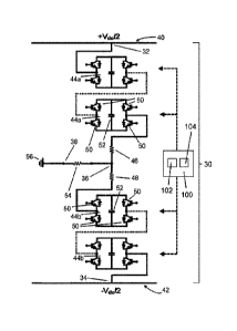
A control circuit 30 according to a first
embodiment of the invention is shown in Figure 2.
The first control circuit 30 comprises
first and second primary terminals 32,34, a secondary
terminal 36 and an auxiliary terminal 38.
In use, the first primary terminal 32 is
connected to a first DC transmission line 40 that is at
a positive voltage, +VDc/2, while the second primary
terminal 34 is connected to a second DC transmission
line 42 that is at a negative voltage, -VDc/2.
The first control circuit 30 further
includes a plurality of modules 44a,44b that are
CA 02865447 2014-003-25
WO 2013/127461 14
PCT/EP2012/053571
connected in series with first and second primary
resistors 46,48 between the first and second primary
terminals 32,34 to define a current transmission path.
Each module 44a,44b includes two pairs of
switching elements 50 connected in parallel with an
energy storage device in the form of a capacitor 52.
The switching elements 50 and the capacitor 52 are
connected in a full-bridge arrangement which defines a
4-quadrant bipolar module 44a,44b that can provide a
negative, zero or positive voltage and can conduct
current in two directions.
The plurality of modules 44a,44b is divided
into a plurality of first modules 44a and a plurality
of second modules 44b. The plurality of first modules
44a is connected in series with the first primary
resistor 46 between the first primary terminal 32 and
the secondary terminal 36 to define a first current
transmission path portion, while the plurality of
second modules 44b is connected in series with the
second primary resistor 48 between the second primary
terminal 34 and the secondary terminal 36 to define a
second current transmission path portion.
The secondary terminal 36 is connected in
series between the first and second primary terminals
32,34 to define a mid-point of the current transmission
path that separates the first and second current
transmission path portions.
In other embodiments of the invention, it
is envisaged that each primary resistor 46,48 may be
replaced by a plurality of primary resistors. It is
further envisaged that, in such embodiments, the
CA 02865447 2014-003-25
WO 2013/127461 15
PCT/EP2012/053571
modules and primary resistors in each of the first and
second current transmission portion may be re-arranged
to define different series-connected arrangements. For
example, the modules and primary resistors of each
current transmission path portion may be arranged to
define an alternating sequence of series-connected
modules and primary resistors.
The first control circuit 30 further
includes an auxiliary resistor 54 connected in series
between the secondary and auxiliary terminals 36,38.
The auxiliary resistor 54 is preferably
sized to have the same resistance value as each of the
first and second primary resistors 46,48, but may be
sized to have a higher resistance than each of the
first and second primary resistors 46,48.
In other embodiments of the invention, it
is envisaged that the auxiliary resistor 54 may be
replaced by a plurality of auxiliary resistors.
In use, the auxiliary terminal 38 is
connected to ground 56.
It is envisaged that, in other embodiments
of the invention, each of the primary and auxiliary
resistors 46,48,54 may be replaced by another type of
energy conversion element that is capable of
dissipating electrical energy.
The capacitor 52 of each module 44a,44b may
be selectively removed from the current transmission
path, i.e. switched in or out of circuit with the
corresponding primary resistor 46,48, by changing the
state of the switching elements 50. This allows the
CA 02865447 2014-003-25
WO 2013/127461 16
PCT/EP2012/053571
current in the first control circuit 30 to selectively
flow through or bypass each capacitor 52.
The capacitor 52 of each module 44a,44b is
removed from the current transmission path, i.e.
switched out of circuit with the corresponding primary
resistor 46,48, when the pairs of switching elements 50
are configured to form a short circuit in the module
44a,44b. This causes the current in the first control
circuit 30 to pass through the short circuit and bypass
the capacitor 52. Such a configuration allows the
module 44a,44b to provide a zero voltage.
The capacitor 52 of each module 44a,44b is
returned to the current transmission path, i.e.
switched back into circuit with the corresponding
primary resistor 46,48, when the pairs of switching
elements 50 are configured to allow the current in the
first control circuit 30 to flow into and out of the
capacitor 52. The capacitor 52 is then able to charge
or discharge its stored energy and provide a voltage.
The bidirectional nature of the 4-quadrant bipolar
module 44a,44b means that the capacitor 52 may be
inserted into the 4-quadrant bipolar module 44a,44b in
either forward or reverse directions so as to provide a
positive or negative voltage.
Each module 44a,44b may be configured to
selectively block current from flowing therethrough by
changing the state of the switching elements 50 to stop
conducting current. When current is blocked from
flowing through a module 44a,44b, its capacitor 52 is
prevented from charging or discharging its stored
energy and thereby remains at a constant voltage level.
CA 02865447 2014-003-25
WO 2013/127461 17
PCT/EP2012/053571
It is envisaged that the two pairs of
switching elements 50 of each module 44a,44b may be
replaced by other configurations that are capable of
selectively removing a corresponding energy storage
device, e.g. a capacitor, from the current transmission
path and blocking current from flowing through the
module 44a,44b in the aforementioned manner.
Each switching element 50 includes an
insulated gate bipolar transistor (IGBT) connected in
parallel with an anti-parallel diode. In other
embodiments of the invention, each switching element 50
may include a gate turn-off thyristor, a field effect
transistor, an injection enhanced gate transistor or an
integrated gate commutated thyristor, or other force-
commutated or self-commutated semiconductor switches.
In still further embodiments of the
invention, each capacitor 52 may be replaced by another
energy storage device such as a battery, or a fuel
cell, or any device that is capable of storing and
releasing electrical energy to provide a voltage.
The plurality of first modules 44a and the
plurality of second modules 44b each define a chain-
link converter. It is possible to build up a combined
voltage across each chain-link converter, which is
higher than the voltage available from each of its
individual modules 44a,44b, via the insertion of the
capacitors 52 of multiple modules 44a,44b, each
providing its own voltage, into each chain-link
converter.
In this manner switching of the switching
elements 50 of each 4-quadrant bipolar module 44a,44b
CA 02865447 2014-003-25
WO 2013/127461 18
PCT/EP2012/053571
causes each chain-link converter to provide a stepped
variable voltage source, which permits the generation
of a voltage waveform across each chain-link converter
using a step-wise approximation.
The first control circuit 30 further
includes a control unit 100 having first and second
controllers 102,104. The first controller 102 switches
the switching elements 50 in each module 44a,44b to
selectively remove its capacitor 52 from or insert its
capacitor 52 into the current transmission path. The
second controller 104 selectively switches the
switching element 50 in each module 44a,44b to
selectively block current from flowing through each
module 44a,44b.
The operation of the first control circuit
30 shown in Figure 2 within a DC power transmission
scheme is described below with reference to Figures 2
to 7.
The first and second DC transmission lines
40,42 interconnect first and second power converters
(not shown) that are themselves connected to respective
phases of corresponding first and second AC networks
(not shown). Power is transmitted from the first AC
network to the second AC network via the corresponding
power converters and the first and second DC
transmission lines 40,42.
During normal operation of the DC
transmission scheme, the first control circuit 30
adopts a standby configuration in which the capacitor
52 of each module 44a,44b is inserted into the current
CA 02865447 2014-003-25
WO 2013/127461 19
PCT/EP2012/053571
transmission path, i.e. switched into circuit with the
corresponding primary resistor 46,48.
The total voltage across the modules
44a,44b is approximately equal to VDcr which is the DC
transmission scheme voltage across the DC transmission
lines 40,42. In this configuration there is zero or
minimal current flowing through the current
transmission path, i.e. through the modules 44a,44b and
the primary resistors 46,48.
In the event that the second power
converter is unable to receive the transmitted power as
a result of, for example, a fault in the second AC
network, the first AC network must temporarily continue
transmitting power into the DC transmission lines 40,42
until the power transfer can be reduced to zero, which
is typically 1-2 seconds for a wind generation plant.
In order to allow the first AC network to
continue transmitting power into the DC transmission
lines 40,42 via the first power converter, the control
unit 100 selectively removes one or more capacitors 52
of the first and/or second modules 44a,44b from the
current transmission path. This results in the
generation of a voltage waveform across the current
transmission path, which adds or subtracts finite
voltage steps to the voltage Vdc across the DC
transmission lines 40,42. This in turn imposes a
voltage waveform across the primary resistors 46,48 and
thereby causes a current waveform to flow from the DC
transmission lines 40,42 through the current
transmission path and the primary resistors 46,48. As
such, energy may be transferred from the DC
CA 02865447 2014-003-25
WO 2013/127461 20
PCT/EP2012/053571
transmission lines 40,42 and dissipated via the primary
resistors 46,48.
The current waveform may be modulated to
form different shapes by including one or more current
components having different current characteristics so
as to vary characteristics of energy removed from the
DC transmission lines 40,42.
During modulation of the current waveform,
the control unit 100 may selectively insert each
capacitor 52 in either forward or reverse directions to
offset any increase in energy level with a
corresponding decrease in energy level, and vice versa,
over a single duty cycle of the first control circuit
30. This allows the first control circuit 30 to
maintain a zero net change in energy level of each
chain-link converter and thereby maintain the average
energy level of each chain-link converter at a constant
value, whilst the first control circuit 30 is
controlled to remove excess energy from the DC
transmission lines 40,42.
Following the removal of excess energy from
the DC transmission lines 40,42 through power
dissipation via the primary resistors 46,48, the first
controller 102 switches the switching elements 50 of
the modules 44a,44b to switch each capacitor 52 back
into circuit with the corresponding primary resistor
46,48. Such a configuration turns off the current
flowing in the first control circuit 30, which allows
the DC transmission scheme to revert to normal
operation.
CA 02865447 2014-003-25
WO 2013/127461 21
PCT/EP2012/053571
During normal operation of the first
control circuit 30, the maximum voltage across each of
the first and second current transmission path portions
is equal to half of the DC transmission scheme voltage
Vdc, i.e. 0.5 Vdc, while the maximum current flowing
through each of the first and second current
transmission path portions is equal to half of the DC
transmission scheme voltage Vdc divided by the
resistance of the corresponding primary resistor 46,48
when all of the capacitors 52 are removed from the
respective current transmission path portion. Each
module 44a,44b and primary resistor 46,48 is therefore
rated to be compatible with these maximum voltage and
current levels arising during normal operation of the
first control circuit 30.
A fault or other abnormal operating
condition in the DC transmission scheme may lead to a
DC pole-to-ground fault 58 occurring between one of the
DC transmission lines 40,42 and ground 56, i.e. a short
circuit between one of the DC transmission lines 40,42
and ground 56 that bypasses the corresponding current
transmission path portion.
For the purposes of this specification, the
following fault operation of the first control circuit
30 during the DC pole-to-ground fault 58 is described
with reference to a short circuit between the second DC
transmission line 42 and ground 56 that bypasses the
second current transmission path portion, as shown in
Figure 3.
In the event of the DC pole-to-ground fault
58, the resulting short-circuit between the second DC
CA 02865447 2014-003-25
WO 2013/127461 22
PCT/EP2012/053571
transmission line 42 and ground 56 causes the voltage
difference between the second DC transmission line 42
and ground 56 to collapse to zero voltage.
As soon as the DC pole-to-ground fault 58
is detected, the control unit 100 enters a fault
protection mode, as shown in Figure 4.
In the fault protection mode, the control
unit 100 selectively removes the capacitors 52 of the
first and second modules 44a,44b from the current
transmission path. The removed capacitors 52 therefore
cannot conduct current and therefore cannot be charged
or discharged. Thus, the voltage level of each
capacitor 52 remains the same whilst it is removed from
the current transmission path, and is thereby protected
from damage due to overvoltage.
Removal of the capacitors 52 of the first
modules 44a from the current transmission path results
in the DC transmission scheme voltage Vdc being imposed
across the first primary resistor 46 and the auxiliary
resistor 54. Since the auxiliary resistor 54 has the
same resistance as the first primary resistor 46, the
voltage drop across the first primary resistor 46 is
equal to 0.5 Vdc. The maximum current flowing through
the first primary resistor 46 during the DC pole-to-
ground fault 58 is therefore equal to 0.5 Vdc divided
by the resistance of the first primary resistor 46,
which is equal to the maximum current level flowing
through the first primary resistor 46 during normal
operation of the first control circuit 30. Thus, the
first modules 44a and the first primary resistor 46 are
protected from damage due to overcurrent.
CA 02865447 2014-003-25
WO 2013/127461 23
PCT/EP2012/053571
Optionally, in the fault protection mode,
the control unit 100 may selectively switch the second
modules 44b to block current from flowing therethrough,
instead of selectively removing the capacitors 52 of
the second modules 44b from the current transmission
path.
Meanwhile the first DC transmission line 40
is overcharged to Vdc as a result of its exposure to
the DC transmission scheme voltage Vdc during the DC
pole-to-ground fault 58.
The first control circuit 30 is therefore
operable in the fault protection mode to protect the
components of the first control circuit 30 from
overvoltage and overcurrent situations during the DC
pole-to-ground fault 58, until the DC pole-to-ground
fault 58 has been cleared.
After the DC pole-to-ground fault 58 has
been cleared, the first control circuit 30 enters a
network discharging mode, as shown in Figure 5.
In the network discharging mode, the
control unit 100 selectively removes the capacitors 52
of the first modules 44a from the current transmission
path. This causes a current waveform 60 to flow from
the first DC transmission line 40 to ground 56 via the
first current transmission path portion. This enables
excess energy to be drawn from the overcharged, first
DC transmission line 40 and dissipated via the first
primary resistor 46 and the auxiliary resistor 54.
At the same time, the control unit 100
selectively switches the second modules 44b to block
current from flowing therethrough, so as to prevent
CA 02865447 2014-003-25
WO 2013/127461 24
PCT/EP2012/053571
energy from being drawn from the second DC transmission
line 42 during the network discharging mode.
Optionally, the control unit 100 may
selectively insert one or more capacitors 52 of the
first modules 44a into the current transmission path to
produce a negative voltage to speed up the discharging
process, or to produce a varying voltage to control the
rate of discharge of the first DC transmission line 40.
Once the first DC transmission line 40 is
discharged back to its normal operating voltage of
+Vdc/2, the first control circuit 30 exits the network
discharging mode and selectively inserts all the
capacitors 52 of the first and second modules 44a,44b
into the current transmission path. This returns the
first control circuit 30 to its standby configuration,
and enables the DC transmission scheme and the first
control circuit 30 to resume normal operation.
It will be appreciated that the above-
described fault operation of the first control circuit
30 during the DC pole-to-ground fault 58 is equally
applicable to a short circuit occurring between the
first DC transmission line 40 and ground 56 that
bypasses the first current transmission path portion.
The inclusion of the auxiliary resistor 54
in the first control circuit 30 therefore permits
control over the maximum voltage and current levels
seen by the components of the first control circuit 30
so as to be the same during normal and fault operation
of the first control circuit 30. This therefore
obviates the need to increase the voltage and current
ratings of the components of the first control circuit
CA 02865447 2014-003-25
WO 2013/127461 25
PCT/EP2012/053571
30, and thereby minimises the overall size and cost of
the first control circuit 30.
In addition, the modules 44, first and
second primary resistors 46,48 and control unit 100 are
used in both normal and fault operations of the first
control circuit 30. This thereby removes the need for
additional equipment to protect the components of the
first control circuit 30 from overvoltage and
overcurrent situations, and thereby minimises the size
and complexity of the first control circuit 30.
The first control circuit 30 is therefore
not only capable of regulating energy levels in the DC
transmission lines 40,42, but is also capable of
protecting its components in a cost-efficient manner.
It is envisaged that, in embodiments of the
invention, the control unit 100 may selectively remove
one or more capacitors 52 from the current transmission
path during normal operation of the control circuit to
charge one or more other capacitors 52, which are
inserted into the current transmission path, through
absorption of energy from the DC transmission lines
40,42 to offset any operating losses of each module
44a,44b and thereby maintain the average energy level
of each module 44a,44b at a constant value.
A fault or other abnormal operating
condition in the DC transmission scheme may also lead
to a DC pole-to-pole fault 62 occurring between the DC
transmission lines 40,42, i.e. a short circuit between
the DC transmission lines 40,42 that bypasses the first
control circuit 30.
CA 02865447 2014-003-25
WO 2013/127461 26
PCT/EP2012/053571
In the event of the DC pole-to-pole fault
62, the resulting short-circuit between the DC
transmission lines 40,42 causes the voltage difference
between the DC transmission lines 40,42 to collapse to
zero voltage, as shown in Figure 6.
As soon as the DC pole-to-pole fault 62 is
detected, the control unit 100 selectively removes the
capacitors 52 of the first and second modules 44a,44b
from the current transmission path, as shown in Figure
7. The removed capacitors 52 cannot conduct current and
therefore cannot be charged or discharged. Thus, the
voltage level of each capacitor 52 remains the same
whilst it is removed from the current transmission
path, and is thereby protected from damage due to
overvoltage.
Optionally, as soon as the DC pole-to-pole
fault 62 is detected, the control unit 100 may
selectively switch the first and second modules 44a,44b
to block current from flowing therethrough, instead of
selectively removing the capacitors 52 of the first and
second modules 44a,44b from the current transmission
path. Thus, current is prevented from flowing through
each module 44a,44b through turn-off of the IGBTs and
reverse-biasing of the anti-parallel diodes resulting
from the sum of the voltages of the capacitors 52
exceeding the zero voltage across the DC transmission
lines 40,42.
After the DC pole-to-pole fault 62 has been
cleared, a rectifier station (not shown) is used to
charge the DC transmission cables back to their normal
operating voltages. Once the DC transmission lines
CA 02865447 2014-003-25
WO 2013/127461 27
PCT/EP2012/053571
40,42 are charged back to their respective normal
operating voltages, the first control circuit 30
selectively inserts all the capacitors 52 of the
modules 44a,44b into the current transmission path.
This returns the first control circuit 30 to its
standby configuration, and enables the DC transmission
scheme and first control circuit 30 to resume normal
operation.
A control circuit 70 according to a second
embodiment of the invention is shown in Figure 8. The
second control circuit 70 is similar in structure and
operation to the first control circuit 30 shown in
Figure 2 and like features share the same reference
numerals.
The second control circuit 70 differs from
the first control circuit 30 in that each module
72a,72b of the second control circuit 70 includes first
and second sets of series-connected current flow
control elements 74,76 that are connected in parallel
with a capacitor 78 in a full-bridge arrangement to
define a 2-quadrant rationalised bipolar module 72a,72b
that can provide zero, positive or negative voltage
while conducting current in a single direction.
Each set of the series-connected current
flow control elements 74,76 includes a switching
element 80, which in the embodiment shown is an IGBT
connected in parallel with an anti-parallel diode, to
selectively direct current through the capacitor 78,
and a secondary passive current check element 82, which
is in the form of a diode to limit current flow through
the module 72a,72b to a single direction.
CA 02865447 2014-08-25
WO 2013/127461 28
PCT/EP2012/053571
The configuration of each module 72a,72b in
the second control circuit 70 reduces the overall
number of components, and therefore reduces the size
and cost of the second control circuit 70 in comparison
to the first control circuit 30.