Note: Descriptions are shown in the official language in which they were submitted.
CA 02865641 2014-08-26
WO 2013/162744
PCT/US2013/031467
DEVICES FOR OPTICALLY DETERMINING A CHARACTERISTIC OF A SUBSTANCE
BACKGROUND
[0001] The
present invention generally relates to systems and
methods of optical computing and, more specifically, to systems and methods of
determining a particular characteristic of a substance using two or more
integrated computational elements.
[0002] Spectroscopic techniques for measuring
various
characteristics of materials are well known and are routinely used under
laboratory conditions. In some cases, these spectroscopic techniques can be
carried out without using an involved sample preparation. It is more common,
however, to carry out various sample preparation steps before conducting the
analysis. Reasons for conducting sample preparation steps can include, for
example, removing interfering background materials from the analyte of
interest, converting the analyte of interest into a chemical form that can be
better detected by the chosen spectroscopic technique, and adding standards to
improve the accuracy of quantitative measurements. Thus, there is usually a
delay in obtaining an analysis due to sample preparation time, even
discounting
the transit time of transporting the sample to a laboratory.
[0003]
Although spectroscopic techniques can, at least in principle,
be conducted at a job site or in a process, the foregoing concerns regarding
sample preparation times can still apply.
Furthermore, the transitioning of
spectroscopic instruments from a laboratory into a field or process
environment
can be expensive and complex. Reasons for these issues can include, for
example, the need to overcome inconsistent temperature, humidity, and
vibration encountered during field or process use.
Furthermore, sample
preparation, when required, can be difficult under field analysis conditions.
The
difficulty of performing sample preparation in the field can be especially
problematic in the presence of interfering materials, which can further
complicate conventional spectroscopic analyses.
Quantitative spectroscopic
measurements can be particularly challenging in both field and laboratory
settings due to the need for precision and accuracy in sample preparation and
spectral interpretation.
1
CA 02865641 2014-08-26
WO 2013/162744
PCT/US2013/031467
SUMMARY OF THE INVENTION
[0004]
The present invention generally relates to systems and
methods of optical computing and, more specifically, to systems and methods of
determining a particular characteristic of a substance using two or more
integrated computational elements.
[0005]
In some embodiments of the disclosure, a device is disclosed
that may include an electromagnetic radiation source configured to optically
interact with a sample having a characteristic of interest, and a first
integrated
computational element arranged within a primary channel and configured to
optically interact with the electromagnetic radiation source and produce a
first
modified electromagnetic radiation. The device may also include a second
integrated computational element arranged within a reference channel and
configured to optically interact with the electromagnetic radiation source and
produce a second modified electromagnetic radiation, and a first detector
arranged to receive the first and second modified electromagnetic radiations
from the first and second integrated computational elements, respectively, and
generate an output signal corresponding to the characteristic of the sample.
[0006]
In some embodiments of the disclosure, a method of
determining a characteristic of a sample is disclosed. The method may include
optically interacting an electromagnetic radiation source with the sample and
a
first integrated computational element arranged within a primary channel and a
second integrated computational element arranged within a reference channel.
The method may also include producing first and second modified
electromagnetic radiations from the first and second integrated computational
elements, respectively, and receiving the first and second modified
electromagnetic radiations with a first detector. The method may further
include
generating an output signal with the first detector, the output signal
corresponding to the characteristic of the sample.
[0007] In some
embodiments of the disclosure, another device is
disclosed and may include an electromagnetic radiation source configured to
optically interact with a sample having a characteristic of interest, and a
first
integrated computational element arranged within a primary channel and
configured to optically interact with the electromagnetic radiation source and
produce a first modified electromagnetic radiation. The device may also
include
2
CA 02865641 2014-08-26
WO 2013/162744
PCT/US2013/031467
a second integrated computational element arranged within a second channel
and configured to optically interact with the electromagnetic radiation source
and
produce a second modified electromagnetic radiation, and a first detector
arranged to receive the first modified electromagnetic radiation and generate
a
first output signal. The device may further include a second detector arranged
to receive the second modified electromagnetic radiation and generate a second
output signal, and a signal processor configured to receive and
computationally
combine the first and second output signals to determine the characteristic of
interest of the sample.
[0008] In some
embodiments of the disclosure, another method of
determining a characteristic of a sample is disclosed. The method may include
optically interacting an electromagnetic radiation source with the sample and
a
first integrated computational element arranged within a primary channel and a
second integrated computational element arranged within a reference channel,
and producing first and second modified electromagnetic radiations from the
first
and second integrated computational elements, respectively. The method may
also include receiving the first modified electromagnetic radiation with a
first
detector, and receiving the second modified electromagnetic radiation with a
second detector. The method may further include generating a first output
signal with the first detector and a second output signal with the second
detector, and computationally combining the first and second output with a
signal processor to determine the characteristic of interest of the sample.
[0009]
The features and advantages of the present invention will be
readily apparent to one having ordinary skill in the art upon a reading of the
description of the preferred embodiments that follows.
BRIEF DESCRIPTION OF THE DRAWINGS
[0010]
The following figures are included to illustrate certain aspects
of the present invention, and should not be viewed as exclusive embodiments.
The subject matter disclosed is capable of considerable modification,
alteration,
and equivalents in form and function, as will occur to one having ordinary
skill in
the art and having the benefit of this disclosure.
[0011]
FIG. 1 illustrates an exemplary integrated computation
element, according to one or more embodiments.
3
CA 02865641 2014-08-26
WO 2013/162744
PCT/US2013/031467
[0012]
FIG. 2a illustrates a block diagram non-mechanistically
illustrating how an optical computing device distinguishes electromagnetic
radiation related to a characteristic of interest from other electromagnetic
radiation, according to one or more embodiments.
[0013] FIG. 2b
illustrates another block diagram non-mechanistically
illustrating how an optical computing device distinguishes electromagnetic
radiation related to a characteristic of interest from other electromagnetic
radiation, according to one or more embodiments.
[0014]
FIG. 3a illustrates an exemplary optical computing device,
according to one or more embodiments.
[0015]
FIG. 3b illustrates another exemplary optical computing
device, according to one or more embodiments.
[0016]
FIG. 4 illustrates a graph indicating the advantages of
arranging integrated computational elements in both the primary and reference
channels, according to one or more embodiments.
[0017]
FIG. 5 illustrates another exemplary optical computing
device, according to one or more embodiments.
[0018]
FIG. 6 illustrates another exemplary optical computing
device, according to one or more embodiments.
[0019] FIG. 7
illustrates another exemplary optical computing
device, according to one or more embodiments.
[0020]
FIGS. 8 and 9 illustrate variations of the optical computing
device of FIG. 7, according to one or more embodiments.
[0021]
FIG. 10 illustrates another exemplary optical computing
device, according to one or more embodiments.
[0022]
FIG. 11 illustrates another exemplary optical computing
device, according to one or more embodiments.
DETAILED DESCRIPTION
[0023] The
present invention generally relates to systems and
methods of optical computing and, more specifically, to systems and methods of
determining a particular characteristic of a substance using two or more
integrated computational elements.
[0024]
Embodiments described herein include various configurations
of optical computing devices, also commonly referred to as opticoanalytical
4
CA 02865641 2014-08-26
WO 2013/162744
PCT/US2013/031467
devices. The various embodiments of the disclosed optical computing devices
may be suitable for use in the oil and gas industry. For example, embodiments
disclosed herein provide systems and/or devices capable of providing a
relatively
low cost, rugged, and accurate system for monitoring petroleum quality for the
purpose of optimizing decision making at a well site and efficient management
of
hydrocarbon production. Embodiments disclosed herein may also be useful in
determining concentrations of various analytes of interest in hydrocarbons
present within a wellbore. Embodiments disclosed herein may also be useful in
determining concentrations of various analytes of interest in other fluids,
such as
water, important in the oil and gas industry. It will be appreciated, however,
that the various disclosed systems and devices are equally applicable to other
technology fields including, but not limited to, the food and drug industry,
industrial applications, mining industries, or any field where it may be
advantageous to determine in real-time the concentrations of a specific
character or analyte of interest of a compound or material.
[0025]
As used herein, the term "fluid" refers to any substance that
is capable of flowing, including particulate solids, liquids, gases, slurries,
emulsions, powders, muds, glasses, combinations thereof, and the like. In
some embodiments, the fluid can be an aqueous fluid, including water or the
like. In some embodiments, the fluid can be a non-aqueous fluid, including
organic compounds, more specifically, hydrocarbons, oil, a refined component
of
oil, petrochemical products, and the like. In some embodiments, the fluid can
be a treatment fluid or a formation fluid. Fluids can include various flowable
mixtures of solids, liquid and/or gases. Illustrative gases that can be
considered
fluids according to the present embodiments include, for example, air,
nitrogen,
carbon dioxide, argon, helium, hydrogen disulfide, mercaptan, thiophene,
methane, ethane, butane, and other hydrocarbon gases, and/or the like.
[0026]
As used herein, the term "characteristic" refers to a chemical,
mechanical, or physical property of a substance. A characteristic of a
substance
may include a quantitative value of one or more chemical components therein.
Such chemical components may be referred to as "analytes." Illustrative
characteristics of a substance that can be monitored with the optical
computing
devices disclosed herein can include, for example, chemical composition
(identity
and concentration, in total or of individual components), impurity content,
pH,
5
CA 02865641 2014-08-26
WO 2013/162744
PCT/US2013/031467
viscosity, density, ionic strength, total dissolved solids, salt content,
porosity,
opacity, bacteria content, combinations thereof, and the like.
[0027]
As used herein, the term "electromagnetic radiation" refers
to radio waves, microwave radiation, infrared and near-infrared radiation,
visible
light, ultraviolet light, X-ray radiation and gamma ray radiation.
[0028]
As used herein, the term "optical computing device" refers to
an optical device that is configured to receive an input of electromagnetic
radiation from a substance or sample of the substance and produce an output of
electromagnetic radiation from a processing element. The processing element
may be, for example, an integrated computational element.
The
electromagnetic radiation emanating from the processing element is changed in
some way so as to be readable by a detector, such that an output of the
detector can be correlated to at least one characteristic of the substance.
The
output of electromagnetic radiation from the processing element can be
reflected
electromagnetic radiation, transmitted electromagnetic radiation, and/or
dispersed electromagnetic radiation. As will be appreciated by those skilled
in
the art, whether reflected or transmitted electromagnetic radiation is
analyzed
by the detector will be a matter of routine experimental design. In addition,
emission and/or scattering of the substance, for example via fluorescence,
luminescence, radiation and re-radiation, Raman scattering, and/or Raleigh
scattering can also be monitored by the optical computing devices.
[0029]
As used herein, the term "optically interact" or variations
thereof refers to the reflection, transmission, scattering, diffraction,
radiating,
re-radiating, or absorption of electromagnetic radiation either on, through,
or
from one or more processing elements, such as integrated computational
elements. Accordingly, optically interacted light refers to light that has
been
reflected, transmitted, scattered, diffracted, or absorbed by, emitted,
radiated,
or re-radiated, for example, using the integrated computational elements, but
may also apply to interaction with a sample substance.
[0030] As used
herein, the term "sample," or variations thereof,
refers to at least a portion of a substance of interest to be tested or
otherwise
evaluated using the optical computing devices described herein. The sample
includes the characteristic of interest, as defined above, and may be any
fluid, as
defined herein, or otherwise any solid substance or material such as, but not
limited to, rock formations, concrete, other solid surfaces, etc.
6
CA 02865641 2017-01-23
[0031] At the very least, the exemplary optical computing devices
disclosed
herein will each include an electromagnetic radiation source, at least two
processing elements
(e.g., integrated computational elements), and at least one detector arranged
to receive
optically interacted light from the at least two processing elements. As
disclosed below,
however, in one or more embodiments, the electromagnetic radiation source may
be omitted
and instead the electromagnetic radiation may be derived from the substance
itself or a
sample of the substance. In some embodiments, the exemplary optical computing
devices
may be specifically configured for detecting, analyzing, and quantitatively
measuring a
particular characteristic or analyte of interest of a given sample or
substance. In other
embodiments, the exemplary optical computing devices may be general purpose
optical
devices, with post-acquisition processing (e.g., through computer means) being
used to
specifically detect the characteristic of the sample.
[0032] In some embodiments, suitable structural components for the
exemplary
optical computing devices disclosed herein are described in commonly owned U
.S. Pat. Nos.
6,198,531; 6,529,276; 7,123,844; 7,834,999; 7,711,605, 7,920,258, and
8,049,881 and U .S.
Pat. App. Serial Nos. 12/094,460 (U .S. Pat. App. Pub. No. 2009/0219538); and
12/094,465
(U .S. Pat. App. Pub. No. 2009/0219539). As will be appreciated, variations of
the structural
components of the optical computing devices described in the above-referenced
patents and
patent applications may be suitable, without departing from the scope of the
disclosure, and
therefore should not be considered limiting to the various embodiments
disclosed herein.
[0033] The optical computing devices described in the foregoing patents
and
patent applications combine the advantage of the power, precision and accuracy
associated
with laboratory spectrometers, while being extremely rugged and suitable for
field use.
Furthermore, the optical computing devices can perform calculations (analyses)
in real-time
or near real-time without the need for sample processing . In this regard, the
optical
computing devices can be specifically configured to detect and analyze
particular
characteristics and/or analytes of interest. As a result, interfering signals
are discriminated
from those of interest in a sample by appropriate configuration of the optical
computing
7
CA 02865641 2014-08-26
WO 2013/162744
PCT/US2013/031467
devices, such that the optical computing devices provide a rapid response
regarding the characteristics of the sample as based on the detected output.
In
some embodiments, the detected output can be converted into a voltage that is
distinctive of the magnitude of the characteristic being monitored in the
sample.
The foregoing advantages and others make the optical computing devices, and
their variations generally described below, particularly well suited for field
and
downhole use.
[0034]
The exemplary optical computing devices described herein
can be configured to detect not only the composition and concentrations of a
material or mixture of materials, but they also can be configured to determine
physical properties and other characteristics of the material as well, based
on
their analysis of the electromagnetic radiation received from the sample. For
example, the optical computing devices can be configured to determine the
concentration of an analyte and correlate the determined concentration to a
characteristic of a substance by using suitable processing means. As will be
appreciated, the optical computing devices may be configured to detect as many
characteristics or analytes as desired in a given sample. All that is required
to
accomplish the monitoring of multiple characteristics or analytes is the
incorporation of suitable processing and detection means within the optical
computing device for each characteristic or analyte. In some embodiments, the
properties of a substance can be a combination of the properties of the
analytes
therein (e.g., a linear, non-linear, logarithmic, and/or exponential
combination).
Accordingly, the more characteristics and analytes that are detected and
analyzed using the exemplary optical computing devices, the more accurately
the properties of the given sample can be determined.
[0035] Fundamentally, optical computing devices
utilize
electromagnetic radiation to perform calculations, as opposed to the hardwired
circuits of conventional electronic processors. When electromagnetic radiation
interacts with a substance, unique physical and chemical information about the
substance is encoded in the electromagnetic radiation that is reflected from,
transmitted through, or radiated from the sample. This information is often
referred to as the substance's spectral "fingerprint." The exemplary optical
computing devices disclosed herein are capable of extracting the information
of
the spectral fingerprint of multiple characteristics or analytes within a
substance
and converting that information into a detectable output regarding the overall
8
CA 02865641 2014-08-26
WO 2013/162744
PCT/US2013/031467
properties of a sample. That is, through suitable configurations of the
exemplary
optical computing devices, electromagnetic radiation associated with
characteristics or analytes of interest in a substance can be distinguished
from
electromagnetic radiation associated with all other components of a sample in
order to estimate the sample's properties in real-time or near real-time.
[0036]
The processing elements used in the exemplary optical
computing devices described herein may be characterized as integrated
computational elements (ICE).
The ICE are capable of distinguishing
electromagnetic radiation related to the characteristic or analyte of interest
from
electromagnetic radiation related to other components of a sample substance.
Referring to FIG. 1, illustrated is an exemplary ICE 100 suitable for use in
the
various optical computing devices described herein, according to one or more
embodiments. As illustrated, the ICE 100 may include a plurality of
alternating
layers 102 and 104, such as silicon (Si) and 5i02 (quartz), respectively. In
general, these layers consist of materials whose index of refraction is high
and
low, respectively. Other examples might include niobia and niobium, germanium
and germania, MgF, SiO, and other high and low index materials as known in the
art. The layers 102, 104 may be strategically deposited on an optical
substrate
106. In some embodiments, the optical substrate 106 is BK-7 optical glass. In
other embodiments, the optical substrate 106 may be other types of optical
substrates, such as quartz, sapphire, silicon, germanium, zinc selenide, zinc
sulfide, or various plastics such as polycarbonate, polymethalmethacrylate
(PM MA), polyvinylchloride (PVC), diamond, ceramics, etc., as known in the
art.
[0037]
At the opposite end (e.g., opposite the optical substrate
106), the ICE 100 may include a layer 108 that is generally exposed to the
environment of the device or installation. The number of layers 102, 104 and
the thickness of each layer 102, 104 are determined from the spectral
attributes
acquired from a spectroscopic analysis of a characteristic of the sample
substance using a conventional spectroscopic instrument. The spectrum of
interest of a given characteristic of a sample typically includes any number
of
different wavelengths. It should be understood that the exemplary ICE 100 in
FIG. 1 does not in fact represent any particular characteristic of a given
sample,
but is provided for purposes of illustration only. Consequently, the number of
layers 102, 104 and their relative thicknesses, as shown in FIG. 1, bear no
correlation to any particular characteristic of a given sample. Nor are the
layers
9
CA 02865641 2016-05-11
102, 104 and their relative thicknesses, as shown in FIG. 1, bear no
correlation to any
particular characteristic of a given sample. Nor are the layers 102, 104 and
their relative -
thicknesses necessarily drawn to scale, and therefore should not be considered
limiting of the
present disclosure. Moreover, those skilled in the art will readily recognize
that the materials
that make up each layer 102, 104 (i.e., Si and Si02) may vary, depending on
the application,
cost of materials, and/or applicability of the material to the sample
substance. For example,
the layers 102, 104 may be made of, but are not limited to, silicon,
germanium, water,
combinations thereof, or other materials of interest.
[0038] In some
embodiments, the material of each layer 102, 104 can be doped or
two or more materials can be combined in a manner to achieve the desired
optical
characteristic. In addition to solids, the exemplary ICE 100 may also contain
liquids and/or
gases, optionally in combination with solids, in order to produce a desired
optical
characteristic. In the case of gases and liquids, the ICE 100 can contain a
corresponding
vessel (not shown) which houses the gases or liquids. Exemplary variations of
the ICE 100
may also include holographic optical elements, gratings, piezoelectric, light
pipe, digital light
pipe (DLP), and/or acousto-optic elements, for example, that can create
transmission,
reflection, and/or absorptive properties of interest.
[0039] multiple
layers 102, 104 exhibit different refractive indices. By properly
selecting the materials of the layers 102, 104 and their relative spacing, the
exemplary ICE
100 may be configured to selectively pass/reflect/refract predetermined
fractions of light (i.e.,
electromagnetic radiation) at different wavelengths. Each wavelength is given
a
predetermined weighting or loading factor. The thicknesses and spacing of the
layers 102,
104 may be determined using a variety of approximation methods from the
spectrograph of
the character or analyte of interest. These methods may include inverse
Fourier transform
(IFT) of the optical transmission spectrum and structuring the ICE 100 as the
physical
representation of the WT. The approximations convert the IFT into a structure
based on
known materials with constant refractive indices. Further information
regarding the structures
and design of exemplary integrated computational elements (also referred to as
multivariate
optical elements) is provided in Applied Optics, Vol. 35, pp. 5484-5492 (1996)
and Vol. 129,
pp. 2876-2893.
[0040] The
weightings that the layers 102, 104 of the ICE 100 apply at each
wavelength are set to the regression weightings described with respect
CA 02865641 2016-05-11
to a known equation, or data, or spectral signature. Briefly, the ICE 100 may
be configured to
perform the dot product of the input light beam into the ICE 100 and a desired
loaded
regression vector represented by each layer 102, 104 for each wavelength . As
a result, the
output light intensity of the ICE 100 is related to the characteristic or
analyte of interest.
Further details regarding how the exemplary ICE 100 is able to distinguish and
process
electromagnetic radiation related to the characteristic or analyte of interest
are described in
U.S. Patent Nos. 6,198,531; 6,529,276; and 7,920,258.
[0041] Referring now to FIG. 2a, illustrated is a block diagram that non-
mechanistically illustrates how an optical computing device 200 is able to
distinguish
electromagnetic radiation related to a characteristic of a sample 202 from
other
electromagnetic radiation . As shown in FIG . 2a, an electromagnetic radiation
source 201
emits or otherwise generates electromagnetic radiation 204. The
electromagnetic radiation
source 201 may be any device capable of emitting or generating electromagnetic
radiation, as
defined herein . In some embodiments, the electromagnetic radiation source 201
is a light
bulb, light emitting device (LED), laser, blackbody, photonic crystal, or X-
Ray source, or the
like. The electromagnetic radiation 204 is directed toward the sample 202,
which contains an
analyte of interest (e.g., a characteristic of the sample) desired to be
determined . The
electromagnetic radiation 204 optically interacts with the sample 202 and
produces optically
interacted radiation 206 (e.g., sample-interacted light), some of which may be
electromagnetic radiation corresponding to the characteristic or analyte of
interest and some
of which may be background electromagnetic radiation corresponding to other
components or
characteristics of the sample 202.
[0042] While FIG. 2a shows the electromagnetic radiation 204 as passing
through
the sample 202 to produce the optically interacted radiation 206, it is also
contemplated
herein to reflect the electromagnetic radiation 204 off of the sample 202,
such as may be
required when the sample 202 is translucent, opaque, or solid . Accordingly,
reflecting the
electromagnetic radiation 204 off of the sample 202 also generates the
optically interacted
radiation 206. Moreover, in some embodiments, the electromagnetic radiation
source 201
may be omitted altogether and the required electromagnetic radiation may be
derived from
the sample 202 itself. For example, various
11
CA 02865641 2016-05-11
substances naturally radiate electromagnetic radiation . For instance, the
sample 202 may be a
blackbody radiating substance con-figured to radiate electromagnetic radiation
in the form of
heat. In other embodiments, the sample 202 may be radioactive or chemo-
luminescent and
therefore radiate electromagnetic radiation. In yet other embodiments, the
required
electromagnetic radiation may be induced from the sample 202 by being acted
upon
mechanically, magnetically, electrically, combinations thereof, or the like.
[0043] Although not specifically shown, one or more spectral elements
may be
employed in the device 200 in order to restrict the optical wavelengths and/or
bandwidths of
the system and thereby eliminate unwanted electromagnetic radiation existing
in wavelength
regions that have no importance. Such spectral elements can be located
anywhere along the
optical train, but are typically employed directly after the electromagnetic
radiation source
201. Various configurations and applications of spectral elements in optical
computing
devices may be found in commonly owned U.S. Pat. Nos. 6,198,531; 6,529,276; 7,
123,844;
7,834,999; 7,711,605, 7,920,258, 8,049,881, and U.S. Pat. App. Serial Nos.
12/094,460 (U.S.
Pat. App. Pub. No. 2009/0219538); 12/094,465 (U.S. Pat. App. Pub. No.
2009/0219539).
[0044] The optically interacted radiation 206 may impinge upon the
optical
computing device 200, which may contain, for example, a beam splitter 208. The
beam
splitter 208 may be configured to split the optically interacted radiation 206
into a first beam
of light 206a directed in a first channel A and a second beam of light 206b
directed in a
second channel B. As used herein, the term "channel" refers generally to an
optical path or
optical train, as known in the art. The first channel A is configured to
direct the first beam of
light 206a toward an ICE 209, thus the first channel A may be characterized as
or otherwise
called a "primary" channel. The ICE 209 may be substantially similar to the
ICE 100
described above with reference to FIG. I. The ICE 209 may be configured to
produce
modified electromagnetic radiation 210 corresponding to the characteristic or
analyte of
interest. In particular, the modified electromagnetic radiation 210 may
include
electromagnetic radiation that has optically interacted with the ICE 209,
whereby
approximate mimicking of the regression vector corresponding to the
characteristic of interest
is obtained
12
CA 02865641 2014-08-26
WO 2013/162744
PCT/US2013/031467
[0045]
Within the primary channel A, the modified electromagnetic
radiation 210 is subsequently conveyed to a detector 212 for quantification.
The
detector 212 may be any device capable of detecting electromagnetic radiation,
and may be generally characterized as an optical transducer. For example, the
detector 212 may be, but is not limited to, a thermal detector such as a
thermopile or photoacoustic detector, a semiconductor detector, a piezo-
electric
detector, a charge coupled device (CCD) detector, a video or array detector, a
split detector, a photon detector (such as a photomultiplier tube),
photodiodes,
and /or combinations thereof, or the like, or other detectors known to those
skilled in the art.
[0046]
In some embodiments, the detector 212 is configured to
produce an output signal 213 in the form of a voltage (or current) that
corresponds to the particular characteristic of the sample 202. In at least
one
embodiment, the output signal 213 produced by the detector 212 and the
concentration of the characteristic of the sample 202 may be directly
proportional. In other embodiments, however, the relationship may correspond
to a polynomial function, an exponential function, and/or a logarithmic
function,
or a combination thereof.
[0047]
The second beam of light 206b may be directed within the
second channel B toward a second detector 216. The second detector 216 may
be similar to the first detector 212, such as by being any device capable of
detecting electromagnetic radiation. Without limitation, the second detector
216
may be used to detect radiating deviations stemming from the electromagnetic
radiation source 201. Undesirable radiating deviations can occur in the
intensity
of the light in the primary channel A due to a wide variety of reasons and
causing various negative effects. These negative effects can be particularly
detrimental for measurements taken over a period of time. Radiating deviations
can include such things as, but not limited to, light intensity fluctuations
of the
electromagnetic radiation 204. It can also include interferent fluctuations,
which
may scatter or absorb light from the sample 202 as it moves through the
interaction space as might occur if a foreign substance such as dirt or dust
is
entrained within the sample 202 or otherwise passes in front of the
electromagnetic radiation source 201. Radiating deviations can also include a
film of material build-up on the windows of the interrogation space which has
the
effect of reducing the amount of light reaching the detector 216. Without
proper
13
CA 02865641 2014-08-26
WO 2013/162744
PCT/US2013/031467
compensation, such radiating deviations could result in false readings from
the
primary channel A, and the output signal 213 would no longer be primarily
related to the characteristic of interest.
[0048]
To correct or compensate for these types of undesirable
effects, the second detector 216 arranged in the second channel B may be
configured to generate a compensating signal 218 generally indicative of the
radiating deviations of the electromagnetic radiation source 201, and thereby
normalize the output signal 213. Accordingly, the second channel B is
typically
characterized as or otherwise referred to in the art as a "reference" channel.
In
some applications, the compensating signal 218 and the output signal 213 may
be transmitted to or otherwise received by a signal processor 220 communicably
coupled to both the detectors 212, 216. The signal processor 220 may be a
computer including a non-transitory machine-readable medium, as discussed in
more detail below. The signal processor 220 may be configured to
computationally combine the compensating signal 218 with the output signal
213 in order to normalize the output signal 213 in view of any radiating
deviations as detected by the second detector 216. In some embodiments,
computationally combining the output and compensating signals 213, 218 may
entail computing a ratio of the two signals 213, 218, thereby essentially
computing a ratio of the primary and reference channels A and B (e.g., A/B).
[0049]
It should be noted that the reference channel B is created in
a manner which does not detrimentally change the predictive characteristics of
ICE 209 arranged in the primary channel A. For example, if the beamsplitter
208 were replaced with a spectral element (e.g., one whose transmittance or
reflectance has a variation with wavelength), then the spectral
characteristics of
the light incident upon the ICE 209 arranged in the primary channel A would be
altered, and the light emerging from the ICE 209 would have its spectral
characteristics and intensity changed from the original design, with a
generally
negative consequence. Viewed another way, a spectrally active element would
modify the intended transmission (or reflection) spectrum of the ICE 209 which
was originally and carefully designed to mimic the regression vector
associated
with the analyte or characteristic of interest. Thus, reference channel B is
generally created by detecting a portion of the light beam before striking the
ICE
209.
Spectrally neutral elements (e.g., elements whose transmittance,
absorbance, and/or reflectance do not vary substantially with wavelength) are
14
CA 02865641 2016-05-11
generally used to create the reference channel B. At least some spectrally
neutral elements
that may be used are, but are not limited to, neutral density filters and
beamsplitters, partially
transparent masks, front surface Fresnel reflections, combinations thereof, or
similar
components.
[0050] The signal processor 220 may also be configured to further
process the
output and compensating signals 213, 218 in order to provide additional
characterization
information about the sample 202 being analyzed. In some embodiments, the
identification
and concentration of each analyte in the sample 202 can be used to predict
certain physical
characteristics of the sample 202. For example, the bulk characteristics of a
sample 202 can
be estimated by using a combination of the properties conferred to the sample
202 by each
analyte.
100511 In some embodiments, the concentration of each analyte or the
magnitude
of each characteristic determined using the optical computing device 200 can
be fed into an
algorithm run by the signal processor 220. The algorithm may be configured to
make
predictions on how the characteristics of the sample 202 change if the
concentrations of the
analytes are changed relative to one another. In some embodiments, the
algorithm produces
an output that is readable by an operator who can consider the results and
make proper
adjustments or take appropriate action, if needed, based upon the output.
[0052] The algorithm can be part of an artificial neural network
configured to use
the concentration of each detected analyte in order to evaluate the
characteristic(s) of the
sample 202 and, if desired, predict how to modify the sample 202 in order to
alter its
properties in a desired way. Illustrative but non-limiting artificial neural
networks are
described in commonly owned U.S. Patent App. No. 11/986,763 (U .S. Patent App.
Pub. No.
2009/0182693). It is to be recognized that an artificial neural network can be
trained using
samples having known concentrations, compositions, and/or properties, thereby
generating a
virtual library. As the virtual library available to the artificial neural
network becomes larger,
the neural network can become more capable of accurately predicting the
characteristics of a
sample having any number of analytes present therein. Furthermore, with
sufficient training,
the artificial neural network can more accurately predict the characteristics
of the sample,
even in the presence of unknown analytes.
CA 02865641 2014-08-26
WO 2013/162744
PCT/US2013/031467
[0053]
It is recognized that the various embodiments herein directed
to computer control and artificial neural networks, including various blocks,
modules, elements, components, methods, and algorithms, can be implemented
using computer hardware, software, combinations thereof, and the like. To
illustrate this interchangeability of hardware and software, various
illustrative
blocks, modules, elements, components, methods and algorithms have been
described generally in terms of their functionality. Whether such
functionality is
implemented as hardware or software will depend upon the particular
application
and any imposed design constraints.
For at least this reason, it is to be
recognized that one of ordinary skill in the art can implement the described
functionality in a variety of ways for a particular application. Further,
various
components and blocks can be arranged in a different order or partitioned
differently, for example, without departing from the scope of the embodiments
expressly described.
[0054] Computer
hardware used to implement the various
illustrative blocks, modules, elements, components, methods, and algorithms
described herein can include a processor configured to execute one or more
sequences of instructions, programming stances, or code stored on a non-
transitory, computer-readable medium. The processor can be, for example, a
general purpose microprocessor, a microcontroller, a digital signal processor,
an
application specific integrated circuit, a field programmable gate array, a
programmable logic device, a controller, a state machine, a gated logic,
discrete
hardware components, an artificial neural network, or any like suitable entity
that can perform calculations or other manipulations of data.
In some
embodiments, computer hardware can further include elements such as, for
example, a memory [e.g., random access memory (RAM), flash memory, read
only memory (ROM), programmable read only memory (PROM), erasable read
only memory (EPROM)], registers, hard disks, removable disks, CD-ROMS,
DVDs, or any other like suitable storage device or medium.
[0055]
Executable sequences described herein can be implemented
with one or more sequences of code contained in a memory. In some
embodiments, such code can be read into the memory from another machine-
readable medium. Execution of the sequences of instructions contained in the
memory can cause a processor to perform the process steps described herein.
One or more processors in a multi-processing arrangement can also be
16
CA 02865641 2014-08-26
WO 2013/162744 PCT/US2013/031467
employed to execute instruction sequences in the memory. In addition, hard-
wired circuitry can be used in place of or in combination with software
instructions to implement various embodiments described herein. Thus, the
present embodiments are not limited to any specific combination of hardware
and/or software.
[0056]
As used herein, a machine-readable medium refers to any
medium that directly or indirectly provides instructions to a processor for
execution. A machine-readable medium can take on many forms including, for
example, non-volatile media, volatile media, and transmission media. Non-
volatile media can include, for example, optical and magnetic disks. Volatile
media can include, for example, dynamic memory. Transmission media can
include, for example, coaxial cables, wire, fiber optics, and wires that form
a
bus. Common forms of machine-readable media can include, for example,
floppy disks, flexible disks, hard disks, magnetic tapes, other like magnetic
media, CD-ROMs, DVDs, other like optical media, punch cards, paper tapes and
like physical media with patterned holes, RAM, ROM, PROM, EPROM and flash
EPROM.
[0057]
In some embodiments, the data collected using the optical
computing devices can be archived along with data associated with operational
parameters being logged at a job site. Evaluation of job performance can then
be assessed and improved for future operations or such information can be used
to design subsequent operations. In addition, the data and information can be
communicated (wired or wirelessly) to a remote location by a communication
system (e.g., satellite communication or wide area network communication) for
further analysis. The communication system can also allow remote monitoring
and operation of a process to take place. Automated control with a long-range
communication system can further facilitate the performance of remote job
operations. In particular, an artificial neural network can be used in some
embodiments to facilitate the performance of remote job operations. That is,
remote job operations can be conducted automatically in some embodiments. In
other embodiments, however, remote job operations can occur under direct
operator control, where the operator is not at the job site.
[0058]
Referring to FIG. 2b, illustrated is an exemplary variation of
the optical computing device 200 described above with reference to FIG. 2a. In
FIG. 2b, the beam splitter is replaced with the ICE 209 which now essentially
17
CA 02865641 2014-08-26
WO 2013/162744
PCT/US2013/031467
functions like a beam splitter. Specifically, the optically interacted
radiation 206
may impinge upon the ICE 209 which may be configured to transmit a first
modified electromagnetic radiation 210 in the primary channel A and reflect a
second modified electromagnetic radiation 222 in the reference channel B. Each
of the first and second modified electromagnetic radiations 210, 222 may
correspond to the characteristic or analyte of interest.
In particular, the
modified electromagnetic radiations 210, 222 may each include electromagnetic
radiation that has optically interacted with the ICE 209, whereby
approximation
mimicking of the regression vector corresponding to the characteristic of
interest
is obtained. In use, however, the signal from the reference channel B may be
used to normalize the signal from the primary channel A, as generally
described
above.
[0059]
For instance, the first detector 212 receives the first modified
electromagnetic radiation 210 and provides the output signal 213 to the signal
processor 220, and the second detector 216 receives the second modified
electromagnetic radiation 222 and provides the compensating signal 218 to the
signal processor.
The signal processor 220 computationally combines the
compensating signal 218 with the output signal 213 in order to normalize the
output signal 213 in view of any radiating deviations as detected by the
second
detector 216. In the illustrated embodiment, where the second modified
electromagnetic radiation 222 also provides an approximate mimicking of the
regression vector corresponding to the characteristic of interest,
computationally
combining the output and compensating signals 213, 218 may entail computing
a ratio of the output signal 210 and the sum of the output signal 210 and the
compensating signal 218. In other words, the signal processor 220 may be
configured to compute the ratio of the signal derived from the primary channel
A
and the sum of the signals derived from both the primary and compensating
channels A,B (i.e., A/(A+B)).
[0060]
Referring now to FIG. 3a, illustrated is another optical
computing device 300 also configured to determine a characteristic of interest
of
the sample 202. The optical computing device 300 may be similar in several
respects to the optical computing device 200 described above with reference to
FIGS. 2a and 2b. Accordingly, the device 300 may be best understood with
reference to FIGS. 2a and 2b, where like numerals represent like elements that
will not be described again in detail. Similar to the device 200 discussed
above,
18
CA 02865641 2014-08-26
WO 2013/162744
PCT/US2013/031467
the optical computing device 300 receives an output of optically interacted
radiation 206 emitted from the sample 202 after the sample 202 has been
illuminated with electromagnetic radiation 204 from the electromagnetic
radiation source 201. Unlike the optical computing device 200, however, the
optical computing device 300 may include at least two ICEs, illustrated as a
first
ICE 302 and a second ICE 304. The first and second ICE 302, 304 may be
generally similar in construction to the ICE 100 described above with
reference
to FIG. 1, but may also vary from each other depending on the application, as
will be better understood from the discussion below.
[0061] In some
embodiments, the first and second ICE 302, 304
may be configured to be associated with a particular characteristic of the
sample
202. In other words, the first and second ICE 302, 304 may be especially
designed in their respective layers, thicknesses, and materials so as to
correspond with the spectral attributes associated with the characteristic of
interest. Each of the first and second ICE 302, 304, however, may be designed
entirely different from each other, thereby approximating or otherwise
mimicking the regression vector of the characteristic in entirely different
ways.
In other embodiments, however, one or both of the first and second ICE 302,
304 may be entirely or substantially disassociated with the characteristic of
interest. Briefly, manufacturing an ICE can be a very complex and intricate
process. In addition, when an ICE is manufactured specifically to mimic the
regression vector of a characteristic of interest, this process can become
even
more complicated. As a result, it is common to produce non-predictive, or
poorly made ICE that, when tested, fail to accurately or even remotely be
associated with the characteristic of interest (e.g., a disassociated ICE). In
some cases, these non-predictive ICE may return an arbitrary regression vector
when tested or otherwise exhibit an arbitrary transmission function. In other
cases, the non-predictive ICE may be considered "substantially" disassociated
with the characteristic of interest in that the ICE only slightly mimics the
regression vector of the characteristic but is nonetheless considered non-
predictive. In yet other cases, the non-predictive ICE may return a regression
vector that closely mimics another characteristic of the substance being
tested,
but not the characteristic of interest.
[0062]
Additional information and advantages of using multiple
associated or disassociated ICE in optical computing devices to determine a
19
CA 02865641 2016-05-11
single characteristic of interest is further described in co-pending U .S.
Pat. App. Ser. Nos.
13/456,264 (atty. docket no. 2012-IP-055117U1) and 13/456,283 (atty. docket
no. 2012-IP-
055117U2), filed herewith concurrently.
[00631 As shown in FIG . 3a, the optically interacted radiation 206 is
directed to
the optical computing device 300 and the beam splitter 208 again separates the
optically
interacted radiation 206 into first and second beams of light 206a, b. The
first beam of light
206a is directed into the first or primary channel Al and conveyed to the
first ICE 302 which
generates a first modified electromagnetic radiation 306 corresponding to the
characteristic or
analyte of interest of the sample 202. The first detector 212 may be arranged
to receive the
first modified electromagnetic radiation 306 from the first ICE 302 and
quantify the resulting
signal in the form of a first output signal 310.
100641 As illustrated, the second ICE 304 is arranged within what would
normally
be used as a reference channel configured to normalize the first output signal
310 derived
from the primary channel Al in view of radiating deviations of the
electromagnetic radiation
source 201. Arranging the second ICE 304 in the typical reference channel,
however, now
provides a new type of reference channel A2 and, similar to the primary
channel Al, the
reference channel A2 is also configured to provide an output corresponding to
the
characteristic or analyte of interest of the sample 202. Consequently, the
reference channel
A2 may also be considered, in at least some cases, as a primary channel of the
device 300,
substantially similar to the first primary channel Al . As will discussed
below, embodiments
are contemplated herein which include several primary "A" channels in a single
optical
computing device, where each primary "A" channel is configured to provide an
output
corresponding to the characteristic or analyte of interest of the sample 202.
100651 In FIG. 3a, the second beam of light 206b is directed into the
reference
channel A2 and conveyed to the second ICE 304 which generates a second
modified
electromagnetic radiation 308 corresponding to the characteristic or analyte
of interest of the
sample 202. The second detector 216 may be arranged to receive the second
modified
electromagnetic radiation 308 from the second ICE 304 and quantify the
resulting signal in
the form of a second output signal 312.
CA 02865641 2014-08-26
WO 2013/162744
PCT/US2013/031467
[0066]
As illustrated, the optical computing device 300 may further
include a third detector 314, according to one or more embodiments. The third
detector 314 may be substantially similar to the first and second detectors
212,
216 and may be used in the device 300 to detect radiating deviations stemming
from the electromagnetic radiation source 201. Accordingly, a second or true
reference channel B may be included in the device 300 and may serve the same
purpose as the reference channel B described above with reference to FIGS. 2a
and 2b. As illustrated, a beam splitter 316 may be arranged to reflect a
portion
of the optically interacted light 206 toward the third detector 314 in order
to
generate a compensating signal 318 generally indicative of radiating
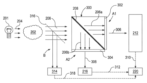
deviations,
as generally described above.
In other embodiments, however, the third
detector 314 may be arranged so as to receive electromagnetic radiation 204
directly from the electromagnetic source 201 or electromagnetic radiation
reflected off of either of the ICE 302, 304 and likewise generate the
compensating signal 318.
[0067]
The first and second output signals 310, 312 may then be
received by and computationally combined in the signal processor 220 to
determine the characteristic of interest in the sample 202. In one or more
embodiments, computationally combining the first and second output signals
310, 312 is desired. This computation may involve a variety of mathematical
relationships, including, for example, a linear relationship, a polynomial
function,
an exponential function, and or a logarithmic function, or a combination
thereof.
In these cases, a variety of normalization mathematics between the output
signals 310, 312 and the compensating signal 318 may be applied in order to
take into account any radiating deviations detected by the third detector 314.
For example, the output signals 310, 312 may each be normalized by dividing
each by the compensating signal 318 to achieve, for example, Al/B and A2/B,
before the mathematical relationship between Al/B and A2/B is applied. In
other cases, the mathematical relationship between Al and A2 may be applied,
with the resultant normalized by channel B. In even other cases, a combination
of these two normalization methods may be applied. Those skilled in the art
will
be familiar with both general methods, and can choose which method is most
applicable given the specific relationships involved. Finally, it is
understood by
those skilled in the art that fractions or multiples of the quantity B may be
employed, as well as multiplication of the quantity (1/B).
21
CA 02865641 2014-08-26
WO 2013/162744
PCT/US2013/031467
[0068]
Referring now to FIG. 3b, illustrated is another exemplary
optical computing device 320, according to one or more embodiments. The
device 320 may be substantially similar to the device 300 described above with
reference to FIG. 3a and therefore may be best understood with reference
thereto, where like numerals represent like elements not described again in
detail. In FIG. 3b, the optically interacted radiation 206 is again directed
into
the first or primary channel Al and conveyed to the first ICE 302 which
generates a first modified electromagnetic radiation 306 corresponding to the
characteristic or analyte of interest of the sample 202. The first detector
212
receives the first modified electromagnetic radiation 306 from the first ICE
302
and provides the first output signal 310.
[0069]
The second ICE 304 may again be arranged within what
could normally be used as a reference channel for the device 320 and otherwise
used to normalize the first output signal 310 derived from the primary channel
Al in view of radiating deviations of the electromagnetic radiation source
201.
Specifically, the second ICE 304 is arranged in new reference channel A2 and,
similar to the primary channel Al, may be configured to provide an output
corresponding to the characteristic or analyte of interest of the sample 202.
As
depicted, the second ICE 304 may be configured to optically interact with a
portion of the electromagnetic radiation 204 directly radiated by the
electromagnetic radiation source 201. In one or more embodiments, a beam
splitter 322 may be configured to split the electromagnetic radiation 204 and
direct a portion thereof toward the second ICE 304. In other embodiments,
however, the second ICE 304 may be arranged so as to receive the
electromagnetic radiation 204 directly from the electromagnetic radiation
source
201, instead of receiving a reflected portion thereof. Those skilled in the
art will
readily recognize that the reference channel A2 may be defined in a variety of
locations within the optical computing device 320, or any of those described
herein, without departing from the scope of the disclosure.
[0070] The
second ICE 304 generates the second modified
electromagnetic radiation 308 and conveys the same to the second detector 216.
The second detector 216 may be configured to receive and quantify the second
electromagnetic radiation 308 and provide the second output signal 312 which
may be directed toward the signal processor 220.
22
CA 02865641 2014-08-26
WO 2013/162744
PCT/US2013/031467
[0071]
As illustrated, the optical computing device 320 may further
include the third detector 314 used to detect radiating deviations stemming
from
the electromagnetic radiation source 201.
In one embodiment, the third
detector 314 may be arranged to receive a portion of the optically interacted
light 206 as reflected from the beam splitter 316. In other embodiments,
however, the third detector 314 may be arranged to receive a portion of the
electromagnetic radiation 204 as reflected from another beam splitter 324
arranged within the reflected portion of the electromagnetic radiation 204 as
derived from the first beam splitter 322. Accordingly, a true reference
channel B
may also be included in the device 300 and may serve the same purpose as the
reference channel B described above with reference to FIGS. 2a and 2b. As
illustrated, a beam splitter 316 may be arranged to reflect a portion of the
optically interacted light 206 toward the third detector 314 in order to
generate
a compensating signal 318 generally indicative of radiating deviations, as
generally described above.
[0072]
The compensating signal 318 in the second reference channel
B may be directed to the signal processor 220 and computationally combined
with the first and second output signals 310, 312 derived from the primary and
first reference channels Al, A2, respectively, in order to compensate for any
electromagnetic radiating deviations stemming from the electromagnetic
radiation source 201. As discussed above, the ratio of the light intensity
derived
from the primary and first reference channels Al, A2 is divided by the light
intensity derived from the second reference channel B, and the resulting
output
is related to the analyte concentration or characteristic of interest. In one
embodiment, for example, the compensating signal 318 and the first and second
output signals 310, 312 are combined using principal component analysis
techniques such as, but not limited to, standard partial least squares which
are
available in most statistical analysis software packages (e.g., XL Stat for
MICROSOFT EXCEL ; the UNSCRAMBLERC) from CAMO Software and
MATLABC) from MATHWORKSC)). In other embodiments, the compensating
signal 318 is used simply to inform the user of the condition of the
electromagnetic radiation source 201, e.g., whether the source 201 is
functioning properly.
[0073]
As will be appreciated by those skilled in the art, more than
two ICE 302, 304 may be used in alternative configurations or embodiments,
23
CA 02865641 2016-05-11
without departing from the scope of the disclosure. Moreover, it should be
noted that while
FIGS. 3a and 3b show electromagnetic radiation as being transmitted through
the first and
second ICE 302, 304 in order to generate the first and second modified
electromagnetic
radiations 306, 308, respectively, it is also contemplated herein to reflect
the electromagnetic
radiation off of the first and second ICE 302, 304 and equally generate the
corresponding first
and second modified electromagnetic radiations 306, 308, without departing
from the scope
of the disclosure.
[0074] It has been discovered that usage of one or more ICE in both the
primary
and reference channels Al, A2 may enhance the sensitivity and detection limits
of the optical
computing device 300 beyond what would otherwise be attainable with a single
ICE design
that utilizes a dedicated reference channel B for normalizing electromagnetic
radiation
fluctuations, such as is described above with reference to FIGS. 2a and 2b.
This was entirely
unexpected and would be considered wholly unobvious to those skilled in the
art. For
instance, the typical reference channel B in optical computing devices is a
spectrally neutral
channel and therefore dedicated solely to providing a ratio denominator useful
in normalizing
the output signal derived from the primary channel A against radiating
deviations. Placing an
ICE in the reference channel B would be wholly unobvious since the ICE is
designed to be
spectrally active and therefore has a spectrum associated with it which
optically interacts with
the second light beam 206b and changes its spectral characteristics.
Accordingly, with the
second ICE 304 arranged in the reference channel A2, as depicted in FIG. 3a,
the reference
channel is no longer used for its intended purpose but nonetheless has been
found to
dramatically increase the sensitivities and detection limits of the device
300. These
unexpected results are especially possible even in the presence of various
interferents.
100751 As further explanation, methods of how to design and build single
ICE
elements with optimal performance characteristics are disclosed in U.S. Pat.
No. 7,711,605
and U.S. Pat. Pub. No. 2010/0153048. Using the methods described therein,
literally
thousands and hundreds of thousands of individual unique designs are created
and optimized
for performance, thereby exhausting the optimal solution space available and
yielding the
best solutions possible. Those skilled in the art will readily recognize
24
CA 02865641 2014-08-26
WO 2013/162744
PCT/US2013/031467
that ICE designs can be particularly sensitive to small changes in their
optical
characteristics.
Thus, any modification of the optical characteristic (e.g.,
changes made to the particular transmission function) with, for example,
additional ICE components, would be considered as degrading the performance
of the optical computing device, and in most cases, quite rapidly with only
small
changes. And indeed, it has been discovered that spectral components (i.e.,
ICE
components or designs) arranged in the reference channel B do degrade the
overall performance in some instances.
[0076] However, it was
unexpectedly discovered that, in at least
some case, some spectral components, including some preferred ICE designs,
may enhance overall device performance when arranged in the reference
channel B. It was further discovered, that these enhancements are not minor
adjustments or improvements, but may enhance performance involving factors
and/or orders of magnitude of improvement. It was yet further discovered that
performance enhancements can be obtained without substantial compromise or
trade-off of other important characteristics. It was also discovered that the
ICE
arranged in the reference channel B may or may not be configured to be
associated with the characteristic of the sample.
[0077] Referring to FIG.
4, illustrated is a graph 400 indicating the
detection of a particular characteristic of a sample using one ICE arranged in
the
primary channel A, and another ICE in the reference channel B. It will be
appreciated that the graph 400 and the data presented therein are merely used
to facilitate a better understanding of the present disclosure, and in no way
should the they be read to limit or define the scope of the invention. The
graph
400 indicates the detection of the methane gas to oil ratio (GOR) in two
radically
different oils from concentrations from 0 to 1000 scuft/bbl (standard cubic
feet
per standard barrel) under various pressures and temperatures associated with
downhole oil field conditions. The two oils are a black, high asphaltene
content
optically opaque oil sample obtained from the Gulf of Mexico, and a light, low
asphaltene, relatively transparent, high sulfur content oil sample obtained
from
Saudi Arabia. The graph 400 depicts the accuracy (standard deviation) of
measuring the GOR for both oils across the entire 0 to 1000 scuft/bbl
concentration range of interest for an optical computing device (e.g., the
optical
device 300, or any of the exemplary optical computing devices disclosed
herein)
on the X-axis.
CA 02865641 2014-08-26
WO 2013/162744 PCT/US2013/031467
[0078]
Results are shown for five different individual ICE designs
and with the various unique combinations of the five with one of the ICE
designs
in the reference channel B. As shown, a single ICE design without an ICE in
the
reference channel B (i.e., shown as triangles) may yield an accuracy ranging
between a predictive 19.2% of full scale (190 scuft/bbl) and a non-predictive
34.9% of full scale (349 scuft/bbl).
[0079]
The sensitivity of the device (e.g., the optical device 300, or
any of the exemplary optical computing devices disclosed herein), another key
performance attribute important to the detection limits, is also shown in the
graph on the Y axis. The units of sensitivity are the absolute magnitude of
the
% change in detector signal output observed over the entire GOR concentration
range (0 to 1000 scuft/bbl) of interest. Regarding sensitivity, the larger the
magnitude of the % change, the more sensitive and desirable is the system as
greater sensitivity can enable better detectability and performance limits,
lower
costs, and other important benefits. As shown, sensitivities for the standard
configuration involving a neutral reference channel B, but without an ICE
arranged in the reference channel B (i.e., shown as triangles), range from
3.3%
to 4.9%.
[0080]
When an ICE design is arranged in the reference channel B,
however, the performance may be enhanced (i.e., shown as squares). For
example, by placing an ICE in the reference channel B, accuracies may be
improved from a non-predictive 34.9% (349scuft/bbl) to a highly predictive
1.1% (11 scuft/bbl), or about a factor of 17X improvement over the best single
ICE with neutral reference case, and about a factor of 31X over the non-
predictive case. Sensitivities
were also improved for many combinations,
obtaining a factor of between 1.5 to almost 3X of that of a single ICE design
without a spectral element (i.e., additional ICE) in the reference channel.
[0081]
Those skilled in the art will readily recognize that increases in
sensitivity are often accompanied by corresponding decreases in accuracy for
single ICE solutions. Thus, one single ICE design may have superior
sensitivity
over another, but will generally be found to be less accurate. Accuracy and
sensitivity, two of the most important performance parameters for optical
computing devices, are therefore generally trade-offs. The improvement in
accuracy discovered by using an ICE in the reference channel B, as shown in
FIG. 4, was totally unexpected. Even more unexpected was that both the
26
CA 02865641 2014-08-26
WO 2013/162744
PCT/US2013/031467
accuracy and sensitivity could be simultaneously increased or at least
maintained. For example, three of the unique combinations with an ICE in the
reference channel B show both a dramatic enhancement in accuracy and an
improvement of approximately 1.5 to 3X in sensitivity.
Three showed a
substantial improvement in sensitivity (and therefore lower detection limits)
while maintaining about the same accuracy.
[0082]
It should be noted that these unexpected results were not
achieved for all combinations of ICE designs in the reference channel B.
Instead, there were three combinations, in particular, where the accuracy
improved but the sensitivity decreased. Moreover, one combination was tested
where the accuracy was not improved, but the sensitivity decreased. However,
the graph 400 clearly shows that optical computing device performance can
increase by placing a spectral component (e.g., an ICE design) in the
reference
channel B as opposed to using the traditional non-spectral component.
Moreover, the ICE arranged in the reference channel B could either be
associated (predictive) or substantially disassociated (non-predictive) with
the
characteristic of interest (GOR in this case).
[0083]
Referring now to FIG. 5, illustrated is another exemplary
optical computing device 500, according to one or more embodiments. The
device 500 may be somewhat similar to the optical computing device 300
described above with reference to FIG. 3a, and therefore may be best
understood with reference to FIG. 3a where like numerals indicate like
elements
that will not be described again in detail. As illustrated, the device 500 may
include a first ICE 502 and a second ICE 504. The first and second ICE 502,
504
may be similar in construction to the ICE 100 described above with reference
to
FIG. 1, and configured to be either associated or disassociated with a
particular
characteristic of the sample. Embodiments are contemplated herein that include
one or more beam splitters, mirrors, and the like in order to allow the
electromagnetic radiation 204 to optically interact with both the sample 202
and
first and second ICE 502, 504, without departing from the scope of the
disclosure. Indeed, one or more beam splitters, mirrors, and the like may be
used in conjunction with any of the exemplary embodiments disclosed herein,
without departing from the scope of the disclosure.
[0084]
As illustrated, the first and second ICE 502, 504 may be
coupled together to form a monolithic structure, but in other embodiments may
27
CA 02865641 2014-08-26
WO 2013/162744
PCT/US2013/031467
be separated or otherwise arranged in series without departing from the scope
of the disclosure. Moreover, the first and second ICE 502, 504 may be arranged
to receive the optically interacted light 206, as depicted, but may equally be
arranged antecedent to the sample 202 and therefore directly receive the
electromagnetic radiation 204. In one embodiment, the first ICE 502 may be
smaller than the second ICE 504 or otherwise arranged such that a portion of
the optically interacted light 206 passes through only the second ICE 504 and
generates the first modified electromagnetic radiation 306. Another portion of
the optically interacted light 206 may pass through a combination of both the
first and second ICE 502, 504 and thereby generate the second modified
electromagnetic radiation 308. As a result, the device 500 may provide a first
or
primary channel Al that incorporates the optically interacted light 206
passing
through the second ICE 504 and thereafter generating the first modified
electromagnetic radiation 306, and a second or reference channel A2 that
incorporates the optically interacted light 206 passing through both the first
and
second ICE 502, 504 and thereafter generating the second modified
electromagnetic radiation 308.
[0085]
The first and second modified electromagnetic radiations 306,
308 may be directed to a detector 506, which may be a split or differential
detector, having a first detector portion 506a and a second detector portion
506b. In other embodiments, however, the detector 506 may be a detector
array, as known in the art, without departing from the scope of the
disclosure.
In operation, the first detector portion 506a forms part of the primary
channel
Al and may be configured to receive the first modified electromagnetic
radiation
306 and generate a first output signal 508a. Furthermore, the second detector
portion 506b forms part of the reference channel A2 and may be configured to
receive the second modified electromagnetic radiation 308 and generate a
second output signal 508b. In some embodiments, the detector 506 may be
configured to computationally combine the first and second signals 508a,b in
order to determine the characteristic of the sample, for example when using a
differential detector or quad-detector. In other embodiments, the first and
second signals 508a,b may be transmitted to or otherwise received by the
signal
processor 220 communicably coupled to the detector 506 and configured to
computationally combine the first and second output signals 508a,b in order to
determine the characteristic of the sample 202. Again, computationally
28
CA 02865641 2014-08-26
WO 2013/162744
PCT/US2013/031467
combining the first and second signals 508a,b may entail determining the ratio
of the two signals, such that a ratio of the primary channel Al against the
reference channel A2 is obtained. In some embodiments, the signal processor
220 may be a computer including a non-transitory machine-readable medium,
as generally described above.
[0086]
In at least one embodiment, the device 500 may further
include a second detector 510 that may function similarly to the third
detector
314 described above with reference to FIG. 3a, and thereby further provide a
second or true reference channel B. In operation, the detector 510 may be
arranged to receive and detect optically interacted light 512 in order to
generate
the compensating signal 318 generally indicative of radiating deviations of
the
electromagnetic radiation source 201. The compensating signal 318 may be
directed to the signal processor 220 and computationally combined with the
first
and second output signals 310, 312 in order to compensate for any
electromagnetic radiating deviations stemming from the electromagnetic
radiation source 201.
[0087]
It should be noted that even though the electromagnetic
radiation 204 is shown in FIG. 5 as optically interacting with the sample 202
before reaching the first and second ICE 502, 504, the first and second ICE
502,
504 nonetheless are considered to have optically interacted with the
electromagnetic radiation 204, albeit subsequent to the sample 202. In other
embodiments, the electromagnetic radiation 204 may optically interact with the
first and second ICE 502, 504 before reaching the sample 202, and the sample
202 nonetheless is considered to have optically interacted with the
electromagnetic radiation 204, albeit subsequent to the first and second ICE
502, 504. Furthermore, embodiments are contemplated herein where the first
ICE 502 is arranged on one side of the sample 202, and the second ICE 504 is
arranged on the opposite side of the sample 202.
As a result, the
electromagnetic radiation 204 may optically interact with the first ICE 502
prior
to optically interacting with the sample 202, and subsequently optically
interacting with the second ICE 504. It will be appreciated that any and all
of
the embodiments disclosed herein may include any of the exemplary variations
discussed herein, such as arranging the sample 202 before or after the first
and
second ICE 502, 504, or arranging the ICE 502, 504 in linear or non-linear
configurations.
29
CA 02865641 2014-08-26
WO 2013/162744
PCT/US2013/031467
[0088] Referring now to
FIG. 6, with continued reference to FIG. 5,
illustrated is another optical computing device 600, according to one or more
embodiments. The device 600
may be somewhat similar to the optical
computing device 500 described with reference to FIG. 5, therefore the device
600 may be best understood with reference thereto, where like numerals
indicate like elements. The device 600 may include a first ICE 602 and a
second
ICE 604 similar in construction to the ICE 100 described above with reference
to
FIG. 1, and configured to be either associated or disassociated with a
particular
characteristic of the sample 202, such as is described above with reference to
the first and second ICE 302, 304 of FIG. 3a.
[0089] As illustrated,
the first and second ICE 602, 604 may be
arranged generally parallel relative to one another and configured to receive
the
optically interacted light 206. As with prior embodiments, however, the first
and
second ICE 602, 604 may equally be arranged antecedent to the sample 202,
without departing from the scope of the disclosure. In operation, the first
ICE
602 may receive a portion of the optically interacted light 206 and thereby
generate the first modified electromagnetic radiation 306. The second ICE 604
may be configured to receive another portion of the optically interacted light
206
and thereby generate the second modified electromagnetic radiation 308. As a
result, the device 600 may provide a first or primary channel Al that
incorporates the optically interacted light 206 passing through the first ICE
602
and thereafter generating the first modified electromagnetic radiation 306,
and a
second or reference channel A2 that incorporates the optically interacted
light
206 passing through the second ICE 604 and thereafter generating the second
modified electromagnetic radiation 308.
[0090] The first and
second modified electromagnetic radiations 306,
308 may be directed to the detector 506 to generate the first output signal
508a
in the primary channel Al and the second output signal 508b in the reference
channel A2 as corresponding to the first and second modified electromagnetic
radiations 306, 308, respectively. Specifically, the first detector portion
506a
may be configured to receive the first modified electromagnetic radiation 306
and generate the first output signal 508a, and the second detector portion
506b
may be configured to receive the second modified electromagnetic radiation 308
and generate the second output signal 508b. In some embodiments, the
detector 506 may be configured to computationally combine the first and second
CA 02865641 2014-08-26
WO 2013/162744
PCT/US2013/031467
output signals 508a,b in order to determine the characteristic of the sample.
In
other embodiments, however, the first and second signals 508a,b may be
received by a signal processor 220 communicably coupled to the detector 506
and configured to computationally combine the first and second signals 508a,b
in
order to determine the characteristic of the sample.
[0091]
In some embodiments, the detector 506 is a single detector
but configured to time multiplex the first and second modified electromagnetic
radiations 306, 308. For example, the first ICE 602 may be configured to
direct
the first modified electromagnetic radiation 306 toward the detector 506 at a
first time Ti, and the second ICE 604 may be configured to direct the second
modified electromagnetic radiation 308 toward the detector 506 at a second
time T2, where the first and second times Ti, T2 are distinct time periods
that
do not spatially overlap. Consequently, the detector 506 receives at least two
distinct beams of modified electromagnetic radiation 306, 308 which may be
computationally combined by the detector 506 in order to provide an output in
the form of a voltage that corresponds to the characteristic of the sample.
[0092]
In one or more embodiments, in order to provide the first
and second times Ti, T2, the device 600 may include more than one
electromagnetic radiation source 201.
In other embodiments, the
electromagnetic radiation source 201 may be pulsed in order to provide the
first
and second times Ti, T2. In yet other embodiments, each ICE 602, 604 may be
mechanically positioned to interact with the electromagnetic radiation beam at
two distinct times. In yet other embodiments, the electromagnetic radiation
beam may be deflected, or diffracted to interact with the two different ICE
elements at times Ti and T2. Moreover, it will be appreciated that more than
the first and second ICE 602, 604 may be used, thereby generating additional
primary channels (e.g., A3, A4, ... An), and the detector 506 may therefore be
configured to time multiplex each additional beam of optically interacted
light to
provide the cumulative voltage corresponding to the characteristic of the
sample.
[0093] In at
least one embodiment, the device 600 may further
include the second detector 510 that may function similarly to the third
detector
314 described above with reference to FIG. 3a, and thereby further provide a
second or true reference channel B. As illustrated, a beam splitter 606 may be
arranged to reflect a portion of the optically interacted light 206 toward the
second detector 510 in order to generate a compensating signal 318 generally
31
CA 02865641 2014-08-26
WO 2013/162744
PCT/US2013/031467
indicative of radiating deviations of the electromagnetic radiation source
201. In
other embodiments, however, the second detector 510 may be arranged so as to
receive electromagnetic radiation 204 directly from the electromagnetic source
201 or electromagnetic radiation reflected off of either of the ICE 302, 304
and
likewise generate the compensating signal 318. The compensating signal 318
may be directed to the signal processor 220 and computationally combined with
the first and second output signals 310, 312 in order to compensate for any
electromagnetic radiating deviations stemming from the electromagnetic
radiation source 201. As a result, a second reference channel B may be
included
in the device 300 and employed substantially similarly to the reference
channel
B described above with reference to FIGS. 2a and 2b. In other embodiments,
the compensating signal 318 may be used to inform the user of the condition of
the electromagnetic radiation source 201, e.g., whether the source 201 is
functioning properly.
[0094]
Referring now to FIG. 7, illustrated is another optical
computing device 700, according to one or more embodiments. The device 700
may be somewhat similar to the optical computing devices 500, 600 described
with reference to FIGS. 5 and 6 and therefore the device 700 may be best
understood with reference thereto, where like numerals indicate like elements.
The device 700 may include at least two ICE, including a first ICE 702a and a
second ICE 702b, but may further include one or more additional ICE 702n.
Each ICE 702a-n may be similar in construction to the ICE 100 described above
with reference to FIG. 1, and configured to be either associated or
disassociated
with a particular characteristic of the sample 202, such as is described above
with reference to the first and second ICE 302, 304 of FIG. 3a. The device 700
may further include a plurality of detectors, such as a first detector 704a, a
second detector 704b, and one or more additional detectors 704n.
[0095]
The first, second, and additional ICE 702a-n may each be
arranged in series relative to one another and configured to optically
interact
with the electromagnetic radiation 204 either through the sample 202 or
through
varying configurations of reflection and/or transmission between adjacent ICE
702a-n. In the embodiment specifically depicted, the first ICE 702a may be
arranged in a first primary channel Al to receive the optically interacted
radiation 206 from the sample 202. As with prior embodiments, however, the
first ICE 702a may equally be arranged antecedent to the sample 202, and
32
CA 02865641 2014-08-26
WO 2013/162744
PCT/US2013/031467
therefore optically interact with the electromagnetic radiation 204. The first
ICE
702a may be configured to transmit a modified electromagnetic radiation 706a
to the first detector 704a and simultaneously convey via reflection optically
interacted light 708 toward the second ICE 702b. The second ICE 702b may be
arranged in a second primary channel A2 and configured to convey a second
optically interacted light 706b via reflection toward the second detector
704b,
and simultaneously transmit additional optically interacted light 710 toward
the
additional ICE 702n.
[0096]
The additional ICE 702n may be arranged within a reference
channel A3, which would otherwise be used to detect radiating deviations of
the
electromagnetic radiation source 201, but now is used to help determine the
characteristic of the sample 202. Accordingly, the reference channel A3 may
function substantially similarly to one of the primary channels Al, A2.
In
operation, the additional ICE 702n may be configured to convey an additional
modified electromagnetic radiation 706n via reflection toward the additional
detector 704n.
[0097]
Those skilled in the art will readily recognize numerous
alternative configurations of the first, second, and additional ICE 702a-n and
corresponding first and second primary channels Al, A2 and the reference
channel A3, without departing from the scope of the disclosure. For example,
reflection of optically interacted light from a particular ICE may be replaced
with
transmission of optically interacted light, or alternatively configurations
may
include the use of mirrors or beam splitters configured to direct the
electromagnetic radiation 204 (or optically interacted radiation 206) to each
of
the first, second, and additional ICE 702a-n.
[0098]
In at least one embodiment, the device 700 may further
include the second detector 510 that may function similarly to the third
detector
314 described above with reference to FIG. 3a, and thereby further provide a
second or true reference channel B. As illustrated, the detector 510 receives
and detects optically interacted light transmitted through the additional ICE
702n
and subsequently outputs the compensating signal 318 indicative of
electromagnetic radiating deviations. In at least one embodiment, the second
detector 510 may be communicably coupled to the signal processor 220 such
that the compensating signal 318 may be provided or otherwise conveyed
thereto.
33
CA 02865641 2014-08-26
WO 2013/162744
PCT/US2013/031467
[0099]
The first, second, and additional detectors 704a-n may be
configured to detect the first, second, and additional modified
electromagnetic
radiation 706a-n, respectively, within the corresponding first and second
primary
channels Al, A2 and the reference channel A3 and thereby generate a first
output signal 508a, a second output signal 508b, and one or more additional
output signals 508n, respectively. In some embodiments, the first, second, and
additional output signals 508a-n may be received by the signal processor 220
communicably coupled to each detector 704a-n and configured to
computationally combine the first, second, and additional signals 508a-n in
order
to determine the characteristic of the sample 202.
[00100]
This computation may involve a variety of mathematical
relationships, including, for example, a linear relationship, a polynomial
function,
an exponential function, and/or a logarithmic function, or a combination
thereof.
In these cases, a variety of normalization mathematics between the output
signals 508a, 508b...508n and the compensating signal 318 may be applied. For
example, the output signals 508a, 508b...508n may each be normalized by
dividing them each by the compensating signal 318 to achieve, for example,
Al/B, A2/B...A3/B, before the mathematical relationship between Al/B and A2/B
is applied. In other cases, the mathematical relationship between Al and A2
may be applied, with the result normalized by B. In even other cases, a
combination of these two normalization methods may be applied. Those skilled
in the art will be familiar with both general methods, and can choose which
method is most applicable given the specific relationships involved. In one
embodiment, for example, the compensating signal 318 and the output signals
508a, 508b, ...508n are combined using
principal component analysis
techniques such as, but not limited to, standard partial least squares which
are
available in most statistical analysis software packages (e.g., XL Stat for
MICROSOFT EXCEL ; the UNSCRAMBLERC) from CAMO Software and
MATLABC) from MATHWORKSC)). Finally, it is understood by those skilled in the
art that fractions or multiples of the quantity B may be employed, as well as
multiplication of the quantity (1/B).
[00101]
As will be appreciated, any number of ICE may be arranged
within any number of primary channels or otherwise used in series in order to
determine the characteristic of the sample 202. In some embodiments, each of
the first, second, and additional ICE 702a-n may be specially-designed to
detect
34
CA 02865641 2014-08-26
WO 2013/162744 PCT/US2013/031467
the particular characteristic of interest or otherwise be configured to be
associated therewith. In other embodiments, however, one or more of the first,
second, and additional ICE 702a-n may be configured to be disassociated with
the particular characteristic of interest, and/or otherwise may be associated
with
an entirely different characteristic of the sample 202.
In yet other
embodiments, each of the first, second, and additional ICE 702a-n may be
configured to be disassociated with the particular characteristic of interest,
and
otherwise may be associated with an entirely different characteristic of the
sample 202.
[00102] Referring now to FIG. 8, illustrated is an alternative
configuration of the optical computing device 700, according to one or more
embodiments. In FIG. 8, a series of beam splitters 711a, 711b, 711n may be
added to the first and second primary channels Al, A2 and the reference
channel
A3, respectively, and used to separate or otherwise redirect the optically
interacted radiation 206 As depicted, each beam splitter 711a-n may be
configured to produce and direct a respective beam 712a, 712b, 712n of
optically interacted radiation 206 toward a corresponding ICE 702a-n. Each ICE
702a-n may then be configured to transmit its respective modified
electromagnetic radiation 706a-n toward a corresponding detector 704a-n,
thereby generating the first, second, and additional output signals 508a-n,
respectively. The first, second, and additional signals 508a-n may then be
received by a signal processor 220 communicably coupled to each detector
704a-n and configured to computationally combine the first, second, and
additional signals 508a-n in order to determine the characteristic of the
sample
202.
[00103] In some
embodiments, the second detector 510 may again
be used in the second or true reference channel B to detect electromagnetic
radiating deviations exhibited by the electromagnetic radiation source 201,
and
thereby normalize the signals 508a-n produced by the detectors 704a-n. The
second detector 510 may be communicably coupled to the signal processor 220
such that the compensating signal 318 indicative of electromagnetic radiating
deviations may be provided or otherwise conveyed thereto. The signal processor
220 may then be configured to computationally combine the compensating
signal 318 with the signals 508a-n, and thereby normalize the signals 508a-n
and provide a more accurate determination of the characteristic of the sample.
CA 02865641 2014-08-26
WO 2013/162744 PCT/US2013/031467
[00104] Referring now to
FIG. 9, illustrated is yet another alternative
configuration of the optical computing device 700, according to one or more
embodiments. As illustrated in FIG. 9, the optically interacted radiation 206
may
be fed into or otherwise provided to, for example, an optical light pipe 714.
The
optical light pipe 714 may be configured to convey the optically interacted
radiation 206 individually to each of the first and second primary channels
Al,
A2 and the reference channel A3. In some embodiments, the optical light pipe
714 may be a fiber optic bundle having a plurality of corresponding conveying
bundles. In operation, a first bundle 714a may be configured to convey
optically
interacted radiation 206 to the first ICE 702a in the first primary channel Al
in
order to generate the modified electromagnetic radiation 706a; a second bundle
714b may be configured to convey optically interacted radiation 206 to the
second ICE 702b in the second primary channel A2 in order to generate the
second optically interacted light 706b; and an additional bundle 714n may be
configured to convey optically interacted radiation 206 to the additional ICE
702n in the reference channel A3 in order to generate the additional modified
electromagnetic radiation 706n. At least one additional bundle 714x may be
configured to convey optically interacted radiation 206 to the second detector
510 in the second or true reference channel B in order to generate the
compensating signal 318. Processing of the resulting modified electromagnetic
radiation 706a-n and signals 508a-n may be accomplished as generally
described above.
[00105] It should be noted
that the use of optical light pipes, such as
the optical light pipe 714 discussed above, may be employed in any of the
various embodiments and combinations discussed herein, without departing
from the scope of the disclosure. Use of a light pipe, or a variation thereof,
may
prove advantageous in that the light pipe substantially removes interferent
obstruction that may otherwise contaminate the optically interacted radiation
206 provided to the various ICEs.
[00106] Referring now to
FIG. 10, illustrated is another optical
computing device 1000, according to one or more embodiments. The device
1000 may be somewhat similar to the optical computing device 300 and 320
described with reference to FIGS. 3a and 3b and therefore the device 1000 may
be best understood with reference thereto, where like numerals indicate like
elements. The device 1000 may include a movable assembly 1002 having at
36
CA 02865641 2014-08-26
WO 2013/162744 PCT/US2013/031467
least two ICEs associated therewith and various corresponding primary channels
and at least one reference channel. As illustrated, the movable assembly 1002
may be characterized at least in one embodiment as a rotating disc 1003,
wherein the at least two ICEs are radially disposed for rotation therewith.
Alternatively, the movable assembly 1002 may be characterized as a linear
array
1005, wherein the at least two ICEs are laterally offset from each other. FIG.
10
illustrates corresponding side and frontal views of both the rotating disc
1003
and the linear array 1005, each of which is described in more detail below.
[00107] Those skilled in
the art will readily recognize, however, that
the movable assembly 1002 may be characterized as any type of movable
assembly configured to sequentially align at least one detector with optically
interacted light 206 and/or one or more ICE. For example, the movable
assembly 1002 may include such apparatus or devices as, but not limited to, an
oscillating or translating linear array of ICE, one or more scanners, one or
more
beam deflectors, combinations thereof, or the like. In other embodiments, the
movable assembly 1002 may be characterized as an assembly including a
plurality of optical light pipes (e.g., fiber optics) configured to perform
optical
beam splitting to a fixed array of ICE and/or detectors.
[00108] Varying
embodiments of the rotating disc 1003 may include
any number of ICE arranged about or near the periphery of the rotating disc
1003 and circumferentially-spaced from each other. In the illustrated
embodiment, the rotating disc 1003 includes a first ICE 1004a, a second ICE
1004b, a third ICE 1004c, and a fourth ICE 1004d, but it will be appreciated
that
the rotating disc 1003 may also include any number of additional ICE 1004n as
needed for the particular application. Each ICE 1004a-n may be similar in
construction to the ICE 100 described above with reference to FIG. 1, and
configured to be either associated or disassociated with a particular
characteristic of the sample 202, such as is described above with reference to
the first and second ICE 302, 304 of FIG. 3a. In various embodiments, the
rotating disc 1003 may be rotated at a frequency of about 0.1 RPM to about
30,000 RPM.
[00109] In operation, the
rotating disc 1003 may rotate such that
each individual ICE 1004a-n may be exposed to or otherwise optically interact
with the optically interacted radiation 206 for a distinct brief period of
time. In
at least one embodiment, however, the movable assembly 1002 may be
37
CA 02865641 2014-08-26
WO 2013/162744 PCT/US2013/031467
arranged antecedent to the sample 202 such that each ICE 1004a-n may be
exposed to or otherwise optically interact with the electromagnetic radiation
204
for a brief period of time. Upon optically interacting with the optically
interacted
radiation 206 each ICE 1004a-n may be configured to produce modified
electromagnetic radiation, for example, a first modified electromagnetic
radiation
1006a emanating from the first ICE 1004a, a second modified electromagnetic
radiation 1006b emanating from the second ICE 1004b, a third modified
electromagnetic radiation 1006c emanating from the third ICE 1004c, a fourth
modified electromagnetic radiation 1006d emanating from the fourth ICE 1004d,
and an additional modified electromagnetic radiation 1006n emanating from the
one or more additional ICE 1004n.
[00110] As each individual
ICE 1004a-n aligns with the optically
interacted light 206 to produce the modified electromagnetic radiations 1106a-
n,
respectively, corresponding first, second, third, and fourth primary channels
Al,
A2, A3, and A4 and one or more reference channels Bn are thereby generated.
Since the device 1000 is not necessarily limited to any specific number of ICE
1004a-n, a corresponding number of primary channels may also be defined by
the device 1000 (e.g., primary channel(s) An). Moreover, it will be
appreciated
that, while the rotating disc 1003 may include any number of additional ICE
1004n as needed, any number of corresponding or otherwise unrelated
reference channels B may also be included in the device 1000 (e.g., reference
channels Bl, B2...Bn), without departing from the scope of the disclosure.
Whereas at least one of the one or more reference channels B would otherwise
be configured to detect radiating deviations of the electromagnetic radiation
source 201, embodiments are contemplated herein where a spectrally active
additional ICE 1004n is arranged within said reference channel B. As a result,
the reference channel B may serve substantially the same purpose as the first,
second, third, and fourth primary channels Al, A2, A3, A4 by detecting and
determining the characteristic of the sample 202.
[001 1 1] In one or more
embodiments, however, at least one of the
one or more reference channels B (e.g., Bl, B2,...Bn) may include a neutral
spectral element (not shown) configured to simply pass the optically
interacted
radiation 206 without optical-interaction. As a result, the neutral element
may
be configured to provide a neutral signal to the detector 212 that may be
substantially similar to the compensating signal 318 as described above with
38
CA 02865641 2014-08-26
WO 2013/162744 PCT/US2013/031467
reference to FIG. 3a, and thereby generate a true reference channel B, as
generally described herein. In operation, the detector 212 may detect the
neutral signal which may be indicative of radiating deviations stemming from
the
electromagnetic radiation source 201.
[00112] Each beam of
modified electromagnetic radiation 1006a-n
may be detected by the detector 212 which may be configured to time multiplex
the modified electromagnetic radiation 1006a-n between the individually-
detected beams. For example, the first ICE 1004a may be configured to direct
the first modified electromagnetic radiation 1006a toward the detector 212 at
a
first time Ti, the second ICE 1004b may be configured to direct the second
modified electromagnetic radiation 1006b toward the detector 212 at a second
time T2, and so on until the one or more additional ICE 1004n may be
configured to direct the additional modified electromagnetic radiation 1006
toward the detector 212 at an additional time Tn. Consequently, the detector
212 receives a plurality of distinct beams of modified electromagnetic
radiation
1006a-n which may be computationally combined by the detector 212 in order
to provide an output in the form of a voltage that corresponds to the
characteristic of the sample. In some embodiments, these beams of modified
electromagnetic radiation 1006a-n may be averaged over an appropriate time
domain (e.g., about 1 millisecond to about 1 hour) to more accurately
determine
the characteristic of the sample 202.
[00113] The time
multiplexed computation from the various primary
channels Al, A2,...An and reference channel(s) B (e.g., Bl, B2,...Bn) may
involve
a variety of mathematical relationships, including, for example, a linear
relationship, a polynomial function, an exponential function, and or a
logarithmic
function, or a combination thereof. In these cases, a variety of normalization
mathematics between the primary channels Al, A2,...An and reference
channel(s) B may be applied. For example, the signals Al, A2,...An may each be
normalized by dividing them each by Bl, B2,...Bn (or a mathematical
combination of Bl, B2,...Bn) to achieve, for example, Al/B, A2/B...An/B,
before
the mathematical relationship between Al/B and A2/B is applied. In other
cases, the mathematical relationship between Al, A2,...An may be applied, with
the resultant normalized by Bl, B2...Bn (or a mathematical combination of Bl,
B2...Bn).
In even other cases, a combination of these two normalization
methods may be applied. Those skilled in the art will be familiar with both
39
CA 02865641 2014-08-26
WO 2013/162744 PCT/US2013/031467
general methods, and can choose which method is most applicable given the
specific relationships involved.
In one embodiment, for example, the
compensating signal Bl, B2...Bn
and the output signals Al, A2...An are
combined using principal component analysis techniques such as, but not
limited to, standard partial least squares which are available in most
statistical
analysis software packages (e.g., XL Stat for MICROSOFT EXCEL ; the
UNSCRAMBLERC) from CAMO Software and MATLABC) from MATHWORKSC)).
Finally, it is understood by those skilled in the art that fractions or
multiples of
the quantity B may be employed, as well as multiplication of the quantity
(1/B).
[00114] As will be
appreciated, each of the ICE 1004a-n may be
specially-designed to detect or otherwise configured to be associated with the
particular characteristic of interest. In other embodiments, however, one or
more of the ICE 1004a-n may be configured to be disassociated with the
particular characteristic of interest, and otherwise may be associated with an
entirely different characteristic of the sample 202. In yet other embodiments,
each of the one or more ICE 1004a-n may be configured to be disassociated with
the particular characteristic of interest, and otherwise may be associated
with an
entirely different characteristic of the sample 202. Advantages of this
approach
can include the ability to analyze multiple analytes in multiple respective
channels using a single optical computing device and the opportunity to assay
additional analytes simply by adding additional ICEs to the rotating disc
1003.
[00115] The linear array
1005 may also include the first, second,
third, and fourth ICE 1004a-d and the one or more additional ICE 1004n,
although aligned linearly as opposed to radially positioned. The linear array
1005 may be configured to oscillate or otherwise translate laterally or
vertically
such that each ICE 1004a-n is exposed to or otherwise able to optically
interact
with the optically interacted radiation 206 for a distinct brief period of
time.
Similar to the rotating disc 1003, the linear array 1005 may be configured to
produce modified electromagnetic radiation 1006a-n. Again, as each individual
ICE 1004a-n aligns with the optically interacted light 206 to produce the
modified electromagnetic radiations 1106a-n, respectively, corresponding
first,
second, third, and fourth primary channels Al, A2, A3, and A4 and one or more
reference channels B (e.g., Bl, B2,...Bn) are thereby generated. As will be
appreciated, any number of ICE 1004a-n may be arranged on the linear array
1005 in order to determine the characteristic of the sample 202, and therefore
CA 02865641 2014-08-26
WO 2013/162744 PCT/US2013/031467
any number of corresponding primary channels A1-A4 and additional reference
channels B may also be generated.
[00116] Moreover, as with
the rotating disc 1003 embodiment, the
detector 212 may be configured to time multiplex the modified electromagnetic
radiation 1006a-n between the individually-detected beams and subsequently
provide an output in the form of a voltage that corresponds to the
characteristic
of the sample 202. Even further, at least one of the ICE 1004a-n may be a
neutral element configured to provide a neutral signal to the detector 212 in
a
true reference channel B that may be computationally combined with the
remaining beams of modified electromagnetic radiation 1006a-n to compensate
for electromagnetic radiating deviations stemming from the electromagnetic
radiation source 201.
[00117] Referring now to
FIG. 11, with continued reference to FIG.
10, illustrated is another exemplary optical computing device 1100, according
to
one or more embodiments. The device 1100 may be somewhat similar to the
device 1000 of FIG. 10, and therefore may be best understood with reference
thereto where like numerals indicate like elements. The device 1100 may
include a movable assembly 1102 similar in some respects to the movable
assembly 1002 of FIG. 10. For example, FIG. 11 illustrates an alternative
embodiment of a rotating disc 1103. The rotating disc 1103 in FIG. 11,
however, may include multiple radially-offset rows or arrays of ICE, such as a
first radial array 1104a, a second radial array 1104b, and one or more
additional
radial arrays 1104n. Accordingly, while three radial arrays 1104a, 1104b, and
1104n are shown in FIG. 11, it will be appreciated that the rotating disc 1103
may include more or less than three arrays 1104a-n, without departing from the
scope of the disclosure.
[00118] Each radially-
offset radial array 1104a-n may include a
plurality of ICE 1106 circumferentially-spaced from each other. Again, while a
particular number of ICE 1106 are specifically depicted in FIG. 11, it should
be
appreciated that any number of ICE 1106 may be used in the rotating disc 1103,
without departing from the scope of the disclosure. Each ICE 1106 may be
similar in construction to the ICE 100 described above with reference to FIG.
1,
and configured to be either associated or disassociated with a particular
characteristic of the sample 202, such as is described above with reference to
the first and second ICE 302, 304 of FIG. 3a. In operation, the rotating disc
41
CA 02865641 2014-08-26
WO 2013/162744 PCT/US2013/031467
1103 rotates such that the one or more ICE 1106 may each be exposed to or
otherwise optically interact with the optically interacted radiation 206 for a
distinct brief period of time. In at least one embodiment, however, the
rotating
disc 1103 may be arranged antecedent to the sample 202, and therefore the one
or more ICE 1106 may be exposed to or otherwise optically interact with the
electromagnetic radiation 204 for a brief period of time.
Upon optically
interacting with the optically interacted radiation 206, each ICE 1106 may be
configured to produce an individual or combined beam of modified
electromagnetic radiation 1008 directed toward the detector 212. Moreover, as
each individual ICE 1106 aligns with the optically interacted light 206 to
produce
corresponding modified electromagnetic radiations 1008, several distinct
primary
channels for conveying and detecting light are generated, and at least one
reference channel is generated that may operate substantially similarly to a
primary channel since an ICE 1106 is arranged therein as opposed to a
traditional neutral element.
[00119] Each individual or combined beam of modified
electromagnetic radiation 1008 may be detected by the detector 212 which may
be configured to time multiplex the modified electromagnetic radiation 1008
between the combined or individually-detected beams in each primary and
reference channel. Consequently, the detector 212 receives a plurality of
beams
of modified electromagnetic radiation 1008 which may be computationally
combined by the detector 212 in order to provide an output in the form of a
voltage that corresponds to the characteristic of the sample. Moreover, one or
more of the ICE 1106 may be a neutral element or otherwise an aperture may
be defined in the rotating disc 1103 and configured to provide a neutral
signal to
the detector 212, and thereby provide a true reference channel, as generally
described above with reference to FIG. 10. The neutral signal may be
indicative
of radiating deviations stemming from the electromagnetic radiation source
201,
and the detector 212 may be configured to computationally combine the neutral
signal with the remaining beams of modified electromagnetic radiation 1008 to
compensate for electromagnetic radiating deviations stemming from the
electromagnetic radiation source 201, and thereby provide a more accurate
determination of the characteristic of the sample.
[00120] While the various
embodiments disclosed herein provide that
the electromagnetic radiation source 201 is used to provide electromagnetic
42
CA 02865641 2016-05-11
radiation that optically interacts with the at least two ICEs, those skilled
in the art will readily
recognize that electromagnetic radiation may be derived from the sample 202
itself, and
otherwise derived independent of the electromagnetic radiation source 201. For
example,
various substances naturally radiate electromagnetic radiation that is able to
optically interact
with the at least two ICEs. In some embodiments, the sample 202 may be a
blackbody
radiating substance configured to radiate heat that may optically interact
with the at least two
ICEs. In other embodiments, the sample 202 may be radioactive or chemo-
luminescent and
therefore radiate electromagnetic radiation that is able to optically interact
with the at least
two ICEs. In yet other embodiments, the electromagnetic radiation may be
induced from the
sample 202 by being acted upon mechanically, magnetically, electrically,
combinations
thereof, or the like. For instance, in at least one embodiment a voltage may
be placed across
the sample 202 in order to induce the electromagnetic radiation. As a result,
embodiments are
contemplated herein where the electromagnetic radiation source 201 is entirely
omitted from
the particular optical computing device.
[00121]
Therefore, the present invention is well adapted to attain the ends and
advantages mentioned as well as those that are inherent therein. The
particular embodiments
disclosed above are illustrative only, as the present invention may be
modified and practiced
in different but equivalent manners apparent to those skilled in the art
having the benefit of
the teachings herein. Furthermore, no limitations are intended to the details
of construction or
design herein shown, other than as described in the claims below. It is
therefore evident that
the particular illustrative embodiments disclosed above may be altered,
combined, or
modified and all such variations are considered within the scope of the
appended claims.
While compositions and methods are described in terms of "comprising,"
"containing," or
"including" various components or steps, the compositions and methods can also
"consist
essentially of' or "consist of' the various components and steps. All numbers
and ranges
disclosed above may vary by some amount. Whenever a numerical range with a
lower limit
and an upper limit is disclosed, any number and any included range falling
within the range is
specifically disclosed. In particular, every range of values (of the form,
"from about a to
about b," or, equivalently, "from approximately a to b," or, equivalently,
"from approximately
a-b") disclosed herein is to be understood to set forth every number and range
encompassed
43
CA 02865641 2016-05-11
within the broader range of values. Also, the terms in the claims have their
plain, ordinary
meaning unless otherwise explicitly and clearly defined by the patentee.
Moreover, the
indefinite articles "a" or "an," as used in the claims, are defined herein to
mean one or more
than one of the element that it introduces. If there is any conflict in the
usages of a word or
term in this specification and one or more patent or other documents that may
be herein
referred to the definitions that are consistent with this specification should
be adopted.
44