Note: Descriptions are shown in the official language in which they were submitted.
CA 02865811 2014-08-27
WO 2013/138132
PCT/US2013/029305
METAL OXIDE CHARGE TRANSPORT MATERIAL
DOPED WITH ORGANIC MOLECULES
TECHNICAL FIELD
[0001] The present disclosure relates to the field of organic
semiconductors and more
particularly to organic films for use in organic electronic devices.
BACKGROUND
[0002] Optoelectronic devices rely on the optical and electronic properties
of materials to
either produce or detect electromagnetic radiation electronically or to
generate electricity
from ambient electromagnetic radiation. Optoelectronic devices that make use
of organic
semiconductor materials are becoming more desirable because of their potential
for cost
advantage over inorganic semiconductor materials and certain beneficial
inherent properties
organic materials, such as their flexibility.
[0003] Photosensitive optoelectronic devices convert electromagnetic
radiation into an
electrical signal or electricity. Solar cells, also called photovoltaic ("PV")
devices, are a type
of photosensitive optoelectronic devices that are specifically used to
generate electrical
power. An organic photosensitive device comprises at least one photoactive
region in which
light is absorbed to form an exciton, which may subsequently dissociate into
an electron and
a hole. The photoactive region will typically comprise a donor-acceptor
heterojunction, and
is a portion of a photosensitive device that absorbs electromagnetic radiation
to generate
excitons that may dissociate in order to generate an electrical current. The
donor-acceptor
heterojunction can be a planar heterojunction, bulk heterojunction, or
hybridized mixed-
planar heterojunction. A hybridized mixed-planar heterojunction comprises a
first organic
layer comprising a mixture of an organic acceptor material and an organic
donor material;
and a second organic layer comprising an unmixed layer of the organic acceptor
material or
the organic donor material of the first organic layer. Such hybridized mixed-
planar
heterojunction is described in United States patent application Publication
No. 2005/0224113
of Xue, et al., published on October 13, 2005, the contents of which are
incorporated herein
by reference in its entirety.
[0004] An organic photosensitive optoelectronic device may also comprise
transparent
charge transfer layers, electrodes, or charge recombination zones. A charge
transfer layer
may be organic or inorganic, and may or may not be photoconductively active. A
charge
transfer layer is similar to an electrode, but does not have an electrical
connection external to
CA 02865811 2014-08-27
WO 2013/138132
PCT/US2013/029305
the device and only delivers charge carriers from one subsection of an
optoelectronic device
to the adjacent subsection. A charge recombination zone is similar to a charge
transfer layer,
but allows for the recombination of electrons and holes between adjacent
subsections of an
optoelectronic device. Charge recombination zones are described, for example,
in U.S.
Patent No. 6,657,378 to Forrest et al.; Published U.S. Patent Application 2006-
0032529 Al,
entitled "Organic Photosensitive Devices" by Rand et al., published February
16, 2006; and
Published U.S. Patent Application 2006-0027802 Al, entitled "Stacked Organic
Photosensitive Devices" by Forrest et al., published February 9, 2006; each
incorporated
herein by reference for its disclosure of recombination zone materials and
structures. A
charge recombination zone may or may not include a transparent matrix layer in
which the
recombination centers are embedded. A charge transfer layer, electrode, or
charge
recombination zone may serve as a cathode and/or an anode of subsections of
the
optoelectronic device. An electrode or charge transfer layer may serve as a
Schottky contact.
[0005] For additional background explanation and description of the state
of the art for
organic photosensitive devices, including their general construction,
characteristics,
materials, and features, U.S. Patent Nos. 6,972,431, 6,657,378 and 6,580,027
to Forrest et al.,
and U.S. Patent No. 6,352,777 to Bulovic et al., are incorporated herein by
reference in their
entireties.
[0006] In the context of organic materials, the terms "donor" and
"acceptor" refer to the
relative positions of the Highest Occupied Molecular Orbital ("HOMO") and
Lowest
Unoccupied Molecular Orbital ("LUMO") energy levels of two contacting but
different
organic materials. If the HOMO and LUMO energy levels of one material in
contact with
another are lower, then that material is an acceptor. If the HOMO and LUMO
energy levels
of one material in contact with another are higher, then that material is a
donor. It is
energetically favorable, in the absence of an external bias, for electrons at
a donor-acceptor
junction to move into the acceptor material.
[0007] As used herein, a first HOMO or LUMO energy level is "higher than" a
second
HOMO or LUMO energy level if the first energy level is closer to the vacuum
energy level
and the first HOMO or LUMO energy level is "lower than" a second HOMO or LUMO
energy level if the first energy level is further away from the vacuum energy
level. A higher
HOMO energy level corresponds to an ionization potential having a smaller
absolute energy
relative to a vacuum level. Similarly, a higher LUMO energy level corresponds
to an
electron affinity having a smaller absolute energy relative to vacuum level.
On a
2
CA 02865811 2014-08-27
WO 2013/138132
PCT/US2013/029305
conventional energy level diagram, with the vacuum level at the top, the LUMO
energy level
of a material is higher than the HOMO energy level of the same material.
[0008] A significant property in organic semiconductors is carrier
mobility. Mobility
measures the ease with which a charge carrier can move through a conducting
material in
response to an electric field. In the context of organic photosensitive
devices, a material that
conducts preferentially by electrons due to high electron mobility may be
referred to as an
electron transport material. A material that conducts preferentially by holes
due to a high
hole mobility may be referred to as a hole transport material. A layer that
conducts
preferentially by electrons, due to mobility and/or position in the device,
may be referred to
as an electron transport layer. A layer that conducts preferentially by holes,
due to mobility
and/or position in the device, may be referred to as a hole transport layer.
Preferably, but not
necessarily, an acceptor material is an electron transport material and a
donor material is a
hole transport material.
[0009] As used herein, the term "organic" includes polymeric materials as
well as small
molecule organic materials that may be used to fabricate organic opto-
electronic devices.
"Small molecule" refers to any organic material that is not a polymer, and
"small molecules"
may actually be quite large. Small molecules may include repeat units in some
circumstances. For example, using a long chain alkyl group as a substitute
does not remove a
molecule from the "small molecule" class. Small molecules may also be
incorporated into
polymers, for example as a pendent group on a polymer backbone or as a part of
the
backbone. Small molecules may also serve as the core moiety of a dendrimer,
which consists
of a series of chemical shells built on the core moiety. The core moiety of a
dendrimer may
be a fluorescent or phosphorescent small molecule emitter. A dendrimer may be
a "small
molecule." In general, a small molecule has a defined chemical formula with a
molecular
weight that is the same from molecule to molecule, whereas a polymer has a
defined
chemical formula with a molecular weight that may vary from molecule to
molecule. As
used herein, "organic" includes metal complexes of hydrocarbyl and heteroatom-
substituted
hydrocarbyl ligands.
[0010] An example of organic optoelectronic devices that produce
electromagnetic
radiation electronically include organic light emitting devices (OLEDs). OLEDs
make use of
thin organic films that emit light when voltage is applied across the device.
OLEDs are
becoming an increasingly interesting technology for use in applications such
as flat panel
displays, illumination, and backlighting. Several OLED materials and
configurations are
3
CA 02865811 2014-08-27
WO 2013/138132
PCT/US2013/029305
described in U.S. Pat. Nos. 5,844,363, 6,303,238, and 5,707,745, the
disclosures of which are
incorporated herein by reference in their entireties.
[0011] OLED devices are often configured to emit light through at least one
of the
electrodes, and one or more transparent electrodes may be useful in an organic
opto-
electronic devices. For example, a transparent electrode material, such as
indium tin oxide
(ITO), may be used as the bottom electrode. A transparent top electrode, such
as disclosed in
U.S. Pat. Nos. 5,703,436 and 5,707,745, which are incorporated herein by
reference in their
entireties, may also be used. For a device intended to emit light only through
the bottom
electrode, the top electrode does not need to be transparent, and may include
a thick and
reflective metal layer having a high electrical conductivity. Similarly, for a
device intended
to emit light only through the top electrode, the bottom electrode may be
opaque and/or
reflective. This is because, where an electrode does not need to be
transparent, using a
thicker layer may provide better conductivity, and using a reflective
electrode may increase
the amount of light emitted through the other electrode, by reflecting light
back towards the
transparent electrode. Fully transparent devices may also be fabricated, where
both
electrodes are transparent.
[0012] In many color display applications, three OLEDs, each emitting light
of one of the
three primary colors, blue, green and red, are arranged in a stack, thereby
forming a color
pixel from which any color can be emitted. Examples of such stacked OLED
("SOLED")
structures can be found described in PCT International Application WO 96/19792
and U.S.
Pat. No. 6,917,280, the disclosures of which are incorporated herein by
reference in their
entireties.
[0013] In such a stacked structure, a pair of electrode layers are
provided, one at the
bottom and another at the top of the SOLED stack. In one variation of SOLEDs,
an
intermediate electrode layer that is externally connected can be provided
between each of the
OLED units in the stack. In other variations of SOLEDs, a charge generating
layer ("CGL")
that injects charge carriers but without direct external electrical connection
is provided
between each of the OLED units in the stack.
[0014] As used herein, "top" means furthest away from the optoelectronic
device's
substrate, while "bottom" means closest to the substrate. For example, for a
device having
two electrodes, the bottom electrode is the electrode closest to the
substrate, and is generally
the first electrode fabricated. The bottom electrode has two surfaces, a
bottom surface closest
to the substrate, and a top surface further away from the substrate. Where a
first layer is
4
CA 02865811 2014-08-27
WO 2013/138132
PCT/US2013/029305
described as "disposed over" a second layer, the first layer is disposed
further away from
substrate but not necessarily in physical contact with the second layer. There
may be one or
more other layers between the first and second layers, unless it is specified
that the first layer
is "in physical contact with" the second layer. For example, a cathode may be
described as
being "disposed over" an anode, even though there are various layers in
between.
SUMMARY
[0015] The present disclosure provides a charge transport material for use
in an
optoelectronic device comprising a metal oxide doped with an organic compound.
According
to an embodiment of the present disclosure, some examples of the organic
material for
doping are 2,3,5,6-tetrafluoro-7,7,8,8-tetracyanoquinodimethane (F4TCNQ),
acridine orange
base (AOB), and chloroboron subphthalocyanine (SubPc).
[0016] According to another embodiment, an optoelectronic device
incorporating such
charge transport material is disclosed. Such device can be a photosensitive
device
comprising a first electrode, a second electrode, a photoactive region
disposed between the
first electrode and the second electrode and electrically connected to the
first and second
electrodes, and a charge transport layer disposed between the photoactive
region and at least
one of the first and second electrodes, wherein the charge transport layer
comprises a metal
oxide material that is doped with an organic dopant material.
[0017] The metal oxide material doped with organic compounds having
decreased
resistivity can be used as either a hole-transport layer ("HTL"), an electron
transport layer
("ETL"), or both, in organic photovoltaic devices ("OPV"). The metal oxide
material can
also be used as a recombination zone in tandem OPVs, or as charge transport
layers in
OLEDs or CGLs in SOLEDs.
[0018] According to an embodiment, an OLED comprises an anode, a cathode,
and at
least one emissive layer and at least one charge transport layer disposed
between the anode
and the cathode. In this embodiment, the at least one charge transport layer
comprises a
metal oxide material doped with an organic dopant material.
[0019] In another embodiment, a SOLED comprises an anode, a cathode, a
plurality of
emissive regions disposed between the anode and the cathode, and a CGL
disposed between
successive emissive regions. In this embodiment, the CGL comprises a metal
oxide material
doped with an organic dopant material.
CA 02865811 2014-08-27
WO 2013/138132
PCT/US2013/029305
[0020] The present invention also provides a method of making the disclosed
charge
transport material for use in an optoelectronic device comprising a metal
oxide and an
organic dopant material. Examples of making such doped metal oxide
compositions include
vacuum thermal evaporation, solution deposition, spin casting, spray coating,
doctor-blading,
and other solution processing techniques.
BRIEF DESCRIPTION OF THE DRAWINGS
[0021] FIG. 1 is a cross-sectional view of an organic photovoltaic device
according to an
embodiment.
[0022] FIG. 2 is a cross-sectional view of an organic photovoltaic device
according to
another embodiment.
[0023] FIG. 3 is a cross-sectional view of a two layer organic light
emitting device.
[0024] FIG. 4 is a cross-sectional view of a three layer organic light
emitting device.
[0025] FIG. 5 is a cross-sectional view of a stacked organic light emitting
device.
[0026] FIG. 6 Resistivity of Mo03 films doped with AOB, measured from
ITO/Mo03:A0B/Au sandwich-type devices.
[0027] FIGS. 7a and 7b show absorption coefficients of various doped Mo03
films
deposited on quartz.
[0028] FIGS. 8a and 8b show dark (8a) and one-sun illuminated (8b) plots of
the J-V
characteristics of OPVs incorporating Mo03 layers doped with Ag, F4TCNQ, and
AOB.
[0029] FIGS. 9a and 9b show one-sun illuminated J-V characteristics (9a)
and
performance parameters (9b) of OPV devices as a function of AOB doping
concentration.
[0030] FIGS. 10a and 10b show dark J-V characteristics (10a) and series
resistance (10b)
of OPV devices as a function of AOB doping concentration.
[0031] FIGS. lla and llb show one-sun illuminated J-V characteristics (11
a) and
performance parameters (1 lb) of OPV devices comparing different buffer
layers.
[0032] Except where noted otherwise, all drawings are schematic and are not
drawn to
scale and are not intended to necessarily convey actual dimensions.
DETAILED DESCRIPTION
[0033] New metal oxide charge transport materials doped with organic
molecules to
increase the conductivity of the metal oxide thin films is disclosed. The
resulting charge
transport material exhibit increased conductivity, optical transparency, light
absorption, and
6
CA 02865811 2014-08-27
WO 2013/138132
PCT/US2013/029305
chemical resistance suitable for optoelectronic devices. They can be used for
either a HTL,
an ETL, or both, in an OPV device or OLED devices. Other applications of the
disclosed
composition include uses as a recombination zone in tandem OPVs, or as a
charge generation
layers in SOLEDs.
[0034] As described herein, "metal oxide" may be any transition metal oxide
which have
favorable energy level alignment, electric conductivity, optical transparency,
and chemical
robustness. The metal oxides are suitable as charge transport layers in
organic and molecular
electronics. They may have abilities to provide good energy level alignment
with a wide
range of materials to improve carrier injection and extraction. Their optical
transparency may
allow their use as optical spacers. They are compatible with a wide range of
deposition
processes such as vacuum evaporation, solution deposition, spin casting, spray
coating,
doctor-blading, and other solution processing techniques. They also have
chemical resistance
allowing the subsequent solvent-based deposition of subsequent layers.
Examples of the
metal oxide material include Mo03, Cr03, V205, W03, NiO, Cr304, Cr203, CuO,
Ru02, Ti02,
Ta205, Sn02, Cu20, and other transition metal oxide. A transition metal oxide
having high
electrical conductivity, optical transparency and chemical robustness is
preferred.
[0035] The organic dopant as described herein may be an organic
semiconducting
material, which have suitable energy alignment with the metal oxide host
described above.
The organic dopant may exist in the form of small molecules, oligomers or
polymers. The
small molecules are preferred. Examples of such small molecule organic dopant
include
2,3,5,6-tetrafluoro-7,7,8,8-tetracyanoquinodimethane (F4TCNQ), acridine orange
base (AOB)
and chloroboron subphthalocyanine (SubPc).
[0036] An organic dopant can be selected to provide either n-type doping or
p-type
doping based on the following principles. When the HOMO of the dopant is
similar to or
smaller than (i.e., closer to the vacuum energy level) the LUMO of the metal
oxide host, n-
type doping occurs. Conversely, when the LUMO of the dopant is similar to or
larger (i.e.,
further from the vacuum energy level) than the HOMO of the host, p-type doping
occurs. As
used herein, "similar to" means within ¨5 kT, or 0.2 eV.
[0037] For example, a wide range of organic materials can be used for n-
type doping
because the LUMO of Mo03 is very high (-6 eV). Examples of suitable organic
dopants for
n-type doping of Mo03 include: acridine orange base (AOB) (-3 eV), pentacene
(5.0 eV),
tetracene (5.2 eV), copper phthalocyanine (CuPc) (5.2 eV), N,N'-Bis(naphthalen-
l-y1)-N,N'-
bis(pheny1)-benzidine (NPD) (5.3 eV), diindenoperylene (DIP) (5.5 eV),
chloroboron
7
CA 02865811 2014-08-27
WO 2013/138132
PCT/US2013/029305
subphthalocyanine (SubPc) (5.6 eV), and tris(8-hydroxyquinolinato) aluminium
(A1q3) (5.8
eV).
[0038] This n-type doping also applies to other metal oxides with similar
energy levels
such as Cr03, V205, and W03. Acridine orange base (AOB) having low HOMO (-3
eV)
may act as an n-type dopant for a wide range of metal oxides, including Mo03,
Cr03, V205,
W03, NiO, Cr304, Cr203, CuO, Ru02, Ti02, Ta205, Sn02, and Cu20. For the metal
oxides
with smaller HOMO levels such as CuO at -5.2 eV, organic molecules such as
F4TCNQ,
whose LUMO level is -5.2 eV is suitable as ap-type dopant.
[0039] The HOMO/LUMO levels of various transition-metal oxides such as
Mo03, Cr03,
V205, W03, NiO, Co304, Mo02, Cr203, CuO, Ti02, Ta205, Cu20, and Co() are
provided in
Greiner et al., "Universal energy-level alignment of molecules on metal
oxides," NATURE
MATERIALS, Vol. 11, (January 2012), the disclosure of which is incorporated
herein by
reference in its entirety. The HOMO/LUMO levels of organic materials F4-TCNQ,
NTCDA,
TCNQ, PTCDA, BCP, CBP, F16-CuPC, PTCBI, A1q3, a-NPD, CuPC, ZnPC, Pentacene,
and
a-6T are provided in Kahn et al., "Electronic Structure and Electrical
Properties of Interfaces
between Metals and Jr-Conjugated Molecular Films," JOUR. OF POLY. SCI.: PART
B: POLYMER
PHYSICS, Vol. 41, 2529-2548 (2003), the disclosure of which is incorporated
herein by
reference in its entirety.
[0040] The organic dopant may be introduced into the metal oxide host
through a gas,
solution or solid processing technique. Examples of making such doped metal
oxide
composition include vacuum thermal evaporation, solution deposition, spin
casting, spray
coating, doctor-blading, and other solution processing techniques. As for
doping of metal
oxide films deposited from solution with organic molecules, a solvent in which
both materials
are soluble or dispersed, is chosen. The organic dopant is about 1 to 20
vol.%, more
preferably 5-10 vol.%, of the whole composition.
[0041] The benefits of the doped metal oxide charge transport materials
were verified by
the inventors using the specific examples of Mo03 doped with 2,3,5,6-
tetrafluoro-7,7,8,8-
tetracyanoquinodimethane (F4TCNQ) or acridine orange base (AOB). With both
dopants, the
resulting materials have a significantly reduced electrical resistivity while
still maintaining
transparency of the charge transport material. Because of their high
resistance, undoped
metal oxides are generally limited for use in very thin film (<20 nm)
applications. But, the
organic molecule doped metal oxides according to the present disclosure are
suitable as
8
CA 02865811 2014-08-27
WO 2013/138132
PCT/US2013/029305
charge transport material for applications requiring charge transport layers
of 150 nm or even
higher in thickness.
[0042] According to an embodiment, an organic photosensitive device is
disclosed. The
device comprises a first electrode, a second electrode, a photoactive region
disposed between
the first electrode and the second electrode, and a charge transport layer
disposed between the
photoactive region and at least one of the first and second electrodes,
wherein the charge
transport layer comprises a metal oxide host material that is doped with an
organic dopant
material.
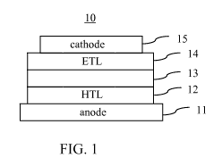
[0043] FIG. 1 shows an example of an OPV device 10 according to an
embodiment of
the present disclosure. The device 10 comprises an anode 11 (e.g. ITO), a
cathode 15, and a
photoactive region 13 disposed between the two electrodes. The OPV device 10
can further
include a charge transport layer 12, 14 disposed between the photoactive
region 13 and at
least one of the two electrodes 11, 15, where the charge transport layer
comprises a metal
oxide material doped with an organic dopant material. The charge transport
layer 12
disposed between the photoactive region 13 and the anode 11 is a HTL and the
charge
transport layer 14 disposed between the photoactive region 13 and the cathode
15 is an ETL.
The photoactive region 13 generally includes at least one organic electron
donor material and
at least one organic electron acceptor material that form a donor-acceptor
heterojunction.
Various types of donor-acceptor heterojunctions are possible as described
herein.
[0044] FIG. 2 shows another example of an OPV device 20 according to
another
embodiment. The OPV device 20 is a tandem device and can comprise an anode 21,
a
cathode 26 and multiple photoactive subcells 22, 24 provided in series between
the two
electrodes. Each of the subcells 22, 24 can comprise at least one organic
electron donor
material and at least one organic electron acceptor material that form a donor-
acceptor
heterojunction in the subcell. A thin layer of electron-hole recombination
zone 23 is
provided between the individual subcells separating the subcells. According to
the present
disclosure, the electron-hole recombination zone 23 comprises a metal oxide
material doped
with an organic dopant material. The recombination zone 23 serves to prevent
the formation
of an inverse heterojunction between the acceptor material of the anode-side
subcell and the
donor material of the cathode-side subcell. The recombination zone allows the
electrons
approaching from the anode-side subcell and the holes approaching from the
cathode-side
subcell to recombine.
9
CA 02865811 2014-08-27
WO 2013/138132
PCT/US2013/029305
[0045] Another application of the charge transport material of the present
disclosure is in
organic light emitting devices (OLEDs). In one embodiment, the metal oxide
material doped
with organic molecules can be used as one or both types of the charge
transport layers in
OLEDs. In other words, the novel charge transport material can be used for
hole transport
layers and/or electron transport layers in OLEDs.
[0046] FIG. 3 shows an example of a two-layer OLED 30 comprising an
emissive layer
32 and an electron transport layer 33 disposed in between two electrodes, an
anode 31 and a
cathode 34. According to an embodiment, the electron transport layer 33 can
comprise the
metal oxide doped with organic molecules. FIG. 4 shows an example of a three-
layer OLED
40 comprising an emissive layer 43, a hole transport layer 42, and an electron
transport layer
44 that are disposed in between an anode 41 and a cathode 44. According to
another
embodiment, one or both of the charge transport layers 44 and 42 can comprise
the metal
oxide doped with organic molecules. Various methods of fabricating OLEDs
having these
architecture are known to those skilled in the art.
[0047] Another application of the charge transport material of the present
disclosure is in
stacked light emitting devices (SOLEDs), where multiple active layers are
combined
monolithically. In SOLEDs, two or more individual emissive regions are stacked
in vertical
arrangement, the successive emissive regions being separated by an
intermediate layer. The
intermediate layers are also referred to as charge generation layers (CGLs)
because of their
charge carrier generating or injecting function in the device. A CGL is a
layer that injects
charge carriers but does not have direct external electrical connection. When
a voltage is
applied across the SOLED, the CGLs inject holes into the emissive region on
the cathode side
of the CGL, and electrons into the emissive region on the anode side of the
CGL.
[0048] FIG. 5 shows an example of a SOLED 300 having two emissive regions.
The
SOLED 300 comprises an anode 310, two organic emissive regions 320 and 330, a
CGL 350,
and a cathode 340. Organic emissive regions 320 and 330 can comprise multiple
layers, such
as hole injection layers, electron injection layers, and emissive layers. As
will be appreciated
by one skilled in the art, the emissive regions can include other layers such
as electron
blocking layers, hole blocking layer, etc. The CGL 350 is disposed between the
two emissive
regions 320 and 330. In a preferred embodiment, the CGL 350 comprises a metal
oxides
material doped with organic molecules described herein. When voltage is
applied across the
device, the CGL 350 may inject holes into the emissive region 330 and
electrons into the
CA 02865811 2014-08-27
WO 2013/138132
PCT/US2013/029305
emissive region 320. Due to the charge carrier injection properties of the CGL
350, the
device 300 may have improved efficiencies.
[0049] In one embodiment of such SOLEDs, a CGL consisting of doped
organic/Mo03
has been used by Kanno et al. (Adv. Mater. 18, 339-342 (2006)). When voltage
is applied to
the device, the CGL generates an electron on the organic side and a hole on
the Mo03 side,
which then contribute to light emission. As this process is dependent on the
availability of
free charges (Qi et al. J. Appl. Phys. 107, 014514 (2010)), it is likely that
doping the Mo03
layer with an organic molecule, thereby increasing the free charge density,
would lead to
improved performance.
[0050] In another embodiment, the OLEDs and SOLEDs described above are
phosphorescent organic light emitting devices ("PHOLED") that utilize emissive
materials
that emit light from triplet states ("phosphorescence"). But the improved
charge transport
material of the present disclosure can be applied to PHOLEDs as well as
fluorescent OLEDs.
The organic emissive materials for PHOLEDs and fluorescent OLEDs are known in
the art.
EXAMPLES
[0051] Specific representative embodiments of the invention is now
described. It is
understood that the specific methods, materials, conditions, process
parameters, apparatus
and the like are merely examples and do not necessarily limit the scope of the
invention.
Experimental Methods:
[0052] The inventors prepared and tested examples of OPV devices according
to the
following experimental procedures. Substrates consisting of indium tin oxide-
coated glass
("ITO") (150 nm, <15n, Prazisions Glas & Optik GmbH) quartz (qtz), or silicon
were
cleaned sequentially in Tergitol, deionized water, acetone, trichloroethylene,
acetone, and
isopropanol. C60 (MER, 99.9% sublimed) and AOB (Aldrich, 75%) were purified
once and
SubPc (Aldrich, 85%) was purified three times by thermal gradient sublimation
at <1x10⁻⁷
Ton-. Other materials were used as received. The ITO substrates were subjected
to a UV-
ozone treatment for 600 seconds and transferred into a nitrogen glovebox with
<0.1 ppm 02
and H20. The substrates were loaded into a high-vacuum chamber with base
pressure
<1.0x10⁻⁶ Ton-. The metal oxide host and organic dopant materials were
evaporated at 0.10
nm/s. Squaraine films were deposited from solution via spin coating in a
nitrogen
environment. All rates were measured by quartz crystal monitor and calibrated
by
spectroscopic ellipsometry.
11
CA 02865811 2014-08-27
WO 2013/138132
PCT/US2013/029305
[0053] The device performance of the sample OPV devices were measured in a
nitrogen
glovebox with <1.0 ppm 02 and <0.1 ppm H20 by an Agilent semiconductor
parameter
analyzer under illumination by a 150W Xe lamp with AM1.5G filters (Oriel).
Lamp intensity
was varied by using neutral density filters and measured using an NREL-
calibrated Si
photodiode. Incident light intensity was determined by using the spectral
correction factor,
determined from the lamp intensity and device and detector responsivities.
Experimental Results:
[0054] Single-layer "sandwich-type" devices having the structure
glass/ITO/Mo03/Au
were fabricated. The current-voltage (I- V)characteristics of these devices
were measured
and the resistivity (p=RA/t) was calculated, where R is the resistance, A is
the device area,
and t is the layer thickness, by using the Mott-Gurney relation:
R 8t3
[0055] First, the I-V characteristics of 90 nm Mo03 layers doped with
various
concentrations of AOB were measured. As shown in FIG. 6, for the neat Mo03
film, the
resistivity p was 1.6 MC2cm and decreased to below 800 kncm when the Mo03 film
was
doped with 7 vol. % AOB. Next, the absorption coefficient a of the doped metal
oxide films
was measured. As seen in FIGS. 7a and 7b, increased doping led to increased a
at longer
wavelengths. Additionally, the emergence of a new absorption peak at higher
doping
concentrations of AOB appear near 530 nm. This absorption does not correspond
to that of
neat AOB, but may reflect energy transfer from the organic dopant to the metal
oxide host.
This new absorption peak near 530 nm does not appear when doping with SubPc,
indicating
that energy transfer is not occurring.
[0056] Next, the doped Mo03 films were incorporated into sample OPV
devices. The
device structure consisted of glass/ITO/40 nm Mo03:dopant/9 nm Mo03/13 nm
SubPc/40 nm
C60/8 nm bathocuproine (BCP)/100 nm Ag. A control device with no Mo03 layers
was also
included for comparison. The dopants in these working OPV examples were AOB,
F4TCNQ
or SubPc, as compared to the control without any dopant, or the Mo03 film
doped with silver.
The 9 nm Mo03 buffer layer was incorporated into the sample devices to ensure
that the
organic dopants in the 40 nm Mo03 are not affecting Mo03/SubPC interface (e.g.
causing
exciton quenching, etc.). The inventors have found that this is not a problem.
[0057] FIGS. 8a and 8b show the dark (8a) and one-sun illuminated (8b)
plots of the J-V
characteristics of these sample OPV devices incorporating Mo03 layers doped
with Ag,
12
CA 02865811 2014-08-27
WO 2013/138132 PCT/US2013/029305
F4TCNQ, and AOB. Rs was then calculated from the dark J-V curves at forward
bias by
using a simplified version of the ideal diode equation, J = J s {exp [q(V ¨
JRs) I nkb1]¨ 1} ,
where J is the reverse saturation current, q is the electron charge, n is the
ideality factor, kb is
Boltzmann's constant, and T is absolute temperature.
[0058] Table I summarizes the results of the calculated Rs of the OPVs from
these un-
doped and doped Mo03 layers. While Rs increases from 112 1 ncm2 for undoped
case, it is
reduced to 4.3 0.1 ncm2 when doped with 1 vol.% Ag and reduced to 6.5 0.1 ncm2
when
doped with 10 vol.% AOB, which is near the value of 4.4 3 ncm2 obtained
without a Mo03
layer. Rs also decreases when F4TCNQ is used, though to a lesser degree¨this
is
unexpected, as F4TCNQ is typically used as a p-type dopant for organic
materials and Mo03
is considered by most to be an n-type material. It is possible that, because
the ionization
potential of Mo03 is larger, F4TCNQ in this case is acting as a weak n-type
dopant.
[0059] Table I. Comparison of the series resistance for OPVs with different
buffer layers.
Buffer Dopant Ratio Rs
(vol%) (nen)2)
None n/a n/a 4.4 0.3
Mo03 None 0 112 1
M003 Ag 1 4.3 0.1
M003 F4TCNQ 10 29.8 0.4
M003 AOB 10 6.51:0.1
M003 SubPc 4 70.7 0.3
[0060] Similar OPV devices were fabricated with 90 nm Mo03 layers and
varying
concentrations of AOB as the dopant. FIGS. 9a, 9b show one-sun illuminated J-V
characteristics (9a) and performance parameters (9b) of the sample OPV devices
as a
function of AOB doping concentration. As shown in FIGS. 10a, 10b, Rs decreased
from 46
ncm2 for the neat case to 8 ncm2 for 15.6 vol.% AOB.
[0061] Similar devices were also fabricated using SubPc as the dopant. In
this case, a
thick Mo03 layer was doped with 0.7 vol.% Ag, 4.0 vol.% SubPc, or undoped.
FIGS. 11a,
13
CA 02865811 2014-08-27
WO 2013/138132
PCT/US2013/029305
llb show the performance of such device. The doping with SubPc doping
increases the
device performance, compared to the undoped case.
[0062] The use of metal oxide doped with organic compounds is likely to be
beneficial in
other devices. For example, metal oxide films doped with organic molecules
could be used
for either the hole-transport layer, the electron transport layer, or both.
[0063] It may also be possible to dope oxide films which are deposited from
solution.
Although all data shown here utilizes Mo03 deposited by vacuum thermal
evaporation, it is
also possible to deposit Mo03 from solution via spincasting, spray coating,
doctor-blading, or
other techniques. Doping of oxide films deposited from solution with organic
molecules is
also possible, if a solvent is chosen which both materials are soluble in.
[0064] The foregoing description and examples have been set forth merely to
illustrate
the invention and are not intended to be limiting. Each of the disclosed
aspects and
embodiments of the present disclosure may be considered individually or in
combination with
other aspects, embodiments, and variations of the invention. In addition,
unless otherwise
specified, none of the steps of the methods of the present disclosure are
confined to any
particular order of performance. Modifications of the disclosed embodiments
incorporating
the spirit and substance of the invention may occur to persons skilled in the
art and such
modifications are within the scope of the present invention.
[0065] Those skilled in the art may appreciate that changes could be made
to the
embodiments described above without departing from the broad inventive concept
thereof It
is understood, therefore, that this invention is not limited to the particular
embodiments
disclosed, but it is intended to cover modifications within the spirit and
scope of the present
invention as defined by the attached claims.
14