Note: Descriptions are shown in the official language in which they were submitted.
CA 02866163 2014-09-02
WO 2013/142530
PCT/US2013/033023
1
METHOD AND APPARATUS FOR DISCONTINUOUS RECEPTION IN USER
EQUIPMENT FOR POWER SAVINGS
BACKGROUND
Field
[0001] Aspects of the present disclosure relate generally to wireless
communication
systems, and more particularly, to power management of a wireless device
receiver or
modem.
Background
[0002] Wireless communication networks are widely deployed to provide
various
communication services such as telephony, video, data, messaging, broadcasts,
and so
on. Such
networks, which are usually multiple access networks, support
communications for multiple users by sharing the available network resources.
One
example of such a network is the UMTS Terrestrial Radio Access Network
(UTRAN).
The UTRAN is the radio access network (RAN) defined as a part of the Universal
Mobile Telecommunications System (UMTS), a third generation (3G) mobile phone
technology supported by the 3rd Generation Partnership Project (3GPP). The
UMTS,
which is the successor to Global System for Mobile Communications (GSM)
technologies, currently supports various air interface standards, such as
Wideband-Code
Division Multiple Access (W-CDMA), Time Division¨Code Division Multiple Access
(TD-CDMA), and Time Division¨Synchronous Code Division Multiple Access (TD-
SCDMA). The UMTS also supports enhanced 30 data communications protocols, such
as High Speed Packet Access (HSPA), which provides higher data transfer speeds
and
capacity to associated UMTS networks.
[0003] As the demand for mobile broadband access continues to increase,
research and
development continue to advance the UMTS technologies not only to meet the
growing
demand for mobile broadband access, but to advance and enhance the user
experience
with mobile communications.
[0004] Furthermore, battery life has become a chief concern of
consumers wishing to
purchase a mobile device that utilizes any of the above technology types. As a
result, it
has become imperative to designers that power is conserved whenever possible
to
maximize the life of the mobile device battery. One component that may cause a
substantial drain in battery life is a mobile device receiver and its
corresponding
CA 02866163 2014-09-02
WO 2013/142530
PCT/US2013/033023
2
circuitry. Currently, many mobile device receivers provide power to all
internal
receiver components for an entire data receiving timeframe. For example, in
IJMTS, a
full receiving interval may be 20 ms for a frame. Typically, modem receiver
components are powered on throughout the entire 20 ms interval to ensure that
all
received data is able to be decoded, regardless of when in the interval the
data may be
successfully received or decoded. Therefore, typical mobile devices may
unnecessarily
use battery power when receiving a frame.
[0005] Thus, methods and apparatuses are needed to provide battery
savings for mobile
devices.
SUMMARY
[0006] The following presents a simplified summary of one or more
aspects in order to
provide a basic understanding of such aspects. This summary is not an
extensive
overview of all contemplated aspects, and is intended to neither identify key
or critical
elements of all aspects nor delineate the scope of any or all aspects. Its
sole purpose is
to present some concepts of one or more aspects in a simplified form as a
prelude to the
more detailed description that is presented later.
[0007] The present disclosure presents aspects of a method of saving
power in a
wireless device, which includes receiving data within a frame at a user
equipment (UE),
determining whether all payload packet data has been correctly decoded prior
to an end
of the frame, and powering down a receiver component for a portion of a
remainder of
the frame in response to determining that all payload packet data has been
correctly
decoded and where a first time period to a next scheduled overhead bit
transmission
period of a slot in the frame is greater than a second time period
corresponding to a
warm-up period for the receiver component.
[0008] Additionally, the present disclosure describes an apparatus for
wireless
communication, which includes means for receiving data within a frame at a
user
equipment, means for determining whether all payload packet data has been
correctly
decoded prior to an end of the frame; and means for powering down a receiver
component for a portion of a remainder of the frame in response to the means
for
determining making a determination that all payload packet data has been
correctly
decoded and where a first time period to a next scheduled overhead bit
transmission
81782221
3
period of a slot in the frame is greater than a second time period
corresponding to a warm-up
period for the receiver component.
[0009] Furthermore, the present disclosure describes a computer program
product,
including a computer-readable medium comprising code for receiving data within
a frame at a
user equipment, determining whether all payload packet data has been correctly
decoded prior
to an end of the frame, and powering down a receiver component for a portion
of a remainder
of the frame in response to determining that all payload packet data has been
correctly
decoded and where a first time period to a next scheduled overhead bit
transmission period of
a slot in the frame is greater than a second time period corresponding to a
warm-up period for
the receiver component.
[0010] Moreover, described herein is an apparatus for wireless
communication, which
includes at least one processor and a memory coupled to the at least one
processor, wherein
the at least one processor is configured to receive data within a frame at a
user equipment,
determine whether all payload packet data has been correctly decoded prior to
an end of the
frame, and power down a receiver component for a portion of a remainder of the
frame in
response to determining that all payload packet data has been correctly
decoded and where a
first time period to a next scheduled overhead bit transmission period of a
slot in the frame is
greater than a second time period corresponding to a warm-up period for the
receiver
component.
[0010a] According to one aspect of the present invention, there is provided
a method of
saving power in a wireless device, comprising: receiving data within a frame
at a user
equipment (UE); determining that the data has been correctly decoded prior to
an end of the
frame; and powering down a receiver component of the UE for a portion of a
remainder of the
frame in response to determining that the data has been correctly decoded and
upon a
determination that a first time period to a next scheduled overhead bit
transmission period of a
slot in the frame is greater than a second time period of the slot in the
frame corresponding to
a warm-up period for the receiver component.
CA 2866163 2019-05-31
81782221
3a
[0010131 According to another aspect of the present invention, there is
provided an
apparatus for wireless communication, comprising: means for receiving data
within a frame at
a user equipment (UE); means for determining that the data has been correctly
decoded prior
to an end of the frame; and means for powering down a receiver component of
the UE for a
portion of a remainder of the frame in response to the means for determining
making a
determination that the data has been correctly decoded and upon a
determination that a first
time period to a next scheduled overhead bit transmission period of a slot in
the frame is
greater than a second time period of the slot in the frame corresponding to a
warm-up period
for the receiver component.
[0010c] According to another aspect of the present invention, there is
provided a non-
transitory computer-readable medium storing instructions that when executed by
a computer
cause the computer to: receive data within a frame at a user equipment (UE);
determine that
the data has been correctly decoded prior to an end of the frame; and power
down a receiver
component of the UE for a portion of a remainder of the frame in response to
determining that
the data has been correctly decoded and upon a determination that a first time
period to a next
scheduled overhead bit transmission period of a slot in the frame is greater
than a second time
period of the slot in the frame corresponding to a warm-up period for the
receiver component.
[0010d] According to another aspect of the present invention, there is
provided an
apparatus for wireless communication, comprising: at least one processor; and
a memory
coupled to the at least one processor, wherein the at least one processor is
configured to:
receive data within a frame at a user equipment (UE); determine that the data
has been
correctly decoded prior to an end of the frame; and power down a receiver
component of the
UE for a portion of a remainder of the frame in response to determining that
the data has been
correctly decoded and upon a determination that a first time period to a next
scheduled
overhead bit transmission period of a slot in the frame is greater than a
second time period of
the slot in the frame corresponding to a warm-up period for the receiver
component.
[0011] To the accomplishment of the foregoing and related ends, the one or
more
aspects comprise the features hereinafter fully described and particularly
pointed out in the
CA 2866163 2019-05-31
81782221
3b
claims. The following description and the annexed drawings set forth in detail
certain
illustrative features of the one or more aspects. These features are
indicative, however, of but
a few of the various ways in which the principles of various aspects may be
employed, and
this description is intended to include all such aspects and their
equivalents. These and other
aspects of the invention will become more fully understood upon a review of
the detailed
description, which follows.
BRIEF DESCRIPTION OF THE DRAWINGS
[0012] FIG. 1 is a block diagram illustrating a wireless environment
according to
aspects of the present disclosure;
[0013] FIG. 2 is a flowchart illustrating aspects of a method for mobile
device battery
savings according to the present disclosure;
CA 2866163 2019-05-31
CA 02866163 2014-09-02
WO 2013/142530
PCT/US2013/033023
4
[0014] FIG. 3 is a flowchart illustrating aspects of a method for mobile
device battery
savings where a DCCII condition is encountered according to the present
disclosure;
[0015] FIG. 4 is an example waveform of a first receiver component
according to
aspects of the present disclosure;
[0016] FIG. 5 is an example waveform of a first receiver component
according to
aspects of the present disclosure;
[0017] FIG. 6 is an example waveform of a first receiver component
according to
aspects of the present disclosure;
[0018] FIG. 7 is an example waveform of a first receiver component
according to
aspects of the present disclosure;
[0019] FIG 8 is an example wavefoim of first and second receiver components
according to aspects of the present disclosure;
[0020] FIG. 9 is an example waveform of first and second receiver
components
according to aspects of the present disclosure;
[0021] FIG. 10 is an example waveform of first and second receiver
components
according to aspects of the present disclosure;
[0022] FIG. 11 is an example waveform of first and second receiver
components
according to aspects of the present disclosure;
[0023] FIG. 12 is an example waveform of first and second receiver
components
according to aspects of the present disclosure;
[0024] FIG. 13 is a block diagram of aspects of a UE device according to
aspects of the
present disclosure;
[0025] FIG. 14 is a component diagram of a logical grouping illustrating
aspects of the
present disclosure;
[0026] FIG. 15 is a block diagram illustrating an example of a hardware
implementation
for an apparatus employing a processing system;
[0027] FIG. 16 is a block diagram conceptually illustrating an example of a
telecommunications system;
[0028] FIG. 17 is a conceptual diagram illustrating an example of an access
network;
[0029] FIG. 18 is a conceptual diagram illustrating an example of a radio
protocol
architecture for the user and control plane; and
[0030] FIG. 19 is a block diagram conceptually illustrating an example of a
Node B in
communication with a UE in a telecommunications system.
CA 02866163 2014-09-02
WO 2013/142530
PCT/US2013/033023
DETAILED DESCRIPTION
[0031] The detailed description set forth below in connection with the
appended
drawings is intended as a description of various configurations and is not
intended to
represent the only configurations in which the concepts described herein may
be
practiced. The detailed description includes specific details for the purpose
of providing
a thorough understanding of various concepts. However, it will be apparent to
those
skilled in the art that these concepts may be practiced without these specific
details. In
some instances, well known structures and components are shown in block
diagram
form in order to avoid obscuring such concepts.
[0032] The present aspects relate to methods and apparatuses to power
off a modem
receiver or components of the receiver at a time prior to the end of the
frame, e.g. prior
to the end of a voice frame, such as a 20 ms frame, based on the data being
received and
properly decoded before the end of the frame. The received data packets will
often
include a Cyclic Redundancy Check (CRC), which, if it passes at the receiver,
ensures
that the data has been properly received. Therefore, in the present aspects,
if a CRC
passes "early" (e.g., at 10 ms or some other shortened interval before the end
of the
frame), which means that all data from the full frame, e.g. a 20 ms
transmission frame,
has been properly received at that "early" time, the receiver can gate off
power to one or
more receiver components for the remainder of the data transmission frame in
order to
save power in the receiver.
[0033] The receiver may also periodically wake up to receive signals
related to power
control maintenance (e.g., dedicated pilot (DP) data and transmit power
control (TPC)
data). Because the timing associated with receiving DP and TPC bits is cyclic
and
known by the receiver, the receiver can wake periodically from a powered-off
state to
receive these overhead control messages. Therefore, the present aspects
further
contemplate a method and apparatus for a receiver to periodically wake from a
powered-off state to receive the cyclic DP and TPC bits. Additionally, in
WCDMA
systems, information may be broadcast over a dedicated control channel (DCCH)
during
a longer transmission interval, such as a 40 ms interval. Aspects of the
described
apparatuses and methods may configure a receiver, or components thereof, to
accommodate the DCCH transmissions, such as by prohibiting an early power
down.
[0034] FIG.1 is a block diagram illustrating an example wireless
environment 1, which
may include one or more network entities 11 and one or more user equipment
(UE) 10,
which may be communicatively connected by one or more communication links 12.
In
CA 02866163 2014-09-02
WO 2013/142530
PCT/US2013/033023
6
an aspect, UE 10 may receive a signal 17 including data 19, such as packet
data and/or
control data, at a receiving component 14 via communication link 12 from
network
entity 11. Receiving component 14 may be configured to receive signals,
including
signal 17, from and/or send signals to network entity 11. For example,
receiving
component 14 may be configured to receive one or more data or overhead
messages
from the network entity 11. In a further aspect, receiving component 14 may be
a
component in a modem or other component in UE 10.
[0035] Furthermore, receiving component 14 may include a decoding
component 16,
which may be configured to decode one or more signals 17 from network entity
11. In
an aspect, UE 10 and network entity 11 may communicate via one or more
technologies
that specify one or more frame lengths and one or more time slots in the frame
in which
control data is to be received and decoded by decoding component 16. For
example, a
20 ms frame may be divided into a plurality of slots, which may be further
divided into
overhead data (e.g. control data) receiving intervals and packet data
receiving intervals
(e.g. package data unit (PDIT) and/or service data unit (SW) receiving
intervals). In an
aspect, overhead data may include dedicated pilot (DP) data and transmit power
control
(TPC) data. DP data may provide energy estimates used to maintain downlink
power
control to the UE 10 from the network entity 11, whereas TPC data may include
power
control bits used to maintain uplink power control from the UE 10 to the
network entity
11. In an aspect, DP data may be received in a first overhead data interval,
whereas
TPC data may be received in a separate second overhead data interval in each
slot. As
such, decoding component 16 may obtain signal 17, or a portion thereof such as
a
frame, and execute a decoding algorithm, e.g. which corresponds to an encoding
algorithm with which signal 17 was encoded, in order to obtain the data within
signal
17. Moreover, decoding component 16 may execute one or more integrity
algorithms,
such as but not limited to a cyclic redundancy check (CRC), to deteimine
whether data
19, such as all payload packet data, has been correctly decoded. In some
aspects,
decoding component 16 may complete execution of the one or more integrity
algorithms
prior to an end of the frame.
[0036] In addition, receiving component 14 may include a power
management
component 15, which may be configured to control power to one or more
components
in receiving component 14. For example, power management component 15 may
control power levels of a phase lock loop (PLL) component and corresponding
circuitry
in receiving component 14 based on an integrity state of received and decoded
signals,
CA 02866163 2014-09-02
WO 2013/142530
PCT/US2013/033023
7
such as signal 17 or a portion thereof such as a frame. For instance, in some
aspects,
power management component 15 may perform and "early." e.g. for a portion of a
remainder of the frame, power down of one or more component of receiving
component
14 in response to determining that all payload packet data has been correctly
decoded.
In an aspect, power management component 15 may perform the "early- power down
when a first time period to a next scheduled overhead bit transmission period
of a slot in
the frame is greater than a second time period corresponding to a warm-up
period for
the receiver component. Moreover, power management component 15 may take into
account waim up periods, in addition to overhead data transmission periods and
a
correct decoding determination, when determining whether to power down and/or
power up one of more components of receiver component 14.
[0037] Thus, the described apparatuses and methods, through execution
of power
management component 15, may provide UE 10 with power savings by avoiding
unnecessarily battery power usage when receiving signal 17 or a portion
thereof, such as
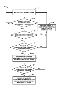
a frame. Turning to FIG. 2, illustrated are aspects of a method 2 for
maximizing battery
power in a mobile device or UE provided in the present disclosure. In an
aspect, a UE
(e.g. UE 10, FIG. 1) may receive data within a frame at block 21, wherein the
data may
be received from a network entity (e.g. network entity 11, FIG. 1). Once the
data has
been received, at block 22. the UE may determine whether all payload packet
data has
been correctly decoded at block 22. In some aspects, frame packet data may
include
packet data unit (PDU) and/or service data unit (SDU) data, which may be
distinguished
from overhead bit data and/or control data. In a further aspect, the UE may
deteimine
whether all payload packet data has been correctly decoded by determining
whether a
CRC on the received data passes, though any form of data integrity or
reliability test
may be used by the UE to determine that all payload packet data has been
correctly
received. Where not all payload packet data has been correctly decoded, the UE
may
maintain power to a receiving component to enable the UE to continue receiving
data
within the frame, for example, at block 21.
[0038] Conversely, where the UE determines that all payload packet data
has been
correctly decoded at block 22, the UE may further determine whether a DCCH
condition is present at block 23. Where a DCCH condition is present,
communication
protocols and scheduling may diverge from those typically used for packet data
transmission. For example, DCCII frames may span 40 ms, where traditional
packet
data transfer frames are 20 ms in length. Therefore, early power-down of
components
CA 02866163 2014-09-02
WO 2013/142530
PCT/US2013/033023
8
may be avoided according to aspects of the present disclosure, because to
perform early
power-down of components in a DCCII condition may lead to loss of substantial
amounts of overhead/control data. Additionally, further aspects of block 23
are
presented below in connection with FIG. 3.
[0039] Where the UE determines that a DCCH condition is present at
block 23, the UE
may maintain power to the receiver components for receipt of overhead data at
block
24. Alternatively, where the UE determines that a DCCH condition is not
present at
block 23, the UE may determine, for each receiver component, whether there is
time
available to power down the component before a required power-up period at
block 25.
In an aspect, a UE may contain one or more components that require a warm-up
period
before the components may properly receive signals and one or more components
that
require a negligible warm-up period to properly receive signals. Therefore, at
block 25,
the UE may determine, based on the warm-up period required for each receiver
component, whether each receiver component can be powered down before properly
receiving bits. In other words, where a receiver component requires a warm-up
time
greater than or equal to the length of time until the next scheduled overhead
bit
transmission time, the UE may keep the receiver component powered on to
receive
overhead data at block 24. Alternatively, where the required warm-up time is
less than
the length of time until the next scheduled overhead bit transmission time,
the UE may
power down that component for a portion of the remainder of the frame at block
26.
[0040] Furthermore, at block 27, the UE may determine for each receiver
component
whether the warm-up period required for the receiver component, which may be
substantially negligible or may be non-negligible, has arrived. Where the warm-
up
period for that receiver component has not arrived, the UE may keep the
receiver
component powered down, for example, at block 26. Alternatively, where the
warm-up
time for the receiver component has arrived at block 27, the UE may power up
the
receiver component to receive, for example, overhead bits at block 28.
Additionally, at
block 28, the UE may continue to power up the receiver component based on
scheduled
overhead bit transmission period(s) for the the remainder of the frame. As
such, UE
battery power may be conserved.
[0041] For example, one or more receiver components may demand a warm-
up period
before the components may function properly. In one aspect, such a component
may be
a phase-locked loop component, though such a component may be any receiver
component in the UE. Therefore, to allow a buffer period for such a component
to
CA 02866163 2014-09-02
WO 2013/142530
PCT/US2013/033023
9
warm up, at block 25 the UE may determine whether a first time period
corresponding
to a time period until the next scheduled overhead bit transmission period of
a slot in the
frame is greater than a second time period, which may correspond to a warm-up
period
for the receiver component. Alternatively, in some aspects, the second time
period may
correspond to substantially twice the length of the warm-up period for the
receiver
component, or any multiple of the warm-up period. By extending the second time
period to substantially twice the length of the warm-up period for the
receiver
component, the UE may be highly confident that the receiver component is fully
warmed-up and functional by the time the next scheduled overhead bit
transmission
period arrives.
[(042] When the UE executing method 2 at block 25 determines that the
second time
period is greater than or equal to the first time period, then at block 26 the
UE may
maintain power to one or more receiver components in such an instance,
depending on
factors that will be discussed below in the context of FIG. 4. For example,
the UE
executing this method may maintain power in order to avoid missing overhead
bit data
transmitted during the next scheduled overhead bit transmission period, e.g.
if the UE
were to power down a receiver component that required more warm-up time than
was
available before the next scheduled overhead bit transmission period.
[0043] When the UE executing method 2 at block 25 determines that the
first time
period is greater than the second time period, then at block 27 the UE may
power down
one or more receiver components for a portion of the remainder of the frame.
In an
aspect, such a portion of the remainder of the frame may last until the
beginning of a
required warm-up period before a next scheduled overhead bit transmission
period.
Alternatively, where one or more receiver components do not require a warm-up
period,
the portion of the remainder of the frame may last until the beginning of the
next
scheduled overhead bit period. Therefore, by powering down the one or more
receiver
components until the next scheduled overhead bit period, the UE may save
battery
power while ensuring that required overhead bits are received during scheduled
overhead bit transmission periods. Optionally, at block 28, method 2 may
continue with
additional methods, such as method 3 of Fig. 3 and/or method 5 of Fig. 5.
[(044] FIG. 3 illustrates aspects of a detailed illustration of block
23 for determining
whether a dedicated control channel (DCCH) condition is present in
methodsTuming to
FIG. 3, a scenario applicable to W-CDMA and other communication technologies
is
presented. In W-CDMA, there exist multiple types of data frames : (1) traffic
frames
CA 02866163 2014-09-02
WO 2013/142530
PCT/US2013/033023
(DTCH) and (2) overhead signaling frames (DCCH). In WCDMA, there is no way to
know whether a particular received transmission is traffic or overhead
signaling data.
Adding a further complication, DCCH is transmitted over a 40 ms frame instead
of a 20
ms frame. Therefore, if the receiver or one or more receiver components are
powered
off after a shortened interval prior to the end of a frame (e.g. a 10 ms
interval) there is
only 25% reliability that all of the DCCH bits have been received.
[0045] Furthermore, DCCH signaling data has no packet indicator bits,
unlike
traditional data bits, which may include Cyclic Redundancy Check (CRC) bits.
In some
instances, however, the DTCH traffic bits may include CRC bits and the DTCH
bits
may be broadcast with the DCCH bits as multicast traffic. In such a situation,
in some
described aspects, the receiver may assume that the DCCII bits are correctly
received if
the DTCH CRC passes. Thus, early receiver power off can be performed with this
assumption.
[0046] Alternatively or additionally, detection of DCCH traffic can be
performed based
on thresholding. Using this method, if a threshold energy value related to the
DCCH
during an interval is not reached, then the absence of DCCH during that
interval can be
assumed and the receiver may power down for the remainder of the frame with
some
confidence that DCCH data is not being missed. For example, the receiver may
use an
accumulated DP and TPC energy within a shortened subfi-ame (e.g. a 10 ms
subframe)
as a reference energy level. In block 23 of FIG. 2, if an accumulated DCCH
energy
level over this same time period is lower than this reference energy level by
a particular
threshold value, then an absence of DCCH data can be declared and the receiver
may
power down completely or may power down some of its components.
[(047] Specifically, turning to block 51, a UE may obtain a threshold
DCCII energy
value. In an aspect, the UE may obtain this threshold DCCH energy value from a
network component in a transmission or may obtain the value from pre-
configured
memory on the UE. Alternatively or additionally, a user or network
administrator may
set the threshold DCCH value in, for example, a user interface on the UE.
Furthermore,
in an aspect, the threshold DCCH energy value may correspond to an accumulated
dedicated pilot (DP) data and transmit power control (TPC) data energy
received within
a reference frame sub-period, which, for example, may be a 10 ms time period.
Additionally, at block 52, the UE may compute an accumulated DCCH energy value
that has been received by the UE in the frame over a sampling time interval.
Next, at
block 53, the UE may compare the accumulated DCCH energy value to the
threshold
CA 02866163 2014-09-02
WO 2013/142530
PCT/US2013/033023
11
DCCH energy value. Where the accumulated DCCH energy value is lower than the
threshold DCCII energy value, then the absence of a DCCII may be declared at
block
54. Alternatively or additionally, the comparing may take into account a
buffer
threshold below the DCCH energy threshold. In such an aspect, where the
accumulated
energy is lower than the threshold DCCH energy value by at least the buffer
threshold,
the absence of DCCH can be declared as in block 54. Thus, by implementing the
buffer
threshold, the UE may declare the absence of a DCCH with greater confidence.
[(048] In a further aspect, at block 55, where the accumulated DCCH energy
value is
greater than or equal to the DCCH energy threshold (or the threshold minus the
buffer
threshold as above), the UE may declare the presence of a DCCH and/or
communication according to a DCCII standard (e.g. 40 ms frame length) at block
55
[(049] In another aspect of the present invention, data that is comprised
of more than
one type or class of frame may be communicated to the UE 10, which may base a
decision to power down one or more receiver components receiving all classes
of data
based on correct receipt of one of the classes. For example, in a specific
example of this
aspect, the data transmitted is comprised of voice data coded to correspond
with the
Adaptive Multi-Rate (AMR) 12.2k coding standard. The voice data in AMR 12.2k
is
sent to the physical layer in three classes: A, B, and C. where each class has
a specified
level of required reliability. Each class of data may be sent in different
streams because
they may individually tolerate different error rates. In AMR 12.2k voice data,
for
example, CRC data is only added to class A data. In the present aspect, the
receiver
may assume that the class B and/or class C data has been correctly received if
the CRC
associated with the frame's class A data passes, for example, at block 22 of
FIG. 2.
Therefore, if the CRC or the class A passes in a shorter interval than the
typical 20 ms
frame (e.g., a 10 ms shortened interval), the receiver may choose to power
down all or
some of its components for the remainder of the frame to save power.
Alternatively, the
AMR 12.2 data may be comprised of full rate, SID, and null rate frames. Also
applicable are AMR 7.9 kbps and AMR 5.9 kbps standards for UMTS.
[0050] 'l'o further illustrate aspects of the present disclosure, FIGS.
4-12 present
waveform diagrams according to aspects of methods described herein, such as,
but not
limited to the methods described in relation to FIGS. 2 AND 3. Each of the
FIGS. 6-14
include a frame schedule according to two example slots in an example data
transmission frame, which are indicated above the frame schedule. The frame
schedule
delineates several sub-periods in each slot, which, in the example slots (slot
1 and slot
81782221
12
2) include a first overhead bit transmission sub-period OH 1, a first data
transmission sub-period
DATA 1, a second overhead bit transmission sub-period OH 2, and a second data
transmission sub-
period DATA 2. In an aspect, control data, such as dedicated pilot (DP)
information and transmit
power control (TPC) information may be transmitted and/or received or may be
scheduled to be
transmitted and/or received during one or both of OH 1 and OH 2.
[0051] Additionally illustrated in FIGS. 4-12 are power waveforms
representing a power on
state or a power off state of one or more receiver components, such as, but
not limited a first receiver
component (Component 1), which may have a warm-up period, and a second
receiver component
(Component 2), which may have essentially no warm-up period, e.g. a warm-up
period equal to zero
or a substantially negligible value. In some aspects, a non-zero warm-up
required component may
correspond to a phase-locked loop component, which may have one or multiple
operational warm-up
periods (represented as WU) before overhead bit transmission periods.
Additionally, in some aspects,
the non-non-zero warm-up-required component may be a receiver component that
does not require a
warm-up period. Further, in FIGS. 4-12, time increases along the horizontal
axis of each frame and
each corresponding power waveform.
[0052] Furthermore, the operation corresponding to the power waveforms in
FIGS. 4-12 is
based on several key assumptions. For example, negligible convolutional
decoder delay is assumed, as
is negligible warm-up time for automatic gain control (AGC) circuits or
components and negligible
group delay for an optional rake receiver. In some aspects, because a phase-
locked loop component
may remain on during a power-down interval, no warm-up time may be assumed
during or following
such an interval.
[0053] Turning to FIG. 4, an example of an operational scenario 600
includes a power
waveform diagram 602 that illustrates an example operation of a first receiver
component, component
1, relative to a frame 604 having frame schedule 606. Operational scenario 600
may include, but is not
limited to aspects of method 2 (FIG. 2). Furthermore, levels 608 and 610
represent voltage levels
corresponding to On and OFF positions, respectively. For example, at point 612
in sub-period DATA
1, the UE may determine that all payload packet data, which may include all
PDU or SDU data but
may not include control or overhead data, has been correctly received and
decoded (e.g. CRC passes),
as in block 22 (FIG. 2), and that the frame is not yet completed, as in block
23 (FIG. 2). Additionally,
because the time 618 before the next scheduled overhead bit transmission
period, OH 2, is greater than
the warm-up period 620 for Component 1, the HE may power down the receiver
component until the
warm-up period commences at point 614
CA 2866163 2019-05-31
81782221
13
(e.g block 27, FIG. 2). Additionally, because the next warm-up period has
arrived at point 614, the
UE may again power up Component 1. Thereafter, the UE may power down Component
1 after each
scheduled overhead bit transmission period because all of the frame data has
been correctly received
after point 612. Such operation may continue in the same manner with respect
to each OH period in
the frame and/or subsequent frames.
[0054] Turning to FIG. 5, another example of an operational scenario 700
includes a power
waveform diagram 702 that illustrates an example operation of a first receiver
component, Component
1, relative to a frame 704 having frame schedule 706 according to aspects of
the present disclosure.
Furthermore, levels 708 and 710 represent voltage levels corresponding to On
and OFF positions,
respectively. Furthermore, optional scenario 700 includes first time period
718 corresponding to the
time until the next scheduled overhead bit transmission period and second time
period 720
corresponding to the warm-up period of Component 1. In some aspects, after
correct receipt and
decoding of all payload packet data, LIE may keep Component 1 powered on from
the beginning of
WU to the receipt of all overhead data in a slot, but may power Component 1
down thereafter. At
point 712, for example, the HE may determine that all payload packet data has
been correctly received
and decoded, but may not power down Component 1 at point 714 because, in this
example, the UE
will receive all overhead data within the slot before powering down.
Therefore, the UE may keep
Component I powered up until point 716, where the UE will power down Component
1 until a warm-
up period WU anticipating overhead data transmission in a new slot (slot 2).
Thus, through
maintaining power to Component 1 until all overhead data has been received,
the UE may minimize
the potential for losing overhead data essential for proper control of UE
communication with a
network. It is also understood that, although the waveforms of FIGS. 4-12 show
the UE powering
down Component I at the moment that all payload packet data is correctly
received (see, e.g., points
916, 1024, 1122, 1224, and/or 1424), the UE may alternatively control power to
Component 1 to
conform to the waveform of FIG. 7 to ensure complete reception of all overhead
bits in a slot.
[0055] Turning to FIG. 6, another example of an operational scenario 800
includes a power
waveform diagram 802 that illustrates an example operation of a first receiver
component, Component
1, relative to a frame 804 having frame schedule 806 according to aspects of
the present disclosure.
Furthermore, levels 808 and 810 represent voltage levels corresponding to ON
and OFF positions,
respectively. Furthermore, optional scenario 800 includes first time period
818 corresponding to the
time until the next
CA 2866163 2019-05-31
CA 02866163 2014-09-02
WO 2013/142530
PCT/US2013/033023
14
scheduled overhead bit transmission period and second time period 820
corresponding
to the warm-up period of Component 1. FIG. 6 illustrates an example operation
of a
non-zero warm-up-required component according to aspects of the present
disclosure,
which may include, but is not limited to aspects of method 2 (FIG. 2). For
example, the
UE may determine at point 812 that all payload packet data has been correctly
received
and decoded (e.g. CRC passes), as in block 22 (FIG. 2), and that the frame is
not yet
completed, as in block 23 (FIG. 2). Additionally, the UE may maintain power to
Component 1 for receipt of overhead bits during OH 2. Additionally, because
all
payload packet data has been received as of point 812, the UE may power down
Component 1 at point 814 without risking the loss of frame data.
[0056] Additionally, turning to FIG. 7, another example of an
operational scenario 900
includes a power waveform diagram 902 that illustrates an example operation of
a first
receiver component, Component 1, relative to a frame 904 having frame schedule
906
according to aspects of the present disclosure. Furthermore, optional scenario
900
includes first time period 918 corresponding to the time until the next
scheduled
overhead bit transmission period and second time period 920 corresponding to
twice the
required component warm-up time period. In addition, levels 908 and 910
represent
voltage levels corresponding to ON and OFF positions, respectively. Waveform
902 is
example waveform for an example operation where warm-up period for Component 1
is
optionally equal to twice the traditional required warm-up period for the
component
For example, the UE may determine at point 912 that all payload packet data
has been
correctly received and decoded (e.g. CRC passes), as in block 22 (FIG. 2).
Additionally, the UE may determine that the time period 918 until the next
scheduled
overhead bit transmission (OH 2) is not greater than twice warm-up period 920
for
Component 1 (WU), which begins at point 914. Therefore, there is not time to
power
down Component 1. Furthermore, though FIG. 7 depicts an example waveform where
the second time period 920 is equal to twice the typical warm-up period of
Component
1, any multiple of the typical warm-up period may be utilized as the warm-up
period,
including time periods that are not multiples of the traditional required warm-
up period.
As such, because the UE may maintain power to Component 1 for receipt of
overhead
bits during OH 2. Additionally, because all payload packet data has been
received as of
point 912, the UE may power down Component 1 at point after OH 2 of slot 1
without
risking the loss of frame data.
CA 02866163 2014-09-02
WO 2013/142530
PCT/1JS2013/033023
[0057] Turning to
FIG. 8, another example of an operational scenario 1000 includes
power waveform diagrams 1002 and 1004 that illustrate example operation of a
first
receiver component, Component 1 and a second receiver component. Component 2,
respectively, relative to a frame 1006 having frame schedule 1008 according to
aspects
of the present disclosure. Furthermore, optional scenario 1000 includes first
time period
1026 corresponding to the time until the next scheduled overhead bit
transmission
period and second time period 1028 corresponding to the warm-up period of
Component 1. In addition, levels 1010 and 1014 represent ON voltage levels
corresponding, whereas levels 1012 and 1016 represent OFF positions. According
to
aspects of FIG. 8, an Component 1 may require a non-negligible warm-up time
(WU)
and Component 2 may have a substantially negligible warm-up time., and
operation
thereof may include, but is not limited to, aspects of methods 2 and/or 3
(FIGS. 2 and
3). For example, at point 1018, in sub-period DATA 1, the UE may determine
that all
payload packet data has been correctly received and decoded (e.g. CRC passes),
as in
block 22 (FIG. 2), and that the frame is not yet completed, as in block 23
(FIG. 2).
Additionally, because the time 1026 until the next scheduled overhead bit
transmission
period, OH 2, is greater than the warm-up period 1028 for Component 1, the UE
may
power down Component 1 and Component 2 at point 1018 as at block 27 (FIG. 2).
Furthermore, at point 1020, as the beginning of the warm-up period has arrived
and the
receiver has one or more non-zero warm-up-required component the UE may power
up
Component 1. Component 2, however, may remain powered off until point 1022 at
the
start of OH 2, which is the next overhead bit transmission period.
[0058] Turning to FIG. 9, another example of an operational scenario
1100 includes
power waveform diagrams 1102 and 1104 that illustrate example operation of a
first
receiver component, Component 1 and a second receiver component. Component 2,
respectively, relative to a frame 1106 having frame schedule 1108 according to
aspects
of the present disclosure. Furthermore, optional scenario 1100 includes first
time period
1124 corresponding to the time until the next scheduled overhead bit
transmission
period and second time period 1126 corresponding to the warm-up period of
Component 1. Additionally, levels 1110 and 1114 represent ON voltage levels
corresponding, whereas levels 1112 and 1116 represent OFF positions.
[0059] In an aspect, at point 1118 in sub-period DATA 1, the UE may
determine that all
payload packet data has been correctly received and decoded (e.g. CRC passes),
as in
block 22 (FIG. 2). Additionally, because at point 1118 the time period 1126
CA 02866163 2014-09-02
WO 2013/142530
PCT/US2013/033023
16
corresponding to the warm-up period is longer than the time period 1124 to the
start of
the next scheduled overhead bit transmission period, OH 2, the IT may maintain
power
to Component 1 for receipt of the overhead bits. Additionally, because the
next
scheduled overhead bit period does not begin until point 1120, the UE may
power down
Component 2 at point 1118. Furthetinore, at point 1120, the UE may further
power up
Component 2 at point 1120 as in block 46 of FIG. 47. As such, the LIE may save
power
without risk of missing needed data by powering off Component 2 from point
1118 to
point 1120, as all payload packet data has been correctly decoded by point
1118.
[0060] Turning to FIG. 10, another example of an operational scenario
1200 includes
power waveform diagrams 1202 and 1204 that illustrate example operation of a
first
receiver component, Component 1 and a second receiver component, Component 2,
respectively, relative to a frame 1206 having frame schedule 1208 according to
aspects
of the present disclosure. Furthermore, optional scenario 1200 includes first
time period
1226 corresponding to the time until the next scheduled overhead bit
transmission
period and second time period 1228 corresponding to the traditional warm-up
period of
Component 1. In addition, levels 1210 and 1214 represent ON voltage levels
corresponding, whereas levels 1212 and 1216 represent OFF positions. According
to
aspects of FIG. 10, Component 1 may require a non-negligible wamt-up time (WU)
and
Component 2 may have a substantially negligible warm-up time. The waveform of
FIG. 10 illustrates an example method wherein the LIE maintains power to
Component 2
during scheduled overhead bit transmission periods of every nth slot of a
frame. For
example, in FIG. 10, the wavefoim may illustrate an example waveform wherein n
equals 2, meaning that the UE powers up Component 2 during OH 1 and OH 2 of
every
other slot. In an example, such a method may be implemented where channel,
link,
and/or network conditions are particularly reliable. Thus, maintaining power
to one
component every n slots may save battery power with a relatively low risk of
missing
overhead data. as Component 1 may continue to receive power during OH 1 and OH
2
of every slot.
[0061] With specific reference to FIG. 10, at point 1218, in sub-period
DATA 1, the UE
may determine that all payload packet data has been correctly received and
decoded
(e.g. CRC passes), as in block 22 (FIG. 2), and that the frame is not yet
completed, as in
block 23 (FIG. 2). As a result, the UE may power off Component 1 and Component
2
at point 1218 because there exists time to power down the components before
the warm-
up or next scheduled overhead bit transmission period. Additionally, at point
1220, the
CA 02866163 2014-09-02
WO 2013/142530
PCT/US2013/033023
17
UE may power off both Component 1 and Component 2 because OH 2 has finished
and
all payload packet data has been received as of point 1218. However, after
point 1220,
though the waveform of Component 1 may behave according to previous aspects,
Component 2 may not be powered on for the remainder of slot 2. For example,
whereas
in other aspects the UE may power up Component 2 at point 1222, the UE may, in
an
aspect, detect relatively strong network conditions and not power on Component
2 until,
for example slot 3 where n = 2, slot 4 where n=3, and so on. In an aspect, n
may be a
positive integer and/or a fraction of a positive integer, for example, or may
be
represented by a decimal number. Furthermore, in an additional example,
Component 2
may behave according to previous aspects, whereas the UE may power down
Component 1 during every II slots. Thus, additional power savings may be
realized
where a UE powers on a component for overhead data reception for only every n
slots.
[0062] Turning to FIG. 11, another example of an operational scenario
1300 includes
power waveform diagrams 1302 and 1304 that illustrate example operation of a
first
receiver component, Component 1 and a second receiver component, Component 2,
respectively, relative to a frame 1306 having frame schedule 1308 according to
aspects
of the present disclosure. Furthermore, levels 1310 and 1314 represent ON
voltage
levels corresponding, whereas levels 1312 and 1316 represent OFF positions.
According to aspects of FIG. 11, Component 1 may require a non-negligible warm-
up
time (W U) and Component 2 may have a substantially negligible warm-up time.
In an
aspect, the UE may power up both Component 1 and Component 2 during every n
slots.
For example, at point 1318, the UE may determine that all payload packet data
has been
correctly decoded, and may power down both Component 1 and Component 2 until
the
beginning of a warm-up period and a scheduled overhead bit data period OII 2,
respectively. However, after point 1320, the UE may power down both Component
1
and Component 2 during the remainder of slot 1 and for the entirety of the
subsequent
slot, slot 2. In an aspect, the operation of FIG. 11 may be utilized in
relatively strong
network conditions where the UE determines that sufficient overhead data may
be
obtained when receiving such overhead data via Component 1 and Component 2
during
every n frames. Thus, in such conditions, additional power savings may be
realized by
powering down a plurality of components every n slots in a frame.
[0063] Turning to FIG. 12, another example of an operational scenario
1400 includes
power waveform diagrams 1402 and 1404 that illustrate example operation of a
first
receiver component, Component 1 and a second receiver component, Component 2,
81782221
18
respectively, relative to a frame 1406 having frame schedule 1408 according to
aspects of the
present disclosure.
Furthermore, levels 1410 and 1414 represent ON voltage levels
corresponding, whereas levels 1412 and 1416 represent OFF positions. According
to aspects of
FIG. 12, Component 1 may require a non-negligible warm-up time (WU) and
Component 2 may
have a substantially negligible warm-up time. For example, in FIG. 12, a UE
may power on a
second component before the beginning of one or more scheduled overhead bit
transmission
periods to ensure that the second component is powered on for the entirety of
the scheduled
overhead bit transmission periods. Specifically, at point 1418, for example,
the UE may
determine that all payload packet data has been correctly received and
decoded, and therefore may
power down both Component 1 and Component 2. Turning to Component 2, whereas
the UE in
methods described above may have waited to power up Component 2 at point 612C
corresponding
to the beginning of OH 2 1422, in the method of FIG. 12, the UE may power
Component 2 at an
earlier point, such as point 1420. By doing so, the UE may further ensure that
all overhead data is
received during OH 2 and subsequent overhead transmission periods in the frame
while saving
power, for example, by powering down Component 2 between point 1418 and point
1420.
[0064]
Referring to FIG. 13, in one aspect, UE 10 (FIG. 1) is represented. UE 10
includes a processor 1500 for carrying out processing functions associated
with one or more of
components and functions described herein. Processor 1500 can include a single
or multiple set of
processors or multi-core processors. Moreover, processor 1500 can be
implemented as an
integrated processing system and/or a distributed processing system.
[0065] UE 10
further includes a memory 1502, such as for storing data used herein and/or
local versions of applications being executed by processor 1500. Memory 1502
can include any
type of memory usable by a computer, such as random access memory (RAM), read
only memory
(ROM), tapes, magnetic discs, optical discs, volatile memory, non-volatile
memory, and any
combination thereof.
[0066]
Additionally, UE 10 may further include a data store 1504, which can be any
suitable combination of hardware and/or software, that provides for mass
storage of information,
databases, and programs employed in connection with aspects described herein.
For example,
data store 1504 may be a data repository for applications not currently being
executed by
processor 1500.
CA 2866163 2019-05-31
CA 02866163 2014-09-02
WO 2013/142530
PCT/US2013/033023
19
[0067] UE 10 may
additionally include a user interface component 1506 operable to
receive inputs from a user of UE 10, and further operable to generate outputs
for
presentation to the user. User interface component 1506 may include one or
more input
devices, including but not limited to a keyboard, a number pad, a mouse, a
touch-
sensitive display, a navigation key, a function key, a microphone, a voice
recognition
component, any other mechanism capable of receiving an input from a user, or
any
combination thereof. Further, user interface component 1506 may include one or
more
output devices, including but not limited to a display, a speaker, a haptic
feedback
mechanism, a printer, any other mechanism capable of presenting an output to a
user, or
any combination thereof.
[0068] Further, UE 10 includes a communications component 1507 that
provides for
establishing and maintaining communications with one or more parties utilizing
hardware, software, and services as described herein. Communications component
1507 may carry communications between components on UE 10, as well as between
UE
and external devices, such as devices located across a communications network
and/or devices serially or locally connected to UE 10, for example, network
entity 11
(FIG. 1). For example, UE 10 may include one or more buses, and may further
include
transmit chain components and receive chain components associated with a
transmitter
and receiver, respectively, operable for interfacing with external devices.
[0069] Additionally, UE 10 may include a receiving component 14 that
may receive one
or more signals containing data, such as frame data and/or overhead or control
data
from, for example, a network entity 11. In some aspects, receiving component
14 may
be configured to perform some or all of the method steps of the methods
corresponding
to FIGS. 2 AND 3. In a further aspect, receiving component 14 may be a
receiver,
transceiver, or any other electrical component and/or circuitry capable of
receiving
and/or processing electromagnetic signals.
[0070] Furthermore, receiving component 14 may contain power management
component 15 configured to manage power to one or more receiver components.
Power
management component may contain a data class manager 1508, which may be
configured to recognize the receipt of certain classes of data and base a
decision to
power up or power down one or more receiver components based on the correct
receipt
of one or more classes of data in a frame. In an aspect, such classes of data
may include
classes A, B, and C data of AMR 12.2k standard voice data.
CA 02866163 2014-09-02
WO 2013/142530
PCT/US2013/033023
[0071]
Additionally, power management component 15 may include a warm-up period
manager 1510, which may be configured to store information pertaining to the
required
warm-up periods of one or more receiver components in UE 10. Also, power
management component 15 may contain a transmission schedule maintaining
component 1512, which may be configured to receive and/or store a transmission
schedule for a particular communication standard, such as a communication
standard
being utilized for communication with one or more network entities 11.
Furthermore,
power management component 15 may include a DCCH management component 1514
configured to determine whether a DCCH condition is present. For example, in
some
aspects, DCCH management component 1514 may determine a threshold DCCH energy
value and/or an accumulated DCCII energy value. In addition, DCCII management
component 1514 may compare the threshold DCCH energy value to the accumulated
DCCH energy value and make a determination regarding the presence of a DCCH
therefrom. In an additional aspect, receiving component 14 may include a
decoding
component 16 for decoding received data, such as frame data (e.g. PDIT and/or
SUIT
data) and overhead or control data.
[(072] Referring to FIG. 14, an example system 1600 is displayed for
selectively
powering on and powering off one or more receiver components for UE power
savings.
For example, system 1600 can reside at least partially within a device, such
as UE 10. It
is to be appreciated that system 1600 is represented as including functional
blocks,
which can be functional blocks that represent functions implemented by a
processor,
software, or combination thereof (e.g., firmware). System 1600 includes a
logical
grouping 1602 of electrical components that can act in conjunction. For
example,
logical grouping 1602 can include an electrical component 1604 for receiving
data from
a network entity. In an example, electrical component 1604 may be receiving
component 14 (FIGS. 1 and 15), and may be configured to receive frame data
(e.g. PDU
and/or SDU data) and overhead or control data. Additionally, logical grouping
1602
can include an electrical component 1606 for switching power on or off to one
or more
receiver components. In an example, electrical component 1606 may be power
management component 15 (FIGS. 1 and 15). Furtheimore, logical grouping 1602
can
include an electrical component 1608 for decoding received data. In an
example,
electrical component 1606 may be decoding component 16 (FIGS. 1 and 15).
Optionally, in an additional aspect, logical grouping 1602 can include an
electrical
component 1610 for detecting and/or managing the presence of a DCCH. In an
CA 02866163 2014-09-02
WO 2013/142530
PCT/US2013/033023
21
example, electrical component 1610 may be DCCH management component 1514 (FIG.
13). In a further optional aspect, where a DCCII is present, DCCII management
component 1514 may cancel any potential early power-off of receiver
components.
[0073] Additionally, system 1600 can include a memory 1612 that retains
instructions
for executing functions associated with the electrical components 1604, 1606,
1608, and
1610, stores data used or obtained by the electrical components 1604, 1606,
1608, and
1610, etc. While shown as being external to memory 1612, it is to be
understood that
one or more of the electrical components 1604, 1606, 1608, and 1610 can exist
within
memory 1612. In one example, electrical components 1604, 1606, 1608, and 1610
can
comprise at least one processor, or each electrical component 1604, 1606,
1608, and
1610 can be a corresponding module of at least one processor. Moreover, in an
additional or alternative example, electrical components 1604, 1606, 1608, and
1610
can be a computer program product including a computer readable medium, where
each
electrical component 1604, 1606, 1608, and 1610 can be corresponding code.
[0074] FIG. 15 is a block diagram illustrating an example of a hardware
implementation for an apparatus 100 employing a processing system 114. In an
aspect,
apparatus 100 and/or processing system 114 may include receiving component 14
(FIGS. 1 and 15) and/or power management component 15 (FIGS. 1 and 15). In
this
example, the processing system 114 may be implemented with a bus architecture,
represented generally by the bus 102. 'The bus 102 may include any number of
interconnecting buses and bridges depending on the specific application of the
processing system 114 and the overall design constraints. The bus 102 links
together
various circuits including one or more processors, represented generally by
the
processor 104, and computer-readable media, represented generally by the
computer-
readable medium 106. The bus 102 may also link various other circuits such as
timing
sources, peripherals, voltage regulators, and power management circuits, which
are well
known in the art, and therefore, will not be described any further. A bus
interface 108
provides an interface between the bus 102 and a transceiver 110. The
transceiver 110
provides a means for communicating with various other apparatus over a
transmission
medium. Depending upon the nature of the apparatus, a user interface 112
(e.g.,
keypad, display, speaker, microphone, joystick) may also be provided.
[0075] The processor 104 is responsible for managing the bus 102 and
general
processing, including the execution of software stored on the computer-
readable
medium 106. The software, when executed by the processor 104, causes the
processing
81782221
22
system 114 to perform the various functions described infra for any particular
apparatus. The
computer-readable medium 106 may also be used for storing data that is
manipulated by the processor
104 when executing software.
[0076] The various concepts presented throughout this disclosure may be
implemented across
a broad variety of telecommunication systems, network architectures, and
communication standards.
By way of example and without limitation, the aspects of the present
disclosure illustrated in FIG. 16
are presented with reference to a UNITS system 200 employing a W-CDMA air
interface. UMTS
system 200 may, for example, be wireless environment 1 of FIG. 1, and may
include one or more
network entities 11 (FIG. 1) and/or one or more UEs 10 (FIG. 1), which may
perform one or more of
the methods for optimizing battery power as illustrated in FIGS. 2 AND 3. A
UMTS network includes
three interacting domains: a Core Network (CN) 204, a UMTS Terrestrial Radio
Access Network
(UTRAN) 202, and User Equipment (UE) 210. In this example, the UTRAN 202
provides various
wireless services including telephony, video, data, messaging, broadcasts,
and/or other services. The
UTRAN 202 may include a plurality of Radio Network Subsystems (RNSs) such as
an RNS 207, each
controlled by a respective Radio Network Controller (RNC) such as an RNC 206.
Here, the UTRAN
202 may include any number of RNCs 206 and RNSs 207 in addition to the RNCs
206 and RNSs 207
illustrated herein. The RNC 206 is an apparatus responsible for, among other
things, assigning,
reconfiguring and releasing radio resources within the RNS 207. The RNC 206
may be interconnected
to other RNCs (not shown) in the UTRAN 202 through various types of interfaces
such as a direct
physical connection, a virtual network, or the like, using any suitable
transport network.
[0078] Communication between a UE 210 and a Node B 208 may be considered as
including
a physical (PHY) layer and a medium access control (MAC) layer. Further,
communication between a
UE 210 and an RNC 206 by way of a respective Node B 208 may be considered as
including a radio
resource control (RRC) layer. In the instant specification, the PHY layer may
be considered layer 1;
the MAC layer may be considered layer 2; and the RRC layer may be considered
layer 3. Information
hereinbelow utilizes terminology introduced in the RRC Protocol Specification,
3GPP TS 25.331 v
9.1Ø
100781 The geographic region covered by the RNS 207 may be divided into a
number of
cells, with a radio transceiver apparatus serving each cell. A radio
transceiver apparatus is commonly
referred to as a Node B in UMTS applications, but may also be referred to
CA 2866163 2019-05-31
CA 02866163 2014-09-02
WO 2013/142530
PCT/US2013/033023
23
by those skilled in the art as a base station (BS), a base transceiver station
(BTS), a
radio base station, a radio transceiver, a transceiver function, a basic
service set (BSS),
an extended service set (ESS), an access point (AP), or some other suitable
terminology.
For clarity, three Node Bs 208 are shown in each RNS 207; however, the RNSs
207
may include any number of wireless Node Bs. The Node Bs 208 provide wireless
access points to a CN 204 for any number of mobile apparatuses. Examples of a
mobile
apparatus include a cellular phone, a smart phone, a session initiation
protocol (SIP)
phone, a laptop, a notebook, a netbook, a smartbook, a personal digital
assistant (PDA),
a satellite radio, a global positioning system (GPS) device, a multimedia
device, a video
device, a digital audio player (e.g., MP3 player), a camera, a game console,
or any other
similar functioning device. The mobile apparatus is commonly referred to as a
UE in
UMTS applications, but may also be referred to by those skilled in the art as
a mobile
station, a subscriber station, a mobile unit, a subscriber unit, a wireless
unit, a remote
unit, a mobile device, a wireless device, a wireless communications device, a
remote
device, a mobile subscriber station, an access terminal, a mobile terminal, a
wireless
terminal, a remote teiminal, a handset, a temtinal, a user agent, a mobile
client, a client,
or some other suitable terminology. In a UMTS system, the UE 210 may further
include a universal subscriber identity module (USIM) 211, which contains a
user's
subscription information to a network. For illustrative purposes, one UE 210
is shown
in communication with a number of the Node Bs 208. The DL, also called the
forward
link, refers to the communication link from a Node B 208 to a UE 210, and the
UL, also
called the reverse link, refers to the communication link from a UE 210 to a
Node B
208.
[0079] The CN 204 interfaces with one or more access networks, such as
the UTRAN
202. As shown, the CN 204 is a GSM core network. However, as those skilled in
the
art will recognize, the various concepts presented throughout this disclosure
may be
implemented in a RAN, or other suitable access network, to provide UEs with
access to
types of CNs other than GSM networks.
[0080] The CN 204 includes a circuit-switched (CS) domain and a packet-
switched
(PS) domain. Some of the circuit-switched elements are a Mobile services
Switching
Centre (MSC), a Visitor location register (VLR) and a Gateway MSC. Packet-
switched
elements include a Serving GPRS Support Node (SGSN) and a Gateway GPRS Support
Node (GGSN). Some network elements, like EIR, IILR, VLR and AuC may be shared
by both of the circuit-switched and packet-switched domains. In the
illustrated
CA 02866163 2014-09-02
WO 2013/142530
PCT/US2013/033023
24
example, the CN 204 supports circuit-switched services with a MSC 212 and a
GMSC
214. In some applications, the GMSC 214 may be referred to as a media gateway
(MGW). One or more RNCs, such as the RNC 206, may be connected to the MSC 212.
The MSC 212 is an apparatus that controls call setup, call routing, and UE
mobility
functions. The MSC 212 also includes a VLR that contains subscriber-related
information for the duration that a UE is in the coverage area of the MSC 212.
The
GMSC 214 provides a gateway through the MSC 212 for the LIE to access a
circuit-
switched network 216. The GMSC 214 includes a home location register (HLR) 215
containing subscriber data, such as the data reflecting the details of the
services to which
a particular user has subscribed. The HLR is also associated with an
authentication
center (AuC) that contains subscriber-specific authentication data. When a
call is
received for a particular UE, the GMSC 214 queries the HLR 215 to determine
the UE' s
location and forwards the call to the particular MSC serving that location.
[(081] The CN 204 also supports packet-data services with a serving GPRS
support
node (SGSN) 218 and a gateway GPRS support node (GGSN) 220. GPRS, which
stands for General Packet Radio Service, is designed to provide packet-data
services at
speeds higher than those available with standard circuit-switched data
services. The
GGSN 220 provides a connection for the UTRAN 202 to a packet-based network
222.
The packet-based network 222 may be the Internet, a private data network, or
some
other suitable packet-based network. The primary function of the GGSN 220 is
to
provide the UEs 210 with packet-based network connectivity. Data packets may
be
transferred between the GGSN 220 and the UEs 210 through the SGSN 218, which
performs primarily the same functions in the packet-based domain as the MSC
212
performs in the circuit-switched domain.
[(082] An air interface for UMTS may utilize a spread spectrum Direct-
Sequence Code
Division Multiple Access (DS-CDMA) system. The spread spectrum DS-CDMA
spreads user data through multiplication by a sequence of pseudorandom bits
called
chips. The "wideband" W-CDMA air interface for UMTS is based on such direct
sequence spread spectrum technology and additionally calls for a frequency
division
duplexing (FDD). FDD uses a different carrier frequency for the UL and DL
between a
Node B 208 and a UE 210. Another air interface for UMTS that utilizes DS-CDMA,
and uses time division duplexing (TDD), is the TD-SCDMA air interface. Those
skilled
in the art will recognize that although various examples described herein may
refer to a
CA 02866163 2014-09-02
WO 2013/142530
PCT/US2013/033023
W-CDMA air interface, the underlying principles may be equally applicable to a
TD-
SCDMA air interface.
[00831 An HSPA air interface includes a series of enhancements to the
3G/W-CDMA
air interface, facilitating greater throughput and reduced latency. Among
other
modifications over prior releases, HSPA utilizes hybrid automatic repeat
request
(HARQ), shared channel transmission, and adaptive modulation and coding. The
standards that define HSPA include HSDPA (high speed downlink packet access)
and
HSUPA (high speed uplink packet access, also referred to as enhanced uplink,
or EUL).
[0084] HSDPA utilizes as its transport channel the high-speed downlink
shared channel
(HS-DSCH). The HS-DSCH is implemented by three physical channels: the high-
speed
physical downlink shared channel (IIS-PDSCII), the high-speed shared control
channel
(HS-SCCH), and the high-speed dedicated physical control channel (HS-DPCCH).
[0085] Among these physical channels, the HS-DPCCH carries the HARQ
ACK/NACK signaling on the uplink to indicate whether a corresponding packet
transmission was decoded successfully. That is, with respect to the downlink,
the LIE
210 provides feedback to the node B 208 over the HS-DPCCH to indicate whether
it
correctly decoded a packet on the downlink.
[0086] HS-DPCCH further includes feedback signaling from the UE 210 to
assist the
node B 208 in taking the right decision in terms of modulation and coding
scheme and
precoding weight selection, this feedback signaling including the CQI and PC1.
[0087] "HSPA Evolved" or HSPA+ is an evolution of the HSPA standard
that includes
MIMO and 64-QAM, enabling increased throughput and higher performance. That
is,
in an aspect of the disclosure, the node B 208 and/or the UE 210 may have
multiple
antennas supporting MIMO technology. The use of MIMO technology enables the
node B 208 to exploit the spatial domain to support spatial multiplexing,
beamforming,
and transmit diversity.
[0088] Multiple Input Multiple Output (MIMO) is a term generally used
to refer to
multi-antenna technology, that is, multiple transmit antennas (multiple inputs
to the
channel) and multiple receive antennas (multiple outputs from the channel).
MIMO
systems generally enhance data transmission performance, enabling diversity
gains to
reduce multipath fading and increase transmission quality, and spatial
multiplexing
gains to increase data throughput.
[0089] Spatial multiplexing may be used to transmit different streams
of data
simultaneously on the same frequency. The data steams may be transmitted to a
single
CA 02866163 2014-09-02
WO 2013/142530
PCT/US2013/033023
26
UE 210 to increase the data rate or to multiple UEs 210 to increase the
overall system
capacity. This is achieved by spatially precoding each data stream and then
transmitting
each spatially precoded stream through a different transmit antenna on the
downlink.
The spatially precoded data streams arrive at the UE(s) 210 with different
spatial
signatures, which enables each of the UE(s) 210 to recover the one or more the
data
streams destined for that UE 210. On the uplink, each UE 210 may transmit one
or
more spatially precoded data streams, which enables the node B 208 to identify
the
source of each spatially precoded data stream.
[0090] Spatial multiplexing may be used when channel conditions are
good. When
channel conditions are less favorable, beamforming may be used to focus the
transmission energy in one or more directions, or to improve transmission
based on
characteristics of the channel. This may be achieved by spatially precoding a
data
stream for transmission through multiple antennas. To achieve good coverage at
the
edges of the cell, a single stream beamforming transmission may be used in
combination with transmit diversity.
[0091] Generally, for MIMO systems utilizing n transmit antennas, n
transport blocks
may be transmitted simultaneously over the same carrier utilizing the same
channelization code. Note that the different transport blocks sent over the n
transmit
antennas may have the same or different modulation and coding schemes from one
another.
[0092] On the other hand, Single Input Multiple Output (SIMO) generally
refers to a
system utilizing a single transmit antenna (a single input to the channel) and
multiple
receive antennas (multiple outputs from the channel). Thus, in a SIMO system,
a single
transport block is sent over the respective carrier.
[0093] Referring to FIG. 17, an access network 300 in a UTRAN
architecture is
illustrated. In an aspect, access network 300 may, for example, be wireless
environment
1 of FIG. 1, and may include one or more network entities 11 (FIG. 1) and/or
one or
more UEs 10 (FIG. 1), which may perform one or more of the methods for
optimizing
battery power as illustrated in FIGS. 2 AND 3. The multiple access wireless
communication system includes multiple cellular regions (cells), including
cells 302,
304, and 306, each of which may include one or more sectors. The multiple
sectors can
be formed by groups of antennas with each antenna responsible for
communication with
UEs in a portion of the cell. For example, in cell 302, antenna groups 312,
314, and 316
may each correspond to a different sector. In cell 304, antenna groups 318,
320, and
CA 02866163 2014-09-02
WO 2013/142530
PCT/US2013/033023
27
322 each correspond to a different sector. In cell 306, antenna groups 324,
326, and 328
each correspond to a different sector. The cells 302, 304 and 306 may include
several
wireless communication devices, e.g., User Equipment or UEs, which may be in
communication with one or more sectors of each cell 302, 304 or 306. For
example,
UEs 330 and 332 may be in communication with Node B 342, UEs 334 and 336 may
be
in communication with Node B 344, and UEs 338 and 340 can be in communication
with Node B 346. Here, each Node B 342, 344, 346 is configured to provide an
access
point to a CN 204 (see FIG. 2) for all the UEs 330, 332, 334, 336, 338, 340 in
the
respective cells 302, 304, and 306.
[0094] As the UE 334 moves from the illustrated location in cell 304
into cell 306, a
serving cell change (S CC) or handover may occur in which communication with
the UE
334 transitions from the cell 304, which may be referred to as the source
cell, to cell
306, which may be referred to as the target cell. Management of the handover
procedure may take place at the UE 334, at the Node Bs corresponding to the
respective
cells, at a radio network controller 206 (see FIG. 13), or at another suitable
node in the
wireless network. For example, during a call with the source cell 304, or at
any other
time, the UE 334 may monitor various parameters of the source cell 304 as well
as
various parameters of neighboring cells such as cells 306 and 302. Further,
depending
on the quality of these parameters, the LT 334 may maintain communication with
one
or more of the neighboring cells. During this time, the UE 334 may maintain an
Active
Set, that is, a list of cells that the UE 334 is simultaneously connected to
(i.e., the UTRA
cells that are currently assigning a downlink dedicated physical channel DPCH
or
fractional downlink dedicated physical channel F-DPCH to the UE 334 may
constitute
the Active Set).
[0095] The modulation and multiple access scheme employed by the access
network
300 may vary depending on the particular telecommunications standard being
deployed.
By way of example, the standard may include Evolution-Data Optimized (EV-DO)
or
Ultra Mobile Broadband (UMB). EV-DO and UMB are air interface standards
promulgated by the 3rd Generation Partnership Project 2 (3GPP2) as part of the
CDMA2000 family of standards and employs CDMA to provide broadband Internet
access to mobile stations. The standard may alternately be Universal
Terrestrial Radio
Access (UTRA) employing Wideband-CDMA (W-CDMA) and other variants of
CDMA, such as TD-SCDMA; Global System for Mobile Communications (GSM)
employing TDMA; and Evolved UTRA (E-UTRA), Ultra Mobile Broadband (UMB),
CA 02866163 2014-09-02
WO 2013/142530
PCT/US2013/033023
28
IEEE 802.11 (Wi-Fi), IEEE 802.16 (WiMAX), IEEE 802.20. and Flash-OFDM
employing OFDMA. UTRA, E-UTRA, UMTS, LTE, LTE Advanced, and GSM are
described in documents from the 3GPP organization. CDMA2000 and UMB are
described in documents from the 3GPP2 organization. The actual
wireless
communication standard and the multiple access technology employed will depend
on
the specific application and the overall design constraints imposed on the
system.
[0096] The radio protocol architecture may take on various forms
depending on the
particular application. An example for an HSPA system will now be presented
with
reference to FIG. 18. FIG. 18 is a conceptual diagram illustrating an example
of the
radio protocol architecture for the user and control planes.
[0097] Turning to FIG. 18, the radio protocol architecture for the UE
and node B is
shown with three layers: Layer 1, Layer 2, and Layer 3. This radio protocol
architecture
may, for example, be utilized in wireless environment 1 of FIG. 1, and may
include
communication between one or more network entities 11 (FIG. 1) and one or more
UEs
(FIG. 1), and may serve as the protocol architecture present in communication
12
(FIG. 1) to perform one or more of the methods for optimizing battery power as
illustrated in FIGS. 2 AND 3. Layer 1 is the lowest lower and implements
various
physical layer signal processing functions. Layer I will be referred to herein
as the
physical layer 406. Layer 2 (L2 layer) 408 is above the physical layer 406 and
is
responsible for the link between the UE and node B over the physical layer
406.
[0098] In the user plane, the L2 layer 408 includes a media access
control (MAC)
sublayer 410, a radio link control (RLC) sublayer 412, and a packet data
convergence
protocol (PDCP) 414 sublayer, which are terminated at the node B on the
network side.
Although not shown, the UE may have several upper layers above the L2 layer
408
including a network layer (e.g., IP layer) that is terminated at a PDN gateway
on the
network side, and an application layer that is terminated at the other end of
the
connection (e.g., far end UE, server, etc.).
[(8)99] The PDCP sublayer 414 provides multiplexing between different
radio hearers
and logical channels. The PDCP sublayer 414 also provides header compression
for
upper layer data packets to reduce radio transmission overhead, security by
ciphering
the data packets, and handover support for UEs between node Bs. The RLC
sublayer
412 provides segmentation and reassembly of upper layer data packets,
retransmission
of lost data packets, and reordering of data packets to compensate for out-of-
order
reception due to hybrid automatic repeat request (HARQ). The MAC sublayer 410
81782221
29
provides multiplexing between logical and transport channels. The MAC sublayer
410 is also
responsible for allocating the various radio resources (e.g., resource blocks)
in one cell among the
UEs. The MAC sublayer 410 is also responsible for HARQ operations. The L3
layer includes
RRC 416.
[00100] FIG. 19
is a block diagram of a communication environment 500, which may
include Node B 510 in communication with a UE 550, where the Node B 510 may be
the Node B
208 in FIG. 16 and/or network entity 11 of FIG. 1, and the UE 550 may be the
UE 10 in FIGS. 1
and/or 13. Communication environment 500 may, for example, be wireless
environment 1 of
FIG. 1, and may include one or more network entities 11 (FIG. 1) and/or one or
more UEs 10
(FIG. 1), which may perform one or more of the methods for optimizing battery
power as
illustrated in FIGS. 2 AND 3. In the downlink communication, a transmit
processor 520 may
receive data from a data source 512 and control signals from a
controller/processor 540. The
transmit processor 520 provides various signal processing functions for the
data and control
signals, as well as reference signals (e.g., pilot signals). For example, the
transmit processor 520
may provide cyclic redundancy check (CRC) codes for error detection, coding
and interleaving to
facilitate forward error correction (FEC), mapping to signal constellations
based on various
modulation schemes (e.g., binary phase-shift keying (BPSK), quadrature phase-
shift keying
(QPSK), M-phase-shift keying (M-PSK), M-quadrature amplitude modulation (M-
QAM), and the
like), spreading with orthogonal variable spreading factors (OVSF), and
multiplying with
scrambling codes to produce a series of symbols. Channel estimates from a
channel processor 544
may be used by a controller/processor 540 to determine the coding, modulation,
spreading, and/or
scrambling schemes for the transmit processor 520. These channel estimates may
be derived from
a reference signal transmitted by the UE 550 or from feedback from the UE 550.
The symbols
generated by the transmit processor 520 are provided to a transmit frame
processor 530 to create a
frame structure. The transmit frame processor 530 creates this frame structure
by multiplexing the
symbols with information from the controller/processor 540, resulting in a
series of frames. The
frames are then provided to a transmitter 532, which provides various signal
conditioning
functions including amplifying, filtering, and modulating the frames onto a
carrier for downlink
transmission over the wireless medium through antenna 534. The antenna 534 may
include one or
more antennas, for example, including beam steering bidirectional adaptive
antenna arrays or
other similar beam technologies.
CA 2866163 2019-05-31
CA 02866163 2014-09-02
WO 2013/142530
PCT/US2013/033023
[00101] At the UE
550, a receiver 554 receives the downlink transmission through an
antenna 552 and processes the transmission to recover the infonnation
modulated onto
the carrier. The information recovered by the receiver 554 is provided to a
receive
frame processor 560, which parses each frame, and provides information from
the
frames to a channel processor 594 and the data, control, and reference signals
to a
receive processor 570. The receive processor 570 then performs the inverse of
the
processing performed by the transmit processor 520 in the Node B 510. More
specifically, the receive processor 570 descrambles and despreads the symbols,
and then
determines the most likely signal constellation points transmitted by the Node
B 510
based on the modulation scheme. These soft decisions may be based on channel
estimates computed by the channel processor 594. The soft decisions are then
decoded
and deinterleaved to recover the data, control, and reference signals. The CRC
codes
are then checked to determine whether the frames were successfully decoded.
The data
carried by the successfully decoded frames will then be provided to a data
sink 572,
which represents applications running in the IT 550 and/or various user
interfaces (e.g.,
display). Control signals carried by successfully decoded frames will be
provided to a
controller/processor 590. When frames are unsuccessfully decoded by the
receiver
processor 570, the controller/processor 590 may also use an acknowledgement
(ACK)
and/or negative acknowledgement (NACK) protocol to support retransmission
requests
for those frames.
[00102] In the
uplink, data from a data source 578 and control signals from the
controller/processor 590 are provided to a transmit processor 580. The data
source 578
may represent applications running in the UE 550 and various user interfaces
(e.g.,
keyboard). Similar to the functionality described in connection with the
downlink
transmission by the Node B 510, the transmit processor 580 provides various
signal
processing functions including CRC codes, coding and interleaving to
facilitate FEC,
mapping to signal constellations, spreading with OVSFs, and scrambling to
produce a
series of symbols. Channel estimates, derived by the channel processor 594
from a
reference signal transmitted by the Node B 510 or from feedback contained in
the
midamble transmitted by the Node B 510, may be used to select the appropriate
coding,
modulation, spreading, and/or scrambling schemes. The symbols produced by the
transmit processor 580 will be provided to a transmit frame processor 582 to
create a
frame structure. The transmit frame processor 582 creates this frame structure
by
multiplexing the symbols with information from the controller/processor 590,
resulting
CA 02866163 2014-09-02
WO 2013/142530
PCT/US2013/033023
31
in a series of frames. The frames are then provided to a transmitter 556,
which provides
various signal conditioning functions including amplification, filtering, and
modulating
the frames onto a carrier for uplink transmission over the wireless medium
through the
antenna 552.
[00103] The uplink
transmission is processed at the Node B 510 in a manner similar to
that described in connection with the receiver function at the LJE 550. A
receiver 535
receives the uplink transmission through the antenna 534 and processes the
transmission
to recover the information modulated onto the carrier. The information
recovered by
the receiver 535 is provided to a receive frame processor 536, which parses
each frame,
and provides information from the frames to the channel processor 544 and the
data,
control, and reference signals to a receive processor 538. The receive
processor 538
performs the inverse of the processing perfouned by the transmit processor 580
in the
UE 550. The data and control signals carried by the successfully decoded
frames may
then be provided to a data sink 539 and the controller/processor,
respectively. If some
of the frames were unsuccessfully decoded by the receive processor, the
controller/processor 540 may also use an acknowledgement (ACK) and/or negative
acknowledgement (NACK) protocol to support retransmission requests for those
frames.
[00104] The
controller/processors 540 and 590 may be used to direct the operation at the
Node B 510 and the UE 550, respectively. For example, the
controller/processors 540
and 590 may provide various functions including timing, peripheral interfaces,
voltage
regulation, power management, and other control functions. The computer
readable
media of memories 542 and 592 may store data and software for the Node B 510
and
the UE 550, respectively. A scheduler/processor 546 at the Node B 510 may be
used to
allocate resources to the UEs and schedule downlink and/or uplink
transmissions for the
UEs.
[00105] Several
aspects of a telecommunications system have been presented with
reference to a W-CDMA system. As those skilled in the art will readily
appreciate,
various aspects described throughout this disclosure may be extended to other
telecommunication systems, network architectures and communication standards.
[00106] By way of
example, various aspects may be extended to other UMTS systems
such as TD-SCDMA, High Speed Downlink Packet Access (HSDPA), High Speed
Uplink Packet Access (IISUPA), High Speed Packet Access Plus (IISPA+) and TD-
CDMA. Various aspects may also be extended to systems employing Long Term
CA 02866163 2014-09-02
WO 2013/142530
PCT/US2013/033023
32
Evolution (LTE) (in FDD, TDD, or both modes), LTE-Advanced (LTE-A) (in _MD,
TDD, or both modes), CDMA2000, Evolution-Data Optimized (EV-DO), Ultra Mobile
Broadband (UMB), IEEE 802.11 (Wi-Fi), IEEE 802.16 (WiMAX), IEEE 802.20, Ultra-
Wideband (UWB), Bluetooth, and/or other suitable systems. The actual
telecommunication standard, network architecture, and/or communication
standard
employed will depend on the specific application and the overall design
constraints
imposed on the system.
[00107] In
accordance with various aspects of the disclosure, an element, or any portion
of an element, or any combination of elements may be implemented with a
"processing
system" that includes one or more processors. Examples of processors include
microprocessors, microcontrollers, digital signal processors (DSPs), field
programmable
gate arrays (FPGAs), programmable logic devices (PLDs), state machines, gated
logic,
discrete hardware circuits, and other suitable hardware configured to perform
the
various functionality described throughout this disclosure. One or more
processors in
the processing system may execute software. Software shall be construed
broadly to
mean instructions, instruction sets, code, code segments, program code,
programs,
subprograms, software modules, applications, software applications, software
packages,
routines, subroutines, objects, executables, threads of execution, procedures,
functions,
etc., whether referred to as software, firmware, middleware, microcode,
hardware
description language, or otherwise. The software may reside on a computer-
readable
medium. The computer-readable medium may be a non-transitory computer-readable
medium. A non-transitory computer-readable medium includes, by way of example,
a
magnetic storage device (e.g., hard disk, floppy disk, magnetic strip), an
optical disk
(e.g., compact disk (CD), digital versatile disk (DVD)), a smart card, a flash
memory
device (e.g., card, stick, key drive), random access memory (RAM), read only
memory
(ROM), programmable ROM (PROM), erasable PROM (EPROM), electrically erasable
PROM (EEPROM), a register, a removable disk, and any other suitable medium for
storing software and/or instructions that may he accessed and read by a
computer. The
computer-readable medium may also include, by way of example, a carrier wave,
a
transmission line, and any other suitable medium for transmitting software
and/or
instructions that may be accessed and read by a computer. The computer-
readable
medium may be resident in the processing system, external to the processing
system, or
distributed across multiple entities including the processing system. The
computer-
readable medium may be embodied in a computer-program product. By way of
CA 02866163 2014-09-02
WO 2013/142530
PCT/US2013/033023
33
example, a computer-program product may include a computer-readable medium in
packaging materials. Those skilled in the art will recognize how best to
implement the
described functionality presented throughout this disclosure depending on the
particular
application and the overall design constraints imposed on the overall system.
[00108] It is to be
understood that the specific order or hierarchy of steps in the methods
disclosed is an illustration of exemplary processes. Based upon design
preferences, it is
understood that the specific order or hierarchy of steps in the methods may be
rearranged. The accompanying method claims present elements of the various
steps in a
sample order, and are not meant to be limited to the specific order or
hierarchy
presented unless specifically recited therein.
[00109] The
previous description is provided to enable any person skilled in the art to
practice the various aspects described herein. Various modifications to these
aspects
will be readily apparent to those skilled in the art, and the generic
principles defined
herein may be applied to other aspects. Thus, the claims are not intended to
be limited
to the aspects shown herein, but is to be accorded the full scope consistent
with the
language of the claims, wherein reference to an element in the singular is not
intended
to mean "one and only one" unless specifically so stated, but rather "one or
more."
Unless specifically stated otherwise, the term "some" refers to one or more. A
phrase
referring to "at least one of' a list of items refers to any combination of
those items,
including single members. As an example, "at least one of: a, b, or c" is
intended to
cover: a; b; c; a and b; a and c; b and c; and a, b and c. All structural and
functional
equivalents to the elements of the various aspects described throughout this
disclosure
that are known or later come to be known to those of ordinary skill in the art
are
expressly incorporated herein by reference and are intended to be encompassed
by the
claims. Moreover, nothing disclosed herein is intended to be dedicated to the
public
regardless of whether such disclosure is explicitly recited in the claims. No
claim
element is to be construed under the provisions of 35 U.S.C. 112, sixth
paragraph,
unless the element is expressly recited using the phrase "means for" or, in
the case of a
method claim, the element is recited using the phrase "step for."