Note: Descriptions are shown in the official language in which they were submitted.
CA 02866439 2014-10-08
DIFFERENTIAL SIGNAL CONNECTOR CAPABLE OF REDUCING
SKEW BETWEEN A DIFFERENTIAL SIGNAL PAIR
This application is based upon and claims the benefit of priority from
Japanese Patent Application No. 2011-037321, filed February 23, 2011,
Japanese Patent Application No. 2011-224075, filed on October 11, 2011,
Japanese Patent Application No. 2011-224098, filed on October 11, 2011, and
Japanese Patent Application No. 2011-224139, filed on October 11, 2011.
Technical Field:
This invention relates to a connector for use in connection of lines
adapted to transmit a differential signal pair (hereinafter referred to as a
"differential signal connector") and a lead frame used in the connector.
Background Art:
There is known a differential transmission system adapted to transmit a
differential signal pair, comprising signals having opposite phases, in two
signal
lines forming a pair. Since the differential transmission system has a feature
that
the data transfer rate can be made high, it has recently been put to practical
use
in various fields.
For example, in the case of using the differential transmission system for
data transfer between a device and a liquid crystal display, the device and
the
liquid crystal display are each provided with a display port connector which
is
designed according to the display port standard. As this display port
standard,
VESA DisplayPort Standard Version 1.0 or its Version 1.1a is known.
This display port connector is a kind of differential signal connector and
has a first connection side for connection to a connection partner and a
second
connection side for connection to a board of the device or the liquid crystal
CA 02866439 2014-10-08
2
display. The configuration of the first connection side is strictly defined by
the
display port standard in terms of the relationship with the connection partner
while
the configuration of the second connection side is relatively free. This type
of
differential signal connector is disclosed in Patent Document 1 (JP-A-2008-
41656).
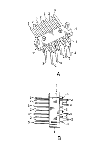
Figs. 1A and 1B show a contact assembly 1 incorporated in a
conventional differential signal connector which is different from the one
disclosed
in Patent Document 1 but is similar in configuration thereto. The contact
assembly 1 comprises a plurality of pairs of signal contacts 2, a plurality of
ground contacts 3, and an insulating housing 4 holding the signal contacts 2
and
the ground contacts 3. On the first connection side for connection to a
connection partner, the ground contacts 3 are arranged on both sides of each
pair
of signal contacts 2 so that a fixed-pitch contact array is formed. On the
other
hand, on the second connection side for connection to a board, the signal
contacts 2 and the ground contacts 3 are bent in a direction crossing the
contact
array so that the signal contacts 2 and the ground contacts 3 are arranged
zigzag
in two rows.
Fig. 2 shows a board 5 for mounting thereon the differential signal
connector including the contact assembly 1 of Figs. 1A and 1B. The board 5 is
formed with a plurality of through holes 6. The through holes 6 are arranged
zigzag in two rows so as to correspond to the arrangement of the signal
contacts
2 and the ground contacts 3 on the second connection side.
When the differential signal connector is mounted on the board 5, the
signal contacts 2 and the ground contacts 3 are respectively inserted into the
through holes 6. Lands 7 each in the form of a doughnut-shaped conductor
pattern are respectively formed around openings of the through holes 6.
Further, wiring patterns 8 are drawn out in parallel along the board 5 from
only
those lands 7 which are formed corresponding to the through holes 6 adapted to
be inserted with the signal contacts 2. Therefore, each signal contact 2 is
CA 02866439 2014-10-08
3
connected to the wiring pattern 8 through the through hole 6 and the land 7.
In the above-mentioned differential signal connector, arranging the signal
contacts and the ground contacts zigzag in two rows on the second connection
side, itself, easily makes it possible to reduce the size of the connector.
However, if the connector is actually reduced in size this way, there arise
the
following problems due to the occurrence of a difference in length between the
differential signal contacts forming a pair.
As shown in Fig. 3, a plurality of pairs of signal contacts and a plurality of
ground contacts can be collectively manufactured by punching a single
conductor
plate and then carrying out bending. In order to facilitate this manufacturing
process, it is common sense of those skilled in the art that forward ends of
the
contacts are arranged at regular intervals in a bent state and that the number
of
times of contact bending is set to two. However, in order to arrange the
forward
ends of the contacts at regular intervals in the bent state, there occurs a
difference in length between the differential signal contacts forming a pair
as is
well seen from a developed state of the contacts shown in Fig. 3. This
difference in length causes a propagation time difference (skew) between a
differential signal pair in a differential signal connector.
Further, due to this difference in length, there is a case where, on the
second connection side, i.e. on a board, the differential signal contacts
forming a
pair are separated in two rows, i.e. not arranged in the same row. This also
applies to the ground contacts arranged on both sides of such a pair of
differential
signal contacts. In this case, there occurs a difference in length between a
pair
of wiring patterns connected to such a pair of differential signal contacts,
as is
also seen from Fig. 2 where there are shown the wiring patterns with different
lengths which are drawn out from the lands formed in different rows. This
difference in length between the pair of wiring patterns also causes a skew
between a differential signal pair.
CA 02866439 2014-10-08
4
Summary of the Invention:
It is therefore an exemplary object of this invention to provide a
differential signal connector that is small in size and that can reduce a skew
between a differential signal pair.
Other objects of the present invention will become clear as the
description proceeds.
According to an exemplary aspect of the present invention, there is
provided a differential signal connector comprising a plurality of pairs of
signal
contacts, a plurality of ground contacts, and an insulating housing holding
the
signal contacts and the ground contacts, wherein the differential signal
connector
has a first connection side for connection to a connection partner and a
second
connection side for connection to a board, wherein, on the first connection
side,
the ground contacts are arranged on both sides of each pair of signal contacts
so
that a contact array of a fixed pitch is formed, and wherein, on the second
connection side, the ground contacts are arranged in a first row so as to be
spaced apart from each other, while the pairs of signal contacts, which are
adjacently arranged on both sides of the ground contact on the first
connection
side, are arranged so as to be allocated in a second row and a third row which
are located on both sides of the first row so that the pairs of signal
contacts are
arranged zigzag on the second connection side.
According to another exemplary aspect of the present invention, there is
provided a lead frame as an intermediate member for forming a contact group of
a connector, comprising a plurality of first leads arranged in a plane, second
leads
arranged so as to form a pair between the first leads, and a connecting
portion
connecting the first leads and the second leads on one end side, wherein a
pitch
of the pair of second leads is made greater on the other end side than on the
one
end side, and wherein the first leads each have a first straight portion
extending
from the connecting portion, a first offset portion extending obliquely from
the first
straight portion so as to be away from the second lead, and a second straight
CA 02866439 2014-10-08
portion extending from the first offset portion in the same direction as the
first
straight portion.
According to still another exemplary aspect of the present invention, there
is provided a differential signal connector comprising a contact group using
as an
intermediate member the above-mentioned lead frame, wherein the first leads
and the second leads are respectively bent in the direction crossing the plane
at
the first bending intended portions and the second bending intended portions
and
are respectively bent in the direction crossing the plane at the additional
bending
intended portions, and wherein the connecting portion is cut off from the
first
leads and the second leads.
According to yet another aspect of the present invention, there is
provided a differential signal connector comprising a plurality of ground
contacts
arranged at an interval from each other and a plurality of signal contacts
arranged
so as to form pairs each between the ground contacts, wherein one end of each
of the ground contacts and one end of each of the signal contacts are
adjacently
arranged in a plane on a first connection side of the connector, wherein the
ground contacts and the signal contacts extend in parallel to each other from
the
ends and then are bent at a right angle in the same direction at positions
offset
from each other, wherein, on a second connection side of the connector, the
other ends of the adjacent ground contacts are located at both ends of a long
side of a trapezoid while the other ends of the signal contacts forming each
pair
are located at both ends of a short side of the trapezoid, wherein, in order
to
increase a distance between the other ends of the signal contacts forming each
pair, both signal contacts are bent outward away from each other in the
vicinity of
the other ends thereof, and wherein the ground contacts each have an offset
portion between its portion bent at the right angle and the other end thereof.
Brief Description of the Drawings:
Figs. 1A and 1B show a contact assembly incorporated in a conventional
CA 02866439 2014-10-08
6
differential signal connector, wherein Fig. 1A is a perspective view and Fig.
1B is
a bottom view;
Fig. 2 is a bottom view of a board for mounting thereon the conventional
differential signal connector;
Fig. 3 is a contact development view (a lead frame with a carrier) in the
manufacture of signal contacts and ground contacts included in the contact
assembly of Figs. 1A and 1B;
Figs. 4A to 4D show a state where a differential signal connector
according to a first embodiment of this invention is mounted on a board,
wherein
Fig. 4A is a front view, Fig. 4B is a right side view, Fig. 4C is a bottom
view, and
Fig. 4D is a cross-sectional view taken along line Id-Id of Fig. 4A;
Figs. 5A to 5D show a lower contact assembly incorporated in the
differential signal connector of Figs. 4A to 4D, wherein Fig. 5A is a
perspective
view, Fig. 5B is a right side view, Fig. 5C is a rear view, and Fig. 5D is a
bottom
view;
Fig. 6 is a plan view of a member for use in the manufacture of signal
contacts and ground contacts included in the lower contact assembly of Figs.
5A
to 5D;
Fig. 7 is a plan view of a lead frame obtained by cutting off a carrier from
the member of Fig. 6;
Fig. 8 is an enlarged view of a main portion of Fig. 7;
Fig. 9 is an external perspective view of a first modification of the
differential signal connector of Figs. 4A to 4D;
Fig. 10 is a rear view of the differential signal connector of Fig. 9;
Fig. 11 is an exploded perspective view, seen from one direction, of the
differential signal connector of Fig. 9;
Fig. 12 is an exploded perspective view, seen from another direction, of
the differential signal connector of Fig. 9;
Figs. 13A and 13B are diagrams for explaining one process in the
CA 02866439 2014-10-08
7
manufacture of the differential signal connector of Fig. 9;
Fig. 14 is a perspective view showing an assembled state of internal
components of the differential signal connector of Fig. 9;
Fig. 15 is an exploded perspective view of a second modification of the
differential signal connector of Figs. 4A to 4D;
Fig. 16 is a perspective view showing an assembled state of internal
components of the differential signal connector of Fig. 15;
Fig. 17 is a perspective view of an upper contact assembly as one
component of the differential signal connector of Fig. 15;
Fig. 18 is a plan view showing one example of a contact group included in
the upper contact assembly of Fig. 17;
Fig. 19 is a plan view showing another example of a contact group
included in the upper contact assembly of Fig. 17;
Fig. 20 is a cross-sectional perspective view of a lower contact assembly
as one component of the differential signal connector of Fig. 15;
Fig. 21 is a perspective view of only a contact group included in the lower
contact assembly of Fig. 20;
Fig. 22 is a plan view of one example of a lead frame used in the
manufacture of the contact group of Fig. 21;
Fig. 23 shows three views of the contact group of Fig. 21;
Fig. 24 is a perspective view showing a state where a differential signal
connector according to a second embodiment of this invention is mounted on a
board;
Fig. 25 is an enlarged cross-sectional view of a main portion of Fig. 24;
Fig. 26 is a perspective view of a contact group included in the differential
signal connector of Figs. 24 and 25;
Fig. 27 is a plan view of a lead frame used in the manufacture of the
contact group of Fig. 26;
Fig. 28 is an enlarged view of a main portion of Fig. 27;
CA 02866439 2014-10-08
8
Fig. 29 is a plan view of a modification of the lead frame used in the
manufacture of the contact group of Fig. 26; and
Fig. 30 is an enlarged view of a main portion of Fig. 29.
Exemplary Embodiments:
Referring to Figs. 4A to 8, a differential signal connector 10 according to a
first embodiment of this invention will be described.
Figs. 4A to 4D show a state where the differential signal connector 10 is
mounted on a printed board 11. The differential signal connector 10 is a
printed
board mount-type 20-pin connector having contacts in upper and lower two rows
and is mounted on the printed board 11 when it is used. The front side, for
connection to a mating connector (not illustrated) serving as a connection
partner,
of the differential signal connector 10 is called a first connection side,
while its
bottom side for connection to the printed board 11 is called a second
connection
side. On the first connection side, a fitting projection 12 is provided for
fitting to
the mating connector. The fitting projection 12 has a shape extending
laterally in
parallel to the connector fitting plane. The second connection side will be
described in detail later.
The printed board 11 used herein is a multilayer board. The printed
board 11 is formed with a number of through holes 13 as seen from Fig. 4C
showing a lower surface 11a of the printed board 11. Lands 14 each in the form
of a doughnut-shaped conductor pattern are respectively formed around
openings of the through holes 13. Further, wiring patterns 15 are drawn out in
parallel along the board 11 from some of the lands 14. The positions and roles
of the through holes 13 will be clarified later.
The differential signal connector 10 comprises an upper contact assembly
16, a lower contact assembly 17, and a conductive connector shell 18
surrounding the upper and lower contact assemblies 16 and 17 as a whole. The
upper contact assembly 16 comprises a number of conductive upper contacts 19,
CA 02866439 2014-10-08
9
called additional contacts herein, and an insulating upper housing 21 holding
the
upper contacts 19. The upper contacts 19 have forward ends arranged in the
upper part of the fitting projection 12, then extend rearward, and then are
bent
downward at a right angle so that lower ends of the upper contacts 19 are
soldered to wiring patterns on an upper surface (not illustrated) of the
printed
board 11 in an SMT structure. The connector shell 18 has two pairs of fixing
legs 18a and 18b adapted to be fixed to the printed board 11. By engagement of
the fixing legs 18a and 18b with the printed board 11, the differential signal
connector 10 is firmly fixed to the printed board 11. The lower contact
assembly
17 will be described in detail later.
Next, referring to Figs. 5A to 5D in addition to Figs. 4A to 4D, the lower
contact assembly 17 will be described in detail.
The lower contact assembly 17 comprises three pairs of conductive
signal contacts 22, four conductive ground contacts 23, and an insulating
lower
housing 24 holding the signal contacts 22 and the ground contacts 23. On the
first connection side of the lower housing 24, there is formed a contact array
of a
fixed pitch (preferably 0.7mm or less in a miniaturized display port
connector)
which extends in a first direction A1 in a state where the ground contacts 23
are
arranged on both sides of each pair of signal contacts 22.
All of the signal contacts 22 and the ground contacts 23 extend rearward
in a second direction A2 perpendicular to the first direction A1 to pass
through the
lower housing 24 and then are bent at a right angle on the opposite side of
the
lower housing 24 to extend downward in a third direction A3 perpendicular to
the
first and second directions A1 and A2. In the following description, the
signal
contacts 22 and the ground contacts 23 may also be collectively called lower
contacts 25.
As seen from Figs. 4A to 4D, on the first connection side of the differential
signal connector 10, the lower contacts 25 are arranged in the lower part of
the
fitting projection 12 so as to face the upper contacts 19 at a distance
therefrom.
CA 02866439 2014-10-08
As a consequence, the mating connector is brought into contact with the upper
contacts 19 and the lower contacts 25 when it is fitted to the fitting
projection 12,
so that the mating connector is electrically connected to the differential
signal
connector 10. Herein, a portion, which is brought into contact with the mating
connector, of each lower contact 25 is called a connector contact portion.
On the other hand, on the second connection side of the differential
signal connector 10, the lower contacts 25 are respectively inserted into the
through holes 13 of the printed board 11 and are respectively connected to the
lands 14 by soldering on the lower surface 11a of the printed board 11. Since
the lower contacts 25 are soldered on the lower surface lla of the printed
board
11, the soldering condition can be easily checked visually when the
differential
signal connector 10 is mounted on the printed board 11. Herein, a portion,
which is inserted into the through hole 13, of each lower contact 25 is called
a
board connecting portion.
When the cross-sectional shape of the lower contact 25 is square, the
diameter of the through hole 13 of the printed board 11 is designed to be at
least
slightly greater than a diagonal length of the lower contact 25. Further, the
lands
14 are formed around the through holes 13 and it is necessary to ensure
insulation between the adjacent through holes 13. Taking these into account,
it
is preferable to set an interval of about 0.8mm for the through holes 13.
In Figs. 5A to 5D, the board connecting portions of the lower contacts 25
are arranged in three parallel rows which extend in the second direction A2
and
which are spaced apart from each other in the first direction A1.
Specifically, the
board connecting portions of the ground contacts 23 are arranged in a first
row
R1 so as to be spaced apart from each other, while the pairs of signal
contacts 22
whose connector contact portions are arranged between the ground contacts 23
are arranged so as to be allocated in a second row R2 and a third row R3 which
are located on both sides of the first row R1. As a result, as is well seen
from
Figs. 5A to 5D, the board connecting portions of the pairs of signal contacts
22
CA 02866439 2014-10-08
11
are arranged zigzag on both sides of the first row R1.
Herein, the signal contacts 22 arranged in the second row R2 are
designed to have substantially the same length, while the signal contacts 22
arranged in the third row R3 are designed to have substantially the same
length.
That is, the lengths of the pair of signal contacts 22 arranged in the same
row are
set to be equal to each other. Then, the pairs of signal contacts 22 are
allocated
to the second row R2 and the third row R3 by the difference in bending thereof
from each other, specifically, the difference in bending position thereof from
each
other, between the first connection side and the second connection side. The
ground contacts 23 are arranged in the first row R1 by the difference in
bending
position thereof from the signal contacts 22 between the first connection side
and
the second connection side. Instead of providing the difference in bending
position, the signal contacts 22 and the ground contacts 23 can be arranged in
three rows on the second connection side by the difference in number of times
of
bending or both may be jointly used.
Further, on the second connection side, each pair of signal contacts 22
are arranged at a position corresponding to between the adjacent ground
contacts 23 and, further, the pitch of each pair of signal contacts 22 is
designed to
be slightly greater than the pitch of the contact array.
On the second connection side, the ground contacts 23 are each
arranged at a position corresponding to between the pairs of signal contacts
22
and, further, the ground contacts 23 and the pairs of signal contacts 22,
which are
adjacently arranged on both sides of each ground contact 23 on the first
connection side, are arranged in directions obliquely crossing the first,
second,
and third rows R1, R2, and R3.
On the other hand, naturally, the through holes 13 of the printed board 11
are formed at positions corresponding to the above-mentioned arrangement of
the signal contacts 22 and the ground contacts 23 on the second connection
side.
Herein, each pair of the adjacent signal contacts 22 are for connecting
CA 02866439 2014-10-08
12
lines adapted to transmit a differential signal pair comprising signals having
opposite phases and thus will be respectively called a +Sig contact and a -Sig
contact in the following description. Further, among the through holes 13, the
through hole 13 adapted to be inserted with the +Sig contact will be called a
+Sig
through hole, the through hole 13 adapted to be inserted with the -Sig contact
will
be called a -Sig through hole, and the through hole 13 adapted to be inserted
with
the ground contact 23 will be called a GND through hole. Further, among the
wiring patterns 15, the wiring pattern 15 connected to the +Sig through hole
will
be called a +Sig wiring pattern and the wiring pattern 15 connected to the -
Sig
through hole will be called a -Sig wiring pattern.
According to the differential signal connector described above, since the
+Sig through hole and the -Sig through hole are arranged in parallel to the
connector fitting plane, the +Sig wiring pattern and the -Sig wiring pattern
can be
formed as wiring patterns extending rearward of the connector and being equal
in
length and parallel to each other on the lower surface 11a of the printed
board 11
as the multilayer board. As a consequence, the skew between the differential
signal pair is small. Although the description has been given of the case
where
the lines adapted to transmit the pair of differential signals are connected,
this
also applies to the case where a plurality of pairs of differential signals
are
transmitted. The same effect can be obtained.
The contact group as a gathering of the three pairs of conductive signal
contacts 22 and the four conductive ground contacts 23 can be easily formed
from a single conductor plate by pressing. In this case, the shape shown in
Fig.
6 is first obtained. Then, a carrier 26 is cut off, thereby forming a lead
frame 30
shown in Figs. 7 and 8 as one example of an intermediate member.
In Figs. 7 and 8, the lead frame 30 comprises a plurality of first leads 31
arranged in a plane, second leads 32 arranged so as to form pairs each between
the first leads 31, third leads 33 arranged so as to form a pair between the
first
leads 31, and a connecting portion 34 connecting the first leads 31, the
second
CA 02866439 2014-10-08
13
leads 32, and the third leads 33 on one end side. The length of the second
lead
32 from the connecting portion 34 is made shorter than that of the first lead
31.
The length of the third lead 33 from the connecting portion 34 is made longer
than
that of the first lead 31. Further, when punching a metal plate, a pitch P2 of
each of the pairs of second leads 32 and the pair of third leads 33 on the
other
end side, i.e. on the free end side, is made greater than a pitch P1 thereof
on the
one end side, so that each pair of leads 32, 33 approach the first leads 31 on
the
free end side.
The first leads 31 each have a first straight portion 35 extending from the
connecting portion 34, a first offset portion 36 extending obliquely from the
first
straight portion 35 so as to be away from a portion, with the greater pitch
P2, of
the second lead 32, a second straight portion 37 extending from the first
offset
portion 36 in the same direction as the first straight portion 35, a second
offset
portion 38 extending obliquely from the second straight portion 37 so as to
approach the second lead 32, and a third straight portion 39 extending from
the
second offset portion 38 on an extension line of the first straight portion
35.
Further, the first leads 31 each have, in the first straight portion 35, a
first
bending intended portion 41 for bending in a direction crossing the above-
mentioned plane. The second leads 32 each have, at a position between its
portion with the greater pitch P2 and the connecting portion 34 and adjacent
to
the portion with the greater pitch P2, a second bending intended portion 42
for
bending in the direction crossing the above-mentioned plane.
In the lead frame 30 of Figs. 7 and 8, although the portions with the
greater pitch P2 are provided on the free end side of the second leads 32
forming
each pair, the distance between each first lead 31 and the corresponding
second
lead 32 can be made relatively large due to the presence of the first offset
portion
36. As a consequence, the lead frame 30 can be easily manufactured by press-
punching.
Further, the lead frame 30 is bent at the first bending intended portions 41
CA 02866439 2014-10-08
14
and the second bending intended portions 42 and then the connecting portion 34
is cut off. In this way, it is possible to easily obtain the contact group
comprising
the six signal contacts 22 and the four ground contacts 23 of the lower
contact
assembly shown in Figs. 5A to 5D.
Since the greater pitch P2 is provided on the free end side of each of the
pairs of second leads 32 and the pair of third leads 33 in the lead frame 30,
the
distance between the signal contacts 22 in the second and third rows R2 and R3
in Figs. 5A to 5D is made large so that it is possible to easily provide the
through
holes and the lands in the printed board 11 with sufficient electrical
insulation
therebetween. In addition, since the ground contacts 23 and the first and
second signal contacts 22 are arranged in the three different rows, it is
possible
to set the distance therebetween to be large and thus to sufficiently ensure
electrical insulation between differential signal pairs. As a consequence, it
is
possible to easily achieve pitch-narrowing of the contact group.
Further, since each first lead 31 is provided with the first offset portion 36
that extends obliquely so as to be away from the portion, with the greater
pitch
P2, of the corresponding second lead 32, it is possible to make large the
distance
between the second straight portion 37 following the first offset portion 36
and the
portion, with the greater pitch P2, of the second lead 32. As a consequence,
punching is easily applied and thus it is possible to provide the lead frame
30 that
contributes to the manufacture of a narrow-pitch contact group.
Referring to Figs. 9 to 12, a first modification of the differential signal
connector described above will be described. The same reference symbols are
assigned to the same or similar portions, thereby omitting explanation
thereof.
This first modification comprises an upper contact assembly 16, a lower
contact assembly 17, and an insulating locator 43 incorporated in a connector
shell 18.
A number of upper contacts 19 each have a horizontal portion 19a
arranged on an upper surface of a fitting projection 12, a bent portion 19b
CA 02866439 2014-10-08
exposed rearward of an upper housing 21 from a rear end of the horizontal
portion 19a and bent downward, a vertical portion 19c extending vertically
downward from the bent portion 19b, and a connecting portion 19d bent at a
right
angle from a lower end of the vertical portion 19c and adapted to be soldered
to a
wiring pattern on an upper surface of a mounting object such as a printed
board
in an SMT structure. Hereinbelow, the upper contacts 19 may also be
collectively called a contact group.
The upper contacts 19 are held by the upper housing 21 at portions of the
horizontal portions 19a by insert molding. The portion, held by the upper
housing 21, of each horizontal portion 19a is called a holding portion herein.
A substantially rectangular parallelepiped dielectric 44 is attached to the
vertical portions 19c of the upper contacts 19 by insert molding. The
dielectric
44 covers most of each vertical portion 19c in a contact manner from the
outside
so as to be integral with the upper contacts 19. As a result, the arrayed
state of
the contact group is held by the dielectric 44. Further, engaging projections
44a
are respectively formed at both ends, in an array direction of the contact
group, of
the dielectric 44. The portion, covered with the dielectric 44, of each
vertical
portion 19c is called an intermediate portion herein.
Like the lower contact assembly of the differential signal connector which
has been described with reference to Figs. 4A to 8, the lower contact assembly
17 comprises an insulating lower housing 24 and a number of conductive lower
contacts 25 including signal contacts 22 and ground contacts 23 which are held
in
array by the lower housing 24. The lower housing 24 has a pair of posts 24a
for
positioning with the upper housing 21. The lower contacts 25 each have a
horizontal portion 25a arranged along a lower surface of the fitting
projection 12
of the upper housing 21 and a vertical portion 25b exposed rearward of the
lower
housing 24 and extending vertically downward. A lower end portion of the
vertical portion 25b of the lower contact 25 serves as a terminal portion 25c
adapted to be inserted into each of through holes formed in the mounting
object
CA 02866439 2014-10-08
16
and fixed by soldering.
The locator 43 has on its lower surface a pair of positioning bosses 45 for
fitting into positioning holes (not illustrated) of the mounting object. The
locator
43 has on its rear surface a recess 46 which coincides with the shape and size
of
the dielectric 44. On mutually opposite side surfaces of the recess 46,
engaging
projections 46a corresponding to the engaging projections 44a of the
dielectric 44
are formed. Further, a key groove 46b is formed on a bottom surface of the
recess 46.
The connector shell 18 has a plurality of fixing legs 18a and 18b. By
engagement of the fixing legs 18a and 18b with the mounting object, a
differential
signal connector 10 is firmly fixed to the mounting object.
Herein, referring also to Figs. 13A and 13B, a method of manufacturing
the upper contact assembly 16 will be described. Before forming the bent
portions 19b in the upper contacts 19, the upper housing 21 and the dielectric
44
are simultaneously insert-molded with respect to the contact group, thereby
obtaining a configuration shown in Fig. 13A. Then, the contact group is
subjected to bending, thereby forming the bent portions 19b as shown in Fig.
13B. In this event, since both sides of the bent portions 19b are integrally
held
by the upper housing 21 and the dielectric 44, the contact group can be easily
bent into a predetermined shape without misaligning the contact group. Symbol
44b denotes a key corresponding to the key groove 46b.
As described above, it is advantageous in terms of the manufacturing
process to simultaneously insert-mold the upper housing 21 and the dielectric
44
with respect to the contact group. However, alternatively, the upper housing
21
and the dielectric 44 may be formed separately.
Fig. 14 shows a state where the upper contact assembly 16 and the lower
contact assembly 17 are mounted to the locator 43. When mounting the upper
contact assembly 16 to the locator 43, the dielectric 44 is inserted into the
recess
46 of the locator 43 while fitting the key 44b shown in Figs. 13A and 13B into
the
CA 02866439 2014-10-08
17
key groove 46b shown in Fig. 11. After the insertion, the dielectric 44 is
fixedly
fitted in the recess 46 by engagement of the engaging projections 44a with the
engaging projections 46a.
Further, the upper contact assembly 16, the lower contact assembly 17,
and the locator 43 are collectively surrounded by the connector shell 18, so
that
the connector 10 shown in Figs. 9 and 10 is obtained. It is to be noted that
the
locator 43 is partially projected and exposed to the outside of the connector
shell
18 on both sides of the connector 10.
According to the differential signal connector described with reference to
Figs. 9 to 14, since it is configured such that the portions, exposed from the
upper
housing 21, of the upper contacts 19 are covered by the insert molding of the
dielectric 44 in the contact manner and that the dielectric 44 is fitted and
coupled
to the locator 43 adapted to be positioned with respect to the mounting
object, it
is possible to achieve impedance matching and to prevent positional deviation
of
the connecting portions 19d of the upper contacts 19. Further, since the
locator
43 is partially projected to the outside of the connector shell 18, the
surface
mounting of the connector with high positional accuracy is enabled by image
recognition of the projected portions.
Referring to Figs. 15 and 16, a second modification of the differential
signal connector described above will be described. The same reference
symbols are assigned to the same or similar portions, thereby omitting
explanation thereof.
In Fig. 15, before mounting an upper contact assembly 16, vertical
portions 19c of upper contacts 19 are entirely exposed to the outside. On the
other hand, a rear surface of a locator 43 is formed with a plurality of
parallel
grooves 47 which are arranged at the same pitch as the vertical portions 19c
and
extend vertically. These grooves 47 each have a size that can receive
substantially the entirety of the vertical portion 19c of the upper contact 19
with a
little gap. Therefore, the operation of inserting the vertical portions 19c
into the
CA 02866439 2014-10-08
18
grooves 47 is easy.
Fig. 16 shows a state where the upper contact assembly 16 and a lower
contact assembly 17 are mounted to the locator 43. When mounting the upper
contact assembly 16 to the locator 43, the vertical portions 19c of the upper
contacts 19 are respectively inserted into the grooves 47 of the locator 43.
As a
result, an effect is achieved similar to that of the dielectric 44 of the
differential
signal connector 10 described with reference to Figs. 9 to 14. Thereafter, a
resin
having a permittivity equal to or different from that of the locator 43 is
filled in the
grooves 47 so as to cover substantially the entirety of the vertical portions
19c of
the upper contacts 19 and then is cured so that the degree of freedom of
impedance adjustment becomes high. The portion, covered with the cured
resin, of each vertical portion 19c is called an intermediate portion herein.
Also in this modification, there is obtained a connector having the same
external appearance as the differential signal connector 10 of Fig. 9.
According to the connector described with reference to Figs. 15 and 16,
since it is configured such that the dielectric in the form of the cured resin
covers
the portions, exposed from an upper housing 21, of the upper contacts 19 in a
contact manner and is coupled to the locator 43 adapted to be positioned with
respect to a mounting object, it is possible to achieve impedance matching and
to
prevent positional deviation of connecting portions 19d of the upper contacts
19.
Further, since the locator 43 is partially projected to the outside of a
connector
shell 18, the surface mounting of the connector with high positional accuracy
is
enabled by image recognition of the projected portions.
Fig. 17 is a perspective view, seen from a different direction, of the upper
contact assembly 16 as one component of the differential signal connector of
Fig.
15. The same reference symbols are assigned to the same or similar portions,
thereby omitting explanation thereof.
Referring to Fig. 18, a first example of a contact group included in the
upper contact assembly 16 will be described.
CA 02866439 2014-10-08
19
The contact group of Fig. 18 comprises four ground contacts 19-1
arranged so as to be spaced apart from each other and six signal contacts 19-2
arranged so as to form three pairs each between the ground contacts 19-1. The
ground contacts 19-1 are each used for connection to a ground line while the
signal contacts 19-2 are each used for connection to a signal line. The four
contacts arranged in the order of the ground contact 19-1, the signal contact
19-
2, the signal contact 19-2, and the ground contact 19-1 form one contact set
51
and, by repeating the contact sets 51 while partially overlapping each other,
the
contact group is formed. Since all the contact sets 51 have the same
structure,
only one of them will be described herein.
In all of the intermediate two signal contacts 19-2 and the two ground
contacts 19-2 on both sides thereof, bent portions 19b are provided at the
same
position in the longitudinal direction of the contacts. That is, the bent
portions
19b are provided in one row in an array direction of the contacts.
Accordingly,
on one end side in the longitudinal direction of the contacts (lower side in
Fig. 18),
the four contacts of the contact set 51 are arranged in one row along an upper
surface of a fitting projection 12 as shown in Fig. 17, while, on the other
end side
(upper side in Fig. 18), the four contacts of the contact set 51 are inserted
into the
grooves 47 of the locator 43 shown in Fig. 15 so as to be arranged in one row
along the rear surface of the locator 43.
Further, the four contacts of the contact set 51 respectively have holding
portions 52 adapted to be held by the upper housing 21 of Fig. 17 by insert
molding. That is, by the engagement of the holding portions 52 with the upper
housing 21, the contact group is firmly held by the upper housing 21.
The holding portion 52 of each contact is provided with a plurality of (two
in this example) projecting portions 53 as one kind of a differently shaped
portion
that changes the contact width. In each contact, the projecting portions 53
are
integrally formed at corresponding positions of both side surfaces of the
contact
so as to be symmetric with respect to the center of the contact. The forming
CA 02866439 2014-10-08
positions of the projecting portions 53 in the longitudinal direction of the
contacts
differ from each other between the ground contact 19-1 and the signal contact
19-
2. In the
illustrated example, the projecting portions 53 of the ground contact 19-
1 are formed on the side close to the bent portion 19b in the holding portion
52
while the projecting portions 53 of the signal contact 19-2 are formed on the
side
far from the bent portion 19b in the holding portion 52. This, however, may be
reversed. At any rate, the projecting portions 53 are formed to be symmetric
with respect to the center of the array of the intermediate two signal
contacts 19-
2, i.e. with respect to the center of the array of the four contacts.
Since the projecting portions 53 are formed to be symmetric as described
above, the symmetry of differential signal transmission lines comprising the
four
contacts is maintained and, therefore, the high-frequency characteristics of
the
connector are not degraded by providing the projecting portions 53. Further,
since the projecting portions 53 are formed at the plurality of different
positions in
the longitudinal direction of the contacts, the distance between the adjacent
contacts can be made relatively large and thus pressing is easily applied.
Referring to Fig. 19, a second example of a contact group included in the
upper contact assembly 16 will be described. The same reference symbols are
assigned to the same or similar portions as those in Fig. 18, thereby omitting
explanation thereof.
Also in the contact group of Fig. 19, in all of intermediate two signal
contacts 19-2 and two ground contacts 19-2 on both sides thereof, bent
portions
19b are provided at the same position in the longitudinal direction of the
contacts.
That is, the bent portions 19b are provided in one row in an array direction
of the
contacts. Accordingly, on one end side in the longitudinal direction of the
contacts (lower side in Fig. 19), the four contacts of a contact set 51 are
arranged
in one row along an upper surface of a fitting projection 12 as shown in Fig.
17,
while, on the other end side (upper side in Fig. 19), the four contacts of the
contact set 51 are inserted into the grooves 47 of the locator 43 shown in
Fig. 15
CA 02866439 2014-10-08
21
so as to be arranged in one row along the rear surface of the locator 43.
A holding portion 52 of each contact is provided with a plurality of (two in
this example) cutouts 54 as one kind of a differently shaped portion that
changes
the contact width. In each contact, although the cutouts 54 are provided on
both
side surfaces, the cutouts 54 are formed at different positions in the
longitudinal
direction of the contact so as to be asymmetric with respect to the center of
the
contact. The forming positions of the cutouts 54 in the longitudinal direction
of
the contacts differ from each other between the adjacent contacts. At any
rate,
the cutouts 54 are formed to be symmetric with respect to the center of the
array
of the intermediate two signal contacts 19-2, i.e. with respect to the center
of the
array of the four contacts.
Since the cutouts 54 are formed to be symmetric as described above, the
symmetry of differential signal transmission lines comprising the four
contacts is
maintained and, therefore, the high-frequency characteristics of the connector
are
not degraded by providing the cutouts 54. Further, since the cutouts 54 are
formed at the plurality of different positions in the longitudinal direction
of the
contacts, the distance between the adjacent contacts can be made relatively
large and thus pressing is easily applied.
Referring to Figs. 20 and 21, one example of a contact group included in
the lower contact assembly 17 will be described.
In the contact group shown in Figs. 20 and 21, three pairs of signal
contacts 22 are respectively arranged between four ground contacts 23 which
are
arranged so as to be spaced apart from each other. The ground contacts 23 are
each used for connection to a ground line while the signal contacts 22 are
each
used for connection to a signal line. The four contacts arranged in the order
of
the ground contact 23, the signal contact 22, the signal contact 22, and the
ground contact 23 form one contact set 61 and, by repeating the contact sets
61
while partially overlapping each other, the contact group is formed. Since all
the
contact sets 61 have the same structure, only one of them will be described
CA 02866439 2014-10-08
22
herein.
In the intermediate two signal contacts 22 and the two ground contacts 23
on both sides thereof, bent portions 22b and 23b are provided at different
positions in the longitudinal direction of the contacts. Accordingly, on one
end
side in the longitudinal direction of the contacts (upper left side in Fig.
20), the
four contacts of the contact set 61 are arranged in one row along one plane,
while, on the other end side (lower right side in Fig. 20), the pair of signal
contacts 22 and the two ground contacts 23 on both sides thereof are arranged
in
different rows, i.e. in the rows R1-R3 in Figs. 5A to 5D. Further, the pitch
of the
intermediate two signal contacts 22 is made greater on the other end side than
on
the one end side.
Further, the four contacts of the contact set 61 respectively have holding
portions 62 adapted to be held by a lower housing 24 by insert molding. That
is,
by the engagement of the holding portions 62 with the lower housing 24, the
contact group is firmly held by the lower housing 24.
The holding portion 62 of each contact is provided with a plurality of (two
in this example) projecting portions 63 as one kind of a differently shaped
portion
that changes the contact width. The function of these projecting portions 63
is
the same as that of the projecting portions 53 in the contact group shown in
Fig.
18.
Since the projecting portions 63 of the contact group included in the lower
contact assembly 17 are also formed to be symmetric, the symmetry of
differential signal transmission lines comprising the four contacts is
maintained
and, therefore, the high-frequency characteristics of the connector are not
degraded by providing the projecting portions 63. Further, since the
projecting
portions 63 are formed at a plurality of different positions in the
longitudinal
direction of the contacts, the distance between the adjacent contacts can be
made relatively large and thus pressing is easily applied.
Also in the contact group included in the lower contact assembly 17,
CA 02866439 2014-10-08
23
cutouts which are the same as the cutouts 54 in the contact group shown in
Fig.
19 can be provided instead of the projecting portions 63. It is needless to
say
that the same function and effect can be obtained also in that case.
Fig. 22 is a plan view showing a state where a single metal plate is
pressed into a lead frame and Fig. 23 shows three views of the contact group
of
Fig. 21 obtained from the lead frame of Fig. 22. In the contact set 61, the
two
ground contacts 23 on both sides of the intermediate two signal contacts 22
are
respectively provided with escape portions 64 being away from the intermediate
two signal contacts 22, at the position where the pitch of the intermediate
two
signal contacts 22 is increased. As a result, since the distance between the
signal contact 22 and the ground contact 23 is made large at the position
where
the escape portion 64 is provided, the formation by pressing is facilitated.
Next, referring to Figs. 24 and 25, a connector 70 according to a second
embodiment of this invention will be described.
This connector 70 is a differential signal connector adapted to be
mounted on a printed board 71 at its end portion. The connector 70 comprises a
number of conductive upper contacts (contact group) 72, a number of conductive
lower contacts 73, an insulating housing 74 holding the contacts 72 and 73,
and a
conductive connector shell 75 surrounding them. The printed board 71 is
formed with a cutout 71a at its end portion. The contacts 72 and 73 are
respectively arranged in a direction perpendicular to the sheet surface in
Fig. 25.
The housing 74 has a first portion 74a adapted to be inserted into the
cutout 71a of the printed board 71 and a second portion 74b extending from the
first portion 74a along a lower surface of the printed board 71. Each upper
contact 72 extends in the first portion 74a and then in the second portion 74b
with
bending and has a terminal portion 72a which passes through a through hole
formed in the printed board 71 so as to be connected by soldering. Each lower
contact 73 extends in the first portion 74a and then in the second portion 74b
with
bending and has a terminal portion 73a which is connected by soldering to the
CA 02866439 2014-10-08
24
lower surface of the printed board 71. A mating connector (not illustrated)
serving as a connection partner is fitted to the first portion 74a so as to be
electrically connected to the upper contacts 72 and the lower contacts 73.
Referring to Fig. 26, only the upper contacts 72 are collectively shown as
a contact group. As seen from Fig. 26, the upper contacts 72 are divided into
three kinds based on the positions of the terminal portions 72a. That is, the
terminal portions 72a are arranged in three rows. The upper terminal 72 whose
terminal portion 72a is arranged in an intermediate row R1 is called a ground
contact. The upper terminal 72 whose terminal portion 72a is arranged in a row
R2 on one side of the intermediate row R1 is called a first signal contact.
The
upper terminal 72 whose terminal portion 72a is arranged in a row R3 on the
other side of the intermediate row R1 is called a second signal contact.
Accordingly, the contact group of Fig. 26 comprises four ground contacts, four
first signal contacts, and two second signal contacts. The ground contacts are
each connected to a ground line of the printed board 71 while the first and
second
signal contacts are each connected to a signal line of the printed board 71.
As shown in Fig. 26, on the first connection side of the connector, one
end of each of the ground contacts and one end of each of the signal contacts
are adjacently arranged in a plane. Then, the ground contacts and the signal
contacts extend in parallel to each other and then are bent at a right angle
in the
same direction at positions offset from each other. As a consequence, on the
second connection side of the connector, the other ends (terminal portions
72a)
of the adjacent ground contacts are located at both ends of the long side of a
trapezoid while the other ends (terminal portions 72a) of the signal contacts
forming each pair are located at both ends of the short side of the trapezoid.
Further, in order to increase the distance between the other ends (terminal
portions 72a) of the signal contacts forming each pair, both signal contacts
are
slightly bent outward away from each other in the vicinity of the other ends
(terminal portions 72a) thereof as will be clarified later.
CA 02866439 2014-10-08
Referring to Figs. 27 and 28, a lead frame 80 is shown as one example of
an intermediate member for use in the manufacture of the above-mentioned
contact group.
The lead frame 80 is manufactured by punching a metal plate and
comprises a plurality of first leads 81 arranged in a plane, second leads 82
arranged so as to form pairs each between the first leads 81, third leads 83
arranged so as to form a pair between the first leads 81, and a connecting
portion
84 connecting the first leads 81, the second leads 82, and the third leads 83
on
one end side. The length of the second lead 82 from the connecting portion 84
is made shorter than that of the first lead 81. The length of the third lead
83 from
the connecting portion 84 is made longer than that of the first lead 81.
Further,
when punching the metal plate, a pitch P4 of each of the pairs of second leads
82
and the pair of third leads 83 on the other end side, i.e. on the free end
side, is
made greater than a pitch P3 thereof on the one end side, so that each pair of
leads 82, 83 approach the first leads 81 on the free end side.
The first leads 81 each have a first straight portion 85 extending from the
connecting portion 84, a first offset portion 86 extending obliquely from the
first
straight portion 85 so as to be away from a portion, with the greater pitch
P4, of
the second lead 82, a second straight portion 87 extending from the first
offset
portion 86 in the same direction as the first straight portion 85, a second
offset
portion 88 extending obliquely from the second straight portion 87 so as to
approach the second lead 82, and a third straight portion 89 extending from
the
second offset portion 88 on an extension line of the first straight portion
85.
Further, the first leads 81 each have, in the second straight portion 87, a
first bending intended portion 91 for bending in a direction crossing the
above-
mentioned plane. The second leads 82 each have, at a position between its
portion with the greater pitch P4 and the connecting portion 84 and adjacent
to
the portion with the greater pitch P4, a second bending intended portion 92
for
bending in the direction crossing the above-mentioned plane.
CA 02866439 2014-10-08
26
Further, the first leads 81 and the second leads 82 each have a plurality
of additional bending intended portions 93 between the connecting portion 84
and
the first offset portion 86 or between the connecting portion 84 and the
second
bending intended portion 92.
In the lead frame 80 of Fig. 27, although the portions with the greater
pitch P4 are provided on the free end side of the second leads 82 forming each
pair, the distance between each first lead 81 and the corresponding second
lead
82 can be made relatively large due to the presence of the first offset
portion 86.
As a consequence, the lead frame 80 of Fig. 27 can be easily manufactured by
press-punching.
Then, the lead frame 80 of Fig. 27 is bent at the first bending intended
portions 91, the second bending intended portions 92, and the additional
bending
intended portions 93 and then the connecting portion 84 is cut off. In this
way, it
is possible to easily obtain the contact group of Fig. 26 comprising the four
ground contacts, the four first signal contacts, and the two second signal
contacts.
Since the greater pitch P4 is provided on the free end side of each of the
pairs of second leads 82 and the pair of third leads 83 in the lead frame 80
of Fig.
27, the distance between the terminal portions 72a is made large in the rows
R2
and R3 of the contact group of Fig. 26 so that electrical insulation can be
sufficiently ensured between the adjacent first signal contacts and between
the
second signal contacts. In addition, since the terminal portions 72a of the
ground contacts and the first and second signal contacts are arranged in the
three different rows, it is possible to set the distance therebetween to be
large
and thus to sufficiently ensure electrical insulation therebetween. As a
consequence, it is possible to easily achieve pitch-narrowing of the contact
group.
Further, since each first lead 81 is provided with the first offset portion 86
that extends obliquely so as to be away from the portion, with the greater
pitch
P4, of the corresponding second lead 82, it is possible to make large the
distance
CA 02866439 2014-10-08
27
between the second straight portion 87 following the first offset portion 86
and the
portion, with the greater pitch P4, of the second lead 82. As a consequence,
punching is easily applied and thus it is possible to provide the lead frame
80 that
contributes to the manufacture of a narrow-pitch contact group.
Further, since the first bending intended portion 91 is provided in the
second straight portion 87 (between the first offset portion 86 and the second
offset portion 88), the distance from the first bending intended portion 91 to
the
free end, i.e. the length of the terminal portion 72a in Fig. 26, is shortened
as a
result. Accordingly, it is possible to easily achieve a reduction in the
height of
the connector.
Referring to Figs. 29 and 30, a lead frame 80' is shown as another
example of an intermediate member for use in the manufacture of the above-
mentioned contact group. The same reference symbols are assigned to the
same or similar portions as those in Figs. 27 and 28, thereby omitting
explanation
thereof.
In this lead frame 80', a first bending intended portion 91 is provided in a
first straight portion 85. Specifically, the first bending intended portion 91
is
provided at a position between a first offset portion 86 and a connecting
portion
84 and adjacent to the first offset portion 86. As a result of changing the
position
of the first bending intended portion 91, the positions of a second bending
intended portion 92 and additional bending intended portions 93 are located
slightly closer to the connecting portion 84, but the essential function is
the same
as that of the lead frame 80 shown in Fig. 27.
In this lead frame 80', the distance from the first bending intended portion
91 to the free end, i.e. the length of the terminal portion 72a in Fig. 26, is
slightly
longer as compared with the lead frame 80 of Fig. 27, while, the others are
the
same in function and effect as those of the lead frame 80 of Fig. 27.
In the case of a connector of the type adapted to be disposed in
substantially the same plane as a printed board as shown in Figs. 24 and 25,
CA 02866439 2014-10-08
28
each lead is provided with two additional bending intended portions 93 in
either of
the lead frames 80 and 80'. On the other hand, the lead frames 80 and 80' can
each also be used for a connector of the type adapted to be mounted on an
upper surface of a printed board as shown in Figs. 4A to 4D while, in this
case,
the additional bending intended portion 93 is not required.
While the invention has been particularly shown and described with
reference to exemplary embodiments thereof, the invention is not limited to
these
embodiments. It will be understood by those of ordinary skill in the art that
various changes in form and details may be made therein without departing from
the spirit and scope of the present invention as defined by the claims.