Note: Descriptions are shown in the official language in which they were submitted.
CA 02866862 2014-09-09
WO 2013/134628
PCT/US2013/029845
M2LC SYSTEM AND METHOD FOR CONTROLLING SAME
Inventors: Marc Aiello, Kenneth Berton and Walter Barie
CROSS-REFERENCE TO RELATED APPLICATION
[0001] This application claims the benefit under 35 U.S.C. 119(e) of the
earlier filing date of U.S. Provisional Patent Application No. 61/608,759
filed on
March 9, 2012.
BACKGROUND
[0002] This application discloses an invention which is related, generally and
in various embodiments, to a Modular Multilevel Converter (M2LC) system and a
method for controlling the M2LC system.
[0003] FIG. 1 illustrates an exemplary Multilevel Modular Converter (M2LC)
system. The M2LC system includes a plurality of two-level M2LC cells
(subsystems)
arranged as output phase modules (e.g., Phase A, Phase B and Phase C), where
each
output phase module includes a plurality of series-connected two-level M2LC
cells.
The representative M2LC cell shown in FIG. 1 is a two-level M2LC cell which
includes two switching devices, two diodes, a capacitor and two terminals. The
two
switching devices can be controlled such that one of two different potentials
(e.g.,
zero volts or Veap) may be present across the two terminals. As shown in FIG.
1, the
respective output phase modules are arranged into a positive arm (an "N" level
positive arm) connected to a positive DC bus (+ Bus) and a negative arm (an
"N"
level negative arm) connected to a negative DC bus (- Bus), where "N" equals
the
number of two-level M2LC cells in a given arm. The "N" two level M2LC cells
CA 02866862 2014-09-09
WO 2013/134628
PCT/US2013/029845
produce N+1 arm voltage levels with respect to the positive or negative DC
bus. For
the Phase A positive arm, the individual M2LC cells may be designated as OpA,
1pA
and (N-1)pA. Similarly, for the Phase A negative arm, the individual M2LC
cells
may be designated as OnA, lnA and (N-1)nA. For a given output phase module,
the
positive and negative arms may be separated by an inductor.
[0004] The M2LC system is a relatively new voltage source bridge topology
with performance similar to that of so called Cascaded H bridge topologies in
regards
to output voltage quality and availability, but without the need of being
tethered to a
complicated rectified multi-winding transformer. The resultant DC bus of the
M2LC
system however is unlike traditional voltage source converters in that
currents that
flow are continuous and the DC bus itself in immune to high inductance,
resonance,
and catastrophic bus fault conditions since the energy storage is resident to
each series
connected M2LC cell.
[0005] For the M2LC system shown in FIG. 1 (supplied from a DC source),
the general control or modulation goal is to control the switching devices in
the
M2LC cells to produce the desired output voltage so that the sum of the M2LC
cell
output voltages in any positive or negative arm in a given output phase module
always
sums to the VDC supply voltage.
[0006] Existing M2LC systems typically size the inter-arm inductor
sufficiently large (typically 3-5% of system size) to filter unwanted current
harmonics
(>= 2nd harmonic) which are produced in the arms during the modulation to
develop
the desired fundamental output voltage. These large inductors are typically
made
from standard electrical grade steel and thus are usually large and heavy as
well as
possess significant magnetic and conductor losses. Also, a relatively low
resonate
frequency results in relation to their high value of inductance in resonance
with the
- 2 -
CA 02866862 2014-09-09
WO 2013/134628
PCT/US2013/029845
effective value of phase capacitance which is formed by the series connection
of the
filter capacitors of the M2LC cells. Due to switch function, the value of this
phase
capacitance is constant regardless of operating point and depends on the
number of
series M2LC cells together with the value of the filter capacitance. The
switch
function of a given M2LC cell shown in FIG. 1 is a function which represents a
value
"1" when the M2LC cell produces a voltage of "Vcap" between its two output
terminals and a value "0" when the M2LC cell produces a short circuit
condition
between its two output terminals.
[0007] As a result, the value of this resonance has typically been close to or
below both the operating output frequency and switching frequency of the M2LC
cells. This requires the need for control systems to control the average value
of the
capacitor voltages over time and to control the potential for resonate
conditions in the
arm currents which can be excited by the operating and/or switching frequency
of the
M2LC cells. Additionally, these low resonate frequencies make it difficult and
in-
effective to control the ripple voltage of the cell filter capacitors at low
operating
frequencies and high output currents which is a condition usually required for
most
motor drive applications of the M2LC topology.
[0008] Traditional M2LC topologies size the inductor large enough to filter a
majority of the harmonic current generated in the arm but as a result cause
the
resonate frequency of the phase or arms to be much lower than the switching
frequency of the M2LC cells in the phase. As described hereinafter, this can
be
shown to cause a large component of the fundamental output current to flow in
the
cell filter capacitors and hence produce very large values of capacitor
voltage ripple to
occur at low operating frequencies.
-3 -
CA 02866862 2014-09-09
WO 2013/134628
PCT/US2013/029845
[0009] One method suggested recently to control these high ripple voltages
has been to add a common mode signal to the reference signals generating the
desired
output voltage. With low values of resonance, this common mode signal must
also be
as low or lower in frequency to have any meaningful effect. This signal also
significantly interferes with the quality of the desired output voltage
waveform when
it is added or injected to limit this ripple voltage. Also, the ability to
trade-off or
control the ripple voltage on the filter capacitors of the M2LC cells at low
output
frequencies with the need to develop and control the magnitude of the desired
output
voltage as the desired output frequency increases can only be controlled by
the
magnitude of the added or injected common mode signal. This type of
compensation
can be very nonlinear, significantly affect the desired value of fundamental
output
voltage and introduce significant output distortion.
BRIEF DESCRIPTION OF THE DRAWINGS
[0010] Various embodiments of the invention are described herein in by way
of example in conjunction with the following figures, wherein like reference
characters designate the same or similar elements.
[0011] FIG. 1 illustrates an exemplary Multilevel Modular Converter (M2LC)
system;
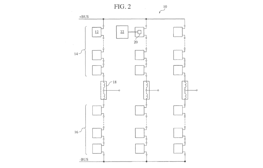
[0012] FIG. 2 illustrates various embodiments of an M2LC system;
[0013] FIG. 3 illustrates a representation of the dynamics of any given phase
of the M2LC system of FIG. 2;
[0014] FIG. 4 illustrates a 2nd order dynamical equation which describes the
response of an arm current of the M2LC system of FIG. 2;
- 4 -
CA 02866862 2014-09-09
WO 2013/134628
PCT/US2013/029845
[0015] FIGs. 5A and 5B illustrate high level representations of the
functionality of a system control module of the M2LC system of FIG. 2
according to
various embodiments; and
[0016] FIGs. 6A-9D illustrate results of simulations for a seven-level M2LC
system at various operating conditions.
DETAILED DESCRIPTION
[0017] It is to be understood that at least some of the figures and
descriptions
of the invention have been simplified to illustrate elements that are relevant
for a clear
understanding of the invention, while eliminating, for purposes of clarity,
other
elements that those of ordinary skill in the art will appreciate may also
comprise a
portion of the invention. However, because such elements are well known in the
art,
and because they do not facilitate a better understanding of the invention, a
description of such elements is not provided herein.
[0018] FIG. 2 illustrates various embodiments of an M2LC system 10 having
a plurality of M2LC cells 12. The M2LC system 10 is similar to the M2LC system
of
FIG. 1 in that the M2LC cells 12 are arranged as output phase modules, with
each
output phase module further arranged into a positive arm 14 and a negative arm
16,
and a given output phase module defines an inductance and a capacitance for
that
output phase module. However, as explained in more detail hereinafter, in
contrast to
the M2LC system of FIG. 1, the output phase modules are configured so that for
a
given output phase module, a natural resonant frequency of the inductance with
the
effective capacitance of the output phase module is greater than the operating
frequency of the output phase module, the switching frequency of the output
phase
module, and the switching frequency of any of the M2LC cells 12.
- 5 -
CA 02866862 2014-09-09
WO 2013/134628
PCT/US2013/029845
[0019] The inductance of a given output phase module may be realized
deterministically in any number of different ways. For example, according to
various
embodiments, the inductance may be realized deterministically by including a
deterministically sized inductive filter 18 between the positive and negative
arms 14,
16. Also, although the inductive filter 18 is shown as having two inductors
connected
between the positive and the negative arms 14, 16 of an output phase module,
it will
be appreciated that the inductive filter 18 may include any number of
inductors (e.g.,
one, two, three, four, etc.) connected between the positive and the negative
arms 14,
16 of an output phase module.
[0020] As further shown in FIG. 2, the M2LC system 10 may also include a
local control module 20 and a system control module 22. Although not shown for
purposes of simplicity, it will be appreciated that the local control module
20 is
communicably connected to the switching devices of the M2LC cell 12.
Furthermore,
although only one local control module 20 is shown in FIG. 2, it will be
appreciated
each of the M2LC cells 12 may include their own respective local control
modules 20.
The system control module 22 controls the M2LC cell switching functions and is
communicably connected to the local control module 20. For purposes of
simplicity,
the system control module 22 is shown in FIG. 2 as only being communicably
connected to one local control module 20. However, it will be appreciated that
the
M2LC system 10 may include a plurality of local control modules 20 and the
system
control module 22 may be communicably connected to the plurality of local
control
modules 20. The functionality of the system control module 22 will be
described in
more detail hereinbelow.
[0021] FIG. 3 illustrates a representation of the dynamics of any given phase
of the M2LC system 10 of FIG. 2. A current source (output current ioa) is
shown
- 6 -
CA 02866862 2014-09-09
WO 2013/134628
PCT/US2013/029845
connected to the output which causes current to flow from both the positive
and
negative arms. The dynamics of the resulting arm current (iarm) can be shown
to be a
function of this defined output current and the switching function of the M2LC
cells
12 can be shown to be influenced or filtered solely by the effective
inductance (L),
Resistance (R) and effective phase capacitance (C). In the case of the latter,
the
effective phase capacitance always looks like a constant when the capacitance
functions of each arm are summed. Stated differently, the effective phase
capacitance
for a given phase is equal to the following equation:
1
1 1
C(sap) +C (saN)
where saP is the sum of the switching functions of the positive arm and saN is
the
sum of the switching functions of the negative arm. It can thus be shown that
the
complete dynamics of the phase can be modeled using the 2nd order dynamical
equation shown in FIG. 4, where Isak is the arm current forcing function, the
state
variable ick represents the inductor current and fr is the resonance of the
phase or pole.
[0022] In view of FIG. 4, it will be appreciated that the resonant frequency
may be controlled by the selection of M2LC cell capacitance C and arm
inductance 1/2
L. As described in more detail hereinafter, by sizing the value of L to be
sufficiently
small so as to result in a resonant frequency greater than the switching
frequency of
the M2LC cells, certain modulation techniques may be utilized to cancel this
voltage
ripple at low output operating frequencies or alternatively allow the size of
the filter
capacitors to be reduced at normal operating frequencies. Additionally, with
this
approach, the use of large, costly, heavy iron/copper based inductors may be
eliminated in favor of small light weight powered iron based arm filters. The
trade-
- 7 -
CA 02866862 2014-09-09
WO 2013/134628
PCT/US2013/029845
off resulting in slightly higher rated switching devices to offset the
elevated arm
currents is a cost effective compromise with today's IGBT based switch
technology.
[0023] In view of the information associated with FIGs. 3 and 4, the size of
the inter-arm inductors should be sufficiently small in relation to the value
of the cell
filter capacitors so that the resonant frequency is sufficiently higher than
the desired
fundamental output frequency, the fundamental M2LC arm frequency, or the
switching frequency of the M2LC cells 12 which are modulated to develop the
desired output voltage and frequency of the M2LC system 10.
[0024] In further view of the information associated with FIGs. 3 and 4, the
method used to develop the common mode switching condition required to cancel
the
fundamental capacitor currents should be completely independent of the
reference
signals used to produce the desired output voltage waveform, and the degree of
this
cancellation can be controlled as required to limit the value of capacitor
ripple voltage
without effecting the fundamental output voltage value and significantly
effecting the
quality of the output voltage waveform.
[0025] As described in more detail hereinbelow, a system control module 22
of the M2LC system 10 may be utilized to control the degree of phase shift of
the
M2LC cell switching functions in the arm used to generate the required
fundamental
output voltage. As a result, the fundamental spectral component of each of the
M2LC
cell switching functions is essentially identical and independent of the
degree of phase
shift used to control the capacitor ripple voltage. Further, the non-
fundamental
spectral components of the M2LC cell switching functions are also essentially
identical except that they cancel in various degrees depending on the value of
phase
shift.
- 8 -
CA 02866862 2014-09-09
WO 2013/134628
PCT/US2013/029845
[0026] The system control module 22 may utilize either of two basic forms of
modulation to control the degree of phase shift of the M2LC cell switching
functions,
either multi-level sine/pulse width modulation (PWM) or multi-level Space
Vector.
The system control module 22 may be configured to modify either of these
modulation techniques to implement the phase shifting function described
hereinabove.
[0027] FIGs. 5A and 5B illustrate a high level representation of the
functionality of the system control module 22 of the M2LC system 10 according
to
various embodiments. The system control module 22 (or its functional
equivalent)
may be utilized to generate the desired M2LC cell switching functions. FIG. 5A
shows how a multi-level sine/PWM modulation technique may generate the M2LC
cell switching function to control capacitor voltage ripple and FIG. 5B shows
how a
multi-level space vector modulation technique may generate the M2LC cell
switching
function to control capacitor voltage ripple.
[0028] The system control module 22 may be implemented in hardware,
firmware, software and combinations thereof, and may reside at a higher level
controller (the hub controller) of the M2LC system 10. According to other
embodiments, the system control module 22 may be distributed amongst one or
more
of the local control modules 20 of the M2LC cells 12. For embodiments
utilizing
software, the software may utilize any suitable computer language (e.g., C,
C++, Java,
JavaScript, Visual Basic, VBScript, Delphi) and may be embodied permanently or
temporarily in any type of machine, component, physical or virtual equipment,
storage medium, or propagated signal capable of delivering instructions to a
device.
For embodiments where the system control module 22 is embodied as software
(e.g.,
software application, computer program), the software may be stored on a
computer-
- 9 -
CA 02866862 2014-09-09
WO 2013/134628
PCT/US2013/029845
readable medium (e.g., disk, device, and/or propagated signal) such that when
a
computer reads the medium, the functions described herein are performed.
[0029] In FIG. 5A, a classic multilevel PWM modulator is modified to control
the degree of phase shift between carrier waveforms using a simple scalar
function
(Omega) which can be controlled between the values 0 and 1. When Omega = 0,
the
multilevel modulator causes the M2LC cells to switch together like a classic
two-level
bridge. This produces the minimum value of capacitor voltage ripple in the
same way
a two-level bridge causes the fundamental current in its arms to cancel. When
Omega
= 1.0, optimum multilevel modulation is achieved if as shown the triangle
waveforms
are evenly spaced by the value of 211/N where N = 6 in this example. In this
case the
M2LC cell capacitors will produce a value of voltage ripple consistent with
the
operating frequency and output current level and no fundamental current
cancelation
in the M2LC cell capacitors occurs.
[0030] In practice, Omega may be controlled between 0.1 and 1Ø At 0.1
(used for DC starting or very low output frequency machine control),
significant
fundamental ripple voltage is cancelled (assuming that the resonant frequency
of the
arm is greater than the switching frequency). Even though significant common
mode
voltage is produced at the switching frequency of the M2LC cells 12, the
output
waveform still exhibits degrees of multilevel switching. In fact, even at
Omega = 0.1,
the dv/dt of the switches is the same as in the Omega = 1.0 condition.
[0031] In FIG. 5B, State Vector Modulation is utilized to control the degree
of
phase shift. In this case, a set of essentially identical M2LC cell switching
functions
are produced by computing the time average switch function which most closely
fits
the desired reference in the particular sample time.
- 10 -
CA 02866862 2014-09-09
WO 2013/134628
PCT/US2013/029845
[0032] Note that in either case, it is the act of phase shifting these M2LC
cell
switching functions which produces a "window" of time in which the output
terminal
controlled by the M2LC cells 12 is either completely connected to the positive
DC
bus and alternatively the negative DC bus. It is during these "windows" which
the
fundamental current component in the M2LC cell filter capacitors can be
canceled
assuming that the resonance frequency of the arm is greater than the cell
switching
frequency and hence the frequency of the "windows". Smaller time windows
(larger
values of Omega) are less effective in canceling the fundamental current in
the filter
capacitors of the M2LC cells 12 but a higher degree of output voltage waveform
is
achieved. It is in this way Omega can be varied depending on output
fundamental
frequency of the M2LC system 10 to both optimize capacitor voltage ripple and
output voltage quality (so called Harmonic Voltage Factor or HVF).
SIMULATIONS
[0033] Simulations were performed for a seven-level M2LC system (6
switching M2LC cells per arm) using the dynamic model described in FIG. 4.
Four
cases were simulated for the M2LC system operating at 30Hz (typical mid range
frequency), and an M2LC cell switching frequency of 600Hz, all operating at
rated
output current.
[0034] In first 3 simulations, the size of the inter-arm inductance (L) was
sized
with the M2LC cell filter capacitors so that the phase resonant frequency (fr)
is
approximately 1.5 times the switching frequency or about 900Hz. Phase shifts
produced by the modulation scheme depicted in FIG. 5A corresponding to Omega =
1.0, 0.5 and 0.1 were simulated. It will be appreciated that these conditions
could also
be developed in theory by the Space Vector scheme shown in FIG. 5B.
- 11 -
CA 02866862 2014-09-09
WO 2013/134628
PCT/US2013/029845
[0035] In a fourth simulation with Omega = 0.1, the phase inductance (L) was
increased to show that fundamental current cancelation is ineffective in
either
modulator technique (or any other common mode cancellation technique) unless
the
resonance of the phase is sufficiently greater than cell switching frequency
(fc) or the
resultant two-level window switching frequency of the phase.
SIMULATION 1
[0036] FIGs. 6A-6D show the results for the first simulation, where f3uir =
30Hz, fe = 600HZ, fr = 930HZ, and Omega = 1Ø As shown in these figures, the
M2LC cell switching functions (FIG. 6A) were essentially identical (same
fundamental and harmonics) but were optimally phase shifted to produce the
highest
quality output voltage (HVF = 0.028) and the fundamental value of the switch
functions was 1.179 (FIG. 6B). As shown in FIG. 6D, the filter capacitor
voltage
ripple was nearly 20% (1.183) of the average capacitor voltage.
SIMULATION 2
[0037] FIGs. 7A-7D show the results for the second simulation, where fc.r =
30Hz, fe = 600HZ, fr = 930HZ, and Omega = 0.5. As shown in these figures, the
M2LC cell switching functions (FIG. 7A) were still essentially identical but
phase
shift is reduced by 50%. The Harmonic Voltage Factor (FIG. 7B) actually
improved
but the fundamental value of the switch functions stayed the same. The filter
capacitor voltage ripple (FIG. 7D) was nearly 12% (1.117) or almost half the
value as
in Simulation 1.
[0038] Note the resonant nature of the arm current (iarm) in FIG. 7C in
relation to the arm voltage (VAarm) as compared to FIG. 6C. The fundamental
- 12 -
CA 02866862 2014-09-09
WO 2013/134628
PCT/US2013/029845
current was essentially canceling at the positive and negative DC busses of
the M2LC
system. The price here however was slightly higher peak currents in the
switches.
SIMULATION 3
[0039] FIGs. 8A-8D show the results for the third simulation, where tuir =
30Hz, fe = 600HZ, fr = 930HZ, and Omega = 0.1. As shown in these figures, the
M2LC cell switching functions (FIG. 8A) were reduced to 10%. The Harmonic
Voltage Factor (FIG. 8B) further improved but the fundamental value of the
switch
functions (FIG. 8B) stayed essentially the same as in the previous 2
simulations. The
filter capacitor voltage ripple (FIG. 8D) was only 5% of the cell capacitor
average
voltage. Note that this low level of output voltage ripple will occur down to
very low
output frequencies (even DC) at rated current.
SIMULATION 4
[0040] FIGs. 9A-9D show the results for the fourth simulation, where f3uir =
30Hz, fe = 600HZ, fr = 160HZ, and Omega = 0.1. For this simulation, the inter-
arm
inductance was increased to a value which caused the resonate frequency of the
phase
to be less than the cell switching frequency. Otherwise, Simulation 4 utilized
the
same operating condition utilized in Simulation 3. As shown in these figures,
the
fundamental capacitor current cancellation effect of the phase shifted cell
switching
functions (FIG. 9D) was completely eliminated when the phase resonate
frequency
became even slightly less than the phase window "+bus to ¨ bus" switching
frequency
which results from the M2LC cell switching period when the M2LC cell switch
functions are phase shifted. This was also evident by the fact that the arm
current in
FIG. 9C was no longer excited by the switching frequency as it was in FIG. 8C.
- 13 -
CA 02866862 2014-09-09
WO 2013/134628
PCT/US2013/029845
[0041] In view of the above, it will be appreciated that when utilized in
conjunction with the above-described modulation technique and the selection of
the
resonate frequency of the phase greater than the M2LC cell switching
frequency, the
M2LC system 10 is able to be utilized with synchronous machines under rated
torque
conditions.
[0042] Nothing in the above description is meant to limit the invention to any
specific materials, geometry, or orientation of elements. Many
part/orientation
substitutions are contemplated within the scope of the invention and will be
apparent
to those skilled in the art. The embodiments described herein were presented
by way
of example only and should not be used to limit the scope of the invention.
[0043] Although the invention has been described in terms of particular
embodiments in this application, one of ordinary skill in the art, in light of
the
teachings herein, can generate additional embodiments and modifications
without
departing from the spirit of, or exceeding the scope of, the claimed
invention.
Accordingly, it is understood that the drawings and the descriptions herein
are
proffered only to facilitate comprehension of the invention and should not be
construed to limit the scope thereof
- 14 -