Note: Descriptions are shown in the official language in which they were submitted.
CA 02866883 2014-09-09
WO 2013/136233 PCT/1B2013/051811
1
VECTOR FIND ELEMENT EQUAL INSTRUCTION
BACKGROUND
[0001] An aspect of the invention relates, in general, to text processing,
and in particular,
to facilitating processing associated with character data.
[0002] Text processing often requires the comparing of character data,
including, but not
limited to, the comparing of character data strings. Typically, instructions
used to compare
character data compare a single byte of data at a time.
[0003] Further, text processing often requires other types of string
processing, including
finding the termination point (e.g., end of a string), determining the length
of the character
data, finding a particular character, etc. Current instructions to perform
these types of
processing tend to be inefficient.
BRIEF SUMMARY
[0004] The shortcomings of the prior art are overcome and advantages are
provided
through the provision of a computer program product for executing a machine
instruction.
The computer program product includes a computer readable storage medium
readable by a
processing circuit and storing instructions for execution by the processing
circuit for
performing a method. The method includes, for instance, obtaining, by a
processor, a
machine instruction for execution, the machine instruction being defined for
computer
execution according to a computer architecture, the machine instruction
including, for
instance, at least one opcode field to provide an opcode, the opcode
identifying a Vector
Find Element Equal operation; an extension field to be used in designating one
or more
registers; a first register field combined with a first portion of the
extension field to designate
a first register, the first register including a first operand; a second
register field combined
with a second portion of the extension field to designate a second register,
the second
register including a second operand; a third register field combined with a
third portion of
the extension field to designate a third register, the third register
including a third operand; a
mask field, the mask field including one or more controls to be used during
execution of the
CA 02866883 2014-09-09
WO 2013/136233 PCT/1B2013/051811
2
machine instruction; and executing the machine instruction, the execution
including
determining whether the mask field includes a zero element control set to
indicate a search
for a zero element; based on the mask field including the zero element control
set to indicate
the search for a zero element, searching the second operand for a zero
element, the searching
providing a null index, the null index including one of an index of a zero
element found in
the search or an indication of no zero elements found; comparing one or more
elements of
the second operand with one or more elements of the third operand for
equality, the
comparing providing a compare index, the compare index including one of an
index of an
equal element based on the comparing finding an equal element or an indication
of no
equality based on the comparing finding no equal elements; providing a result,
the result
based on whether the search for zero element was performed, wherein the result
includes one
of: based on not performing the search for zero element, the result includes
the compare
index; or based on performing the search for zero element, the result includes
one of the
compare index or the null index.
[0005] Methods and systems relating to one or more aspects of the present
invention are
also described and claimed herein. Further, services relating to one or more
aspects of the
present invention are also described and may be claimed herein.
[0006] Additional features and advantages are realized through the
techniques of the
present invention. Other embodiments and aspects of the invention are
described in detail
herein and are considered a part of the claimed invention.
BRIEF DESCRIPTION OF THE SEVERAL VIEWS OF THE DRAWINGS
[0007] One or more aspects of the present invention are particularly
pointed out and
distinctly claimed as examples in the claims at the conclusion of the
specification. The
foregoing and other objects, features, and advantages of the invention are
apparent from the
following detailed description taken in conjunction with the accompanying
drawings in
which:
FIG. 1 depicts one example of a computing environment to incorporate and use
one or more
aspects of the present invention;
CA 02866883 2014-09-09
WO 2013/136233 PCT/1B2013/051811
3
FIG. 2A depicts another example of a computing environment to incorporate and
use one or
more aspects of the present invention;
FIG. 2B depicts further details of the memory of FIG. 2A, in accordance with
an aspect of
the present invention;
FIG. 3 depicts one embodiment of a format of a Vector Find Element Equal
instruction, in
accordance with an aspect of the present invention;
FIG. 4 depicts one embodiment of the logic associated with a Vector Find
Element Equal
instruction, in accordance with an aspect of the present invention;
FIG. 5 depicts one embodiment of various processing blocks to perform the
logic of FIG. 4,
in accordance with an aspect of the present invention;
FIG. 6 depicts one example of a register field, in accordance with an aspect
of the present
invention;
FIG. 7 depicts one embodiment of a format of a Vector Find Any Equal
instruction, in
accordance with an aspect of the present invention;
FIG. 8 depicts one embodiment of the logic associated with a Vector Find Any
Equal
instruction, in accordance with an aspect of the present invention;
FIG. 9 depicts one embodiment of a computer program product incorporating one
or more
aspects of the present invention;
FIG. 10 depicts one embodiment of a host computer system to incorporate and
use
one or more aspects of the present invention;
FIG. 11 depicts a further example of a computer system to incorporate and use
one or
more aspects of the present invention;
FIG. 12 depicts another example of a computer system comprising a computer
network to incorporate and use one or more aspects of the present invention;
CA 02866883 2014-09-09
WO 2013/136233 PCT/1B2013/051811
4
FIG. 13 depicts one embodiment of various elements of a computer system to
incorporate and use one or more aspects of the present invention;
FIG. 14A depicts one embodiment of the execution unit of the computer system
of
FIG. 13 to incorporate and use one or more aspects of the present invention;
FIG. 14B depicts one embodiment of the branch unit of the computer system of
FIG.
13 to incorporate and use one or more aspects of the present invention;
FIG. 14C depicts one embodiment of the load/store unit of the computer system
of
FIG. 13 to incorporate and use one or more aspects of the present invention;
and
FIG. 15 depicts one embodiment of an emulated host computer system to
incorporate and
use one or more aspects of the present invention.
DETAILED DESCRIPTION
[0008] In accordance with an aspect of the present invention, a capability
is provided for
facilitating processing of character data, including, but not limited to,
alphabetic characters,
in any language; numeric digits; punctuation; and/or other symbols. The
character data may
or may not be strings of data. Associated with character data are standards,
examples of
which include, but are not limited to, ASCII (American Standard Code for
Information
Interchange); Unicode, including, but not limited to, UTF (Unicode
Transformation Format)
8; UTF16; etc.
[0009] In one example, a Find Element Equal instruction is provided that
compares data
of multiple vectors for equality and provides an indication of equality, if
equality exists. In
one example, an index associated with the equal element is stored in a target
vector register.
[0010] As described herein, an element of a vector register (also referred
to as a vector)
is one, two or four bytes in length, as examples; and a vector operand is, for
instance, a
SIMD (Single Instruction, Multiple Data) operand having a plurality of
elements. In other
embodiments, elements can be of other sizes; and a vector operand need not be
SIMD,
and/or may include one element.
CA 02866883 2014-09-09
WO 2013/136233 PCT/1B2013/051811
[0011] In a further embodiment, the same instruction, the Find Element
Equal
instruction, also searches a selected vector for null elements, also referred
to as zero
elements (e.g., entire element is zero). A null or zero element indicates
termination of the
character data; e.g., an end of a particular string of data. A result of the
instruction is
dependent on whether the null search is provided, or just the compare.
[0012] In yet a further embodiment, a Vector Find Any Equal instruction is
provided that
searches a vector for particular characters and/or for zero elements, and
returns a mask or
byte index of the matched character or zero element.
[0013] One embodiment of a computing environment to incorporate and use one
or more
aspects of the present invention is described with reference to FIG. 1. A
computing
environment 100 includes, for instance, a processor 102 (e.g., a central
processing unit), a
memory 104 (e.g., main memory), and one or more input/output (I/O) devices
and/or
interfaces 106 coupled to one another via, for example, one or more buses 108
and/or other
connections.
[0014] In one example, processor 102 is based on the z/Architecture offered
by
International Business Machines Corporation, and is part of a server, such as
the System z
server, which is also offered by International Business Machines Corporation
and
implements the z/Architecture. One embodiment of the z/Architecture is
described in an
IBM publication entitled, "z/Architecture Principles of Operation," IBM
Publication No.
5A22-7832-08, Ninth Edition, August, 2010. In one example, the processor
executes an
operating system, such as z/OS, also offered by International Business
Machines
Corporation. IBM , Z/ARCHITECTURE and Z/OS are registered trademarks of
International Business Machines Corporation, Armonk, New York, USA. Other
names used
herein may be registered trademarks, trademarks, or product names of
International Business
Machines Corporation or other companies.
[0015] In a further embodiment, processor 102 is based on the Power
Architecture
offered by International Business Machines Corporation. One embodiment of the
Power
Architecture is described in "Power ISATM Version 2.06 Revision B,"
International Business
Machines Corporation, July 23, 2010. POWER ARCHITECTURE is a registered
trademark of International Business Machines Corporation.
CA 02866883 2014-09-09
WO 2013/136233 PCT/1B2013/051811
6
[0016] In yet a further embodiment, processor 102 is based on an Intel
architecture
offered by Intel Corporation. One embodiment of the Intel architecture is
described in
"Intel 64 and IA-32 Architectures Developer's Manual: Vol. 2B, Instructions
Set
Reference, A-L," Order Number 253666-041U5, December 2011, and "Intel 64 and
IA-32
Architectures Developer's Manual: Vol. 2B, Instructions Set Reference, M-Z,"
Order
Number 253667-041U5, December 2011. Intel is a registered trademark of Intel
Corporation, Santa Clara, California.
[0017] Another embodiment of a computing environment to incorporate and use
one or
more aspects of the present invention is described with reference to FIG. 2A.
In this
example, a computing environment 200 includes, for instance, a native central
processing
unit 202, a memory 204, and one or more input/output devices and/or interfaces
206 coupled
to one another via, for example, one or more buses 208 and/or other
connections. As
examples, computing environment 200 may include a PowerPC processor, a pSeries
server
or an xSeries server offered by International Business Machines Corporation,
Armonk, New
York; an HP Superdome with Intel Itanium II processors offered by Hewlett
Packard Co.,
Palo Alto, California; and/or other machines based on architectures offered by
International
Business Machines Corporation, Hewlett Packard, Intel, Oracle, or others.
[0018] Native central processing unit 202 includes one or more native
registers 210, such
as one or more general purpose registers and/or one or more special purpose
registers used
during processing within the environment. These registers include information
that
represent the state of the environment at any particular point in time.
[0019] Moreover, native central processing unit 202 executes instructions
and code that
are stored in memory 204. In one particular example, the central processing
unit executes
emulator code 212 stored in memory 204. This code enables the processing
environment
configured in one architecture to emulate another architecture. For instance,
emulator code
212 allows machines based on architectures other than the z/Architecture, such
as PowerPC
processors, pSeries servers, xSeries servers, HP Superdome servers or others,
to emulate the
z/Architecture and to execute software and instructions developed based on the
z/Architecture.
CA 02866883 2014-09-09
WO 2013/136233 PCT/1B2013/051811
7
[0020] Further details relating to emulator code 212 are described with
reference to FIG.
2B. Guest instructions 250 comprise software instructions (e.g., machine
instructions) that
were developed to be executed in an architecture other than that of native CPU
202. For
example, guest instructions 250 may have been designed to execute on a
z/Architecture
processor 102, but instead, are being emulated on native CPU 202, which may
be, for
example, an Intel Itanium II processor. In one example, emulator code 212
includes an
instruction fetching unit 252 to obtain one or more guest instructions 250
from memory 204,
and to optionally provide local buffering for the instructions obtained. It
also includes an
instruction translation routine 254 to determine the type of guest instruction
that has been
obtained and to translate the guest instruction into one or more corresponding
native
instructions 256. This translation includes, for instance, identifying the
function to be
performed by the guest instruction and choosing the native instruction(s) to
perform that
function.
[0021] Further, emulator 212 includes an emulation control routine 260 to
cause the
native instructions to be executed. Emulation control routine 260 may cause
native CPU 202
to execute a routine of native instructions that emulate one or more
previously obtained
guest instructions and, at the conclusion of such execution, return control to
the instruction
fetch routine to emulate the obtaining of the next guest instruction or a
group of guest
instructions. Execution of the native instructions 256 may include loading
data into a
register from memory 204; storing data back to memory from a register; or
performing some
type of arithmetic or logic operation, as determined by the translation
routine.
[0022] Each routine is, for instance, implemented in software, which is
stored in memory
and executed by native central processing unit 202. In other examples, one or
more of the
routines or operations are implemented in firmware, hardware, software or some
combination thereof The registers of the emulated processor may be emulated
using
registers 210 of the native CPU or by using locations in memory 204. In
embodiments,
guest instructions 250, native instructions 256 and emulator code 212 may
reside in the same
memory or may be disbursed among different memory devices.
[0023] As used herein, firmware includes, e.g., the microcode, millicode
and/or
macrocode of the processor. It includes, for instance, the hardware-level
instructions and/or
data structures used in implementation of higher level machine code. In one
embodiment, it
CA 02866883 2014-09-09
WO 2013/136233 PCT/1B2013/051811
8
includes, for instance, proprietary code that is typically delivered as
microcode that includes
trusted software or microcode specific to the underlying hardware and controls
operating
system access to the system hardware.
[0024] In one example, a guest instruction 250 that is obtained, translated
and executed
is one of the instructions described herein. The instruction, which is of one
architecture
(e.g., the z/Architecture) is fetched from memory, translated and represented
as a sequence
of native instructions 256 of another architecture (e.g., PowerPC, pSeries,
xSeries, Intel,
etc.). These native instructions are then executed.
[0025] In one embodiment, the instructions described herein are vector
instructions,
which are part of a vector facility, provided in accordance with an aspect of
the present
invention. The vector facility provides, for instance, fixed sized vectors
ranging from one to
sixteen elements. Each vector includes data which is operated on by vector
instructions
defined in the facility. In one embodiment, if a vector is made up of multiple
elements, then
each element is processed in parallel with the other elements. Instruction
completion does
not occur until processing of all the elements is complete.
[0026] As described herein, the vector instructions can be implemented as
part of various
architectures, including, but not limited to, the z/Architecture, Power,
Intel, etc. Although an
embodiment described herein is for the z/Architecture, the vector instructions
and one or
more aspects of the present invention may be based on many other
architectures. The
z/Architecture is only one example.
[0027] In one embodiment in which the vector facility is implemented as
part of the
z/Architecture, to use the vector registers and instructions, a vector
enablement control and a
register control in a specified control register (e.g., control register 0)
are set to, for instance,
one. If the vector facility is installed and a vector instruction is executed
without the
enablement controls set, a data exception is recognized. If the vector
facility is not installed
and a vector instruction is executed, an operation exception is recognized.
[0028] Vector data appears in storage, for instance, in the same left-to-
right sequence as
other data formats. Bits of a data format that are numbered 0-7 constitute the
byte in the
leftmost (lowest-numbered) byte location in storage, bits 8-15 form the byte
in the next
CA 02866883 2014-09-09
WO 2013/136233 PCT/1B2013/051811
9
sequential location, and so on. In a further example, the vector data may
appear in storage in
another sequence, such as right-to-left.
[0029] Many of the vector instructions provided with the vector facility
have a field of
specified bits. This field, referred to as the register extension bit or RXB,
includes the most
significant bit for each of the vector register designated operands. Bits for
register
designations not specified by the instruction are to be reserved and set to
zero.
[0030] In one example, the RXB field includes four bits (e.g., bits 0-3),
and the bits are
defined, as follows:
[0031] 0 - Most significant bit for the first vector register designation
of the instruction.
[0032] 1 - Most significant bit for the second vector register designation
of the
instruction, if any.
[0033] 2 - Most significant bit for the third vector register designation
of the instruction,
if any.
[0034] 3 - Most significant bit for the fourth vector register designation
of the
instruction, if any.
[0035] Each bit is set to zero or one by, for instance, the assembler
depending on the
register number. For instance, for registers 0-15, the bit is set to 0; for
registers 16-31, the
bit is set to 1, etc.
[0036] In one embodiment, each RXB bit is an extension bit for a particular
location in
an instruction that includes one or more vector registers. For instance, in
one or more vector
instructions, bit 0 of RXB is an extension bit for location 8-11, which is
assigned to, e.g., Vi;
bit 1 of RXB is an extension bit for location 12-15, which is assigned to,
e.g., V2; and so
forth.
[0037] In a further embodiment, the RXB field includes additional bits, and
more than
one bit is used as an extension for each vector or location.
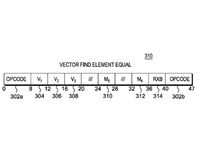
[0038] One instruction, provided in accordance with an aspect of the
present invention
that includes the RXB field is a Vector Find Element Equal instruction, an
example of which
CA 02866883 2014-09-09
WO 2013/136233 PCT/1B2013/051811
is depicted in FIG. 3. In one example, the Vector Find Element Equal
instruction 300
includes opcode fields 302a (e.g., bits 0-7), 302b (e.g., bits 40-47)
indicating a Vector Find
Element Equal operation; a first vector register field 304 (e.g., bits 8-11)
used to designate a
first vector register (Vi); a second vector register field 306 (e.g., bits 12-
15) used to
designate a second vector register (V2); a third vector register field 308
(e.g., bits 16-19)
used to designate a third vector register (V3); a first mask field (M5) 310
(e.g., bits 24-27); a
second mask field (M4) 312 (e.g., bits 32-35); and an RXB field 314 (e.g.,
bits 36-39). Each
of the fields 304-314, in one example, is separate and independent from the
opcode field(s).
Further, in one embodiment, they are separate and independent from one
another; however,
in other embodiments, more than one field may be combined. Further information
on the
use of these fields is described below.
[0039] In one example, selected bits (e.g., the first two bits) of the
opcode designated by
opcode field 302a specify the length and format of the instruction. In this
particular
example, the selected bits indicate that the length is three halfwords and the
format is a
vector register-and register operation with an extended opcode. Each of the
vector (V)
fields, along with its corresponding register extension bit specified by RXB,
designates a
vector register. In particular, for vector registers, the register containing
the operand is
specified using, for instance, a four-bit field of the register field with the
addition of the
register extension bit (RXB) as the most significant bit. For instance, if the
four bit field is
0110 and the extension bit is 0, then the five bit field 00110 indicates
register number 6.
[0040] The subscript number associated with a field of the instruction
denotes the
operand to which the field applies. For instance, the subscript number 1
associated with
vector register Vi denotes the first operand, and so forth. A register operand
is one register
in length, which is, for instance, 128 bits.
[0041] The M4 field having, for instance, four bits, 0-3, specifies an
element size control
in, for instance, bits 1-3. The element size control specifies the size of the
elements in the
vector register operands. As examples, the element size control specifies
either a byte,
halfword (e.g., 2 bytes) or word (e.g., 4 bytes). For instance, a 0 indicates
a byte; a 1
indicates a halfword; and a 2 indicates a word, a.k.a., fullword. If a
reserved value is
specified, a specification exception is recognized.
CA 02866883 2014-09-09
WO 2013/136233 PCT/1B2013/051811
11
[0042] The M5 field, is, for instance, a four bit field, bits 0-3,
including, for instance:
[0043] A zero search field (ZS, bit 2), which if one, each element of the
second
operand is compared to zero (or null). (In a further example, it is each
element of the third operand or another operand that is compared to zero); and
[0044] A condition code set field (CC, bit 3), which if zero, the
condition code is not
set and remains unchanged. If one, the condition code is set as specified
below, as an example:
[0045] 0 - If the zero search bit is set, comparison detected a
zero element in
the second operand in an element with a smaller index than any
equal comparisons.
[0046] 1 - Comparison detected a match between the second and third
operands in some element. If the zero search bit is set, this match
occurred in an element with an index less than or equal to the zero
comparing element.
[0047] 2 - ¨
[0048] 3 - No element compared equal.
[0049] In execution of one embodiment of the Vector Find Element Equal
instruction,
proceeding in one embodiment from left to right, the unsigned binary integer
elements of the
second operand (included within the register designated by V2 plus its RXB
bit) are
compared with the corresponding unsigned binary integer elements of the third
operand
(included within the register designated by V3 plus its RXB bit). If two
elements are equal, a
byte index of the first byte of the leftmost equal element is placed in a
selected byte (e.g.,
byte 7) of the first operand (included within a register designated by V1 plus
its RXB bit).
Zeros are stored in the remaining bytes of the first operand.
[0050] For instance, if the element size is one byte, then the byte index
of the leftmost
equal element is returned (e.g., if there are 16 elements, 0-15, and element 6
is equal, then
byte index 6 is returned). Similarly, if the element size is halfword, and
there are 8 elements,
0-7, and both byte 6 or 7 of element three is equal, then byte index 6 is
returned. Likewise,
CA 02866883 2014-09-09
WO 2013/136233 PCT/1B2013/051811
12
if the element size is fullword and there are four elements, 0-3, and all of
bytes 4-7 of
element one is equal, byte index 4 is returned.
[0051] If no bytes are found to be equal, or zero if the zero search is
set, then an index
equal to the vector size (e.g., number of bytes; e.g., 16) is stored in the
specified byte (e.g.,
byte 7) of the first operand. Zeros are stored in the remaining bytes.
[0052] If the zero search bit is set in the M5 field, then each element in
the second
operand (or in another embodiment, another operand, such as operand three) is
also
compared for equality with zero (or null; end of string). If a zero element is
found in the
second operand before any other elements of the second and third operands are
found to be
equal, the byte index of the first byte of the element found to be zero is
stored in the
specified byte (e.g., byte 7) of the first operand and zeros are stored in all
other byte
locations. If the condition code set flag is one, then the condition code is
set to zero.
[0053] In one embodiment, the comparison of the elements is performed in
parallel. For
instance, if the vector registers being compared are 16 bytes in length, then
16 bytes are
compared in parallel. Further, in one embodiment, the direction of the
vectors, left-to-right
or right-to-left, is provided at runtime. For instance, the instruction
accesses a register,
status control or other entity that indicates the direction of processing as
either left-to-right
or right-to-left, as examples. In one embodiment, this direction control is
not encoded as
part of the instruction, but provided to the instruction at runtime.
[0054] In a further embodiment, the instruction does not include the RXB
field. Instead,
no extension is used or the extension is provided in another manner, such as
from a control
outside of the instruction, or provided as part of another field of the
instruction.
[0055] Further details regarding one embodiment of processing the Vector
Find Element
Equal instruction are described with reference to FIG. 4. In one example, a
processor of the
computing environment is performing this logic.
[0056] Initially, a determination is made as to whether a search for null
(a.k.a., zero
element, end of string, terminator, etc.) is to be performed, INQUIRY 400. If
a search for
null is to be performed, a comparison is made against null characters, i.e.,
for zero elements,
STEP 402, and the result is output to nullidx 403. For instance, if the
element size is bytes
CA 02866883 2014-09-09
WO 2013/136233 PCT/1B2013/051811
13
and a zero element is found in byte 5, the index of the byte in which the zero
element is
found (e.g., 5) is placed in nullidx. Similarly, if the element size is
halfword, and there are 8
elements, 0-7, and element three (i.e., bytes 6-7) is zero, then 6 (for byte
index 6) is placed in
nullidx. Likewise, if the element size is fullword and there are four
elements, 0-3, and
element one (i.e., bytes 4-7) is zero, then 4 (for byte index 4) is placed in
nullidx. If no null
element is found, then, in one example, the size of the vector (e.g., in
bytes; e.g., 16) is
placed in nullidx.
[0057] Additionally, or if no null search is to be performed, a plurality
of comparisons
(e.g., 16) are performed in parallel comparing A to B based on a compare
operation, STEP
404. In one example, A is the contents of the second operand and B is the
contents of the
third operand, and the compare operation is equal.
[0058] A result of the compare is stored in a variable 406, referred to
either as a left
index, cmpidxl, or a right index, cmpidxr, depending on whether the search is
from the left
or the right. For instance, if the comparison is an equal comparison, the
search is left-to-
right, and the comparison results in one or more equalities, the index
associated with the first
byte of the lowest equal element is placed in cmpidxl. As one example, if the
element size is
bytes and there are 16 elements in the vector (0-15) and an equality is found
in element 6,
then 6 is stored in cmpidxl. Similarly, if the element size is halfwords, and
there are 8
elements in the vector (0-7), and an equality is found in element 3 (e.g., at
byte 6 or 7), the
index of the first byte of the element (byte 6) is returned. Likewise, if the
element size is
fullword and there are four elements (0-3), and an equality is found in
element 1 (e.g., at
byte 4-7), the index of the first byte of the element (byte 4) is returned. If
there are no equal
comparisons, then, in one embodiment, cmpidxl or cmpidxr, depending on
direction of the
compare, is set equal to the size of the vector (e.g., in bytes; e.g., 16).
[0059] Thereafter, a determination is made as to whether the search is from
the left or
right, INQUIRY 408. If the search is from the left, a variable cmpidx is set
equal to
cmpidxl, STEP 410; otherwise, cmpidx is set equal to cmpidxr, STEP 412.
[0060] Subsequent to setting cmpidx, a determination is made as to whether
a search was
performed for null characters, INQUIRY 414. If there was no search for null
characters,
then a variable, idx, is set, for instance, or the compare index, cmpidx, STEP
416. If null
CA 02866883 2014-09-09
WO 2013/136233 PCT/1B2013/051811
14
was searched, then idx is set to the minimum of the compare index or the null
index, nullidx,
STEP 418. This concludes processing.
[0061] An example of block logic for the processing of FIG. 4 is depicted
in FIG. 5. In
this example, there are two inputs, Vector B 500 and Vector A 502. Both inputs
are input to
comparison logic 504, which performs the comparisons (e.g., equal) in
parallel. Further, one
input, Vector A, is also input to zero detection logic 506, which performs
null processing.
[0062] The output of the comparison logic, idxL or idxR 508, is input to
result
determination logic 512, as well as the output of the zero detection logic,
nullidx 510. The
result determination logic also takes as input the following controls:
right/left 514 indicating
the direction of the search; zero detect 516 indicating whether null
processing is to be
performed; and element size 518 providing the size of each element (e.g.,
byte, halfword,
word); and produces a resulting index 520, resultidx, which is stored in an
output vector 522
(e.g., in byte 7).
[0063] Further, the result determination logic includes condition code
processing 523,
which optionally outputs a condition code 524.
[0064] Example pseudo-code for comparison logic 504 is as follows:
[0065] idxL = 16; idxR = 16
[0066] For i = 0 to vector length
[0067] If A[i] = to B[i] THEN
[0068] idxL = i
[0069] Done
[0070] For i = vector length downto 0
[0071] If A[i] = to B[i] THEN
[0072] idxR = i
[0073] done
CA 02866883 2014-09-09
WO 2013/136233 PCT/1B2013/051811
[0074] As shown, variable idxL or idxR, depending on direction, is
initialized to the size
of the vector (e.g., in number of bytes; e.g., 16). Then, each element of
Vector A is
compared to a corresponding element of Vector B. In one example, the
comparisons are
byte comparisons, so a comparison is made for each of the 16 bytes (i). In
this example, the
comparison operation is equal, and if an equality is found, the index of the
byte is stored in
idxL if searching from left, or idxR if searching from right.
[0075] Example pseudo-code for zero detection logic 506 is as follows:
[0076] nullidx = 16
[0077] FOR j = 0 to vector length
[0078] IF AU] ¨ 0 THEN
[0079] nullidx = j x element size
[0080] Done
[0081] As shown, each element (j) of the vector is tested to see if it is
equal to zero. If
an element is equal to zero, nullidx is set equal to the index of that element
times the element
size. For instance, if the element size if halfwords (2 bytes), and a null
character is detected
in element 3, 3 is multiplied by 2, and nullidx is set to 6, which represents
byte 6. Similarly,
if the element size is fullword (4 bytes), and a null character is detected in
element 3, 3 is
multiplied by 4, and nullidx is set to 12.
[0082] Likewise, example pseudo-code for result determination logic 512 is
as follows:
[0083] IF Left/Right = Left THEN
[0084] cmpidx = idxL
[0085] ELSE
[0086] cmpidx = idxR
[0087] IF zero detect = ON THEN
CA 02866883 2014-09-09
WO 2013/136233 PCT/1B2013/051811
16
[0088] resultidx = min(cmpidx, nullidx)
[0089] IF set CC = ON && nulldix<=cmpidx THEN
[0090] CC = 0
[0091] ELSE
[0092] resultidx = cmpidx
[0093] IF element size = byte THEN element size mask = `11111'b
[0094] IF element size = 2byte THEN element size mask = '11110'b
[0095] IF element size = 4byte THEN element size mask = '11100'b
[0096] resultidx = resultidx & element size mask
[0097] IF SetCC = ON THEN
[0098] IF nullidx < cmpidx THEN
[0099] CC = 0
[00100] ELSE IF cmpidx < 16 THEN
[00101] CC = 1
[00102] ELSE
[00103] CC = 3
[00104] As shown, if the left/right control indicates left, then cmpidx is set
equal to idxL;
otherwise, cmpidx is set equal to idxR. Further, if the zero detect indicator
is on, then
resultidx is set equal to the minimum of cmpidx or nullidx; and if the
condition code set
control is on and cmpidx is greater than nullidx, the condition code is set to
zero. Otherwise,
if zero detect is not on, resultidx is set equal to cmpidx.
CA 02866883 2014-09-09
WO 2013/136233 PCT/1B2013/051811
17
[00105] Further, if element size is equal to byte, then an element size mask
is set to
1111111; if element size is equal to 2 bytes, the mask is set to 1111101, and
if element size is
equal to 4 bytes, the mask is set to 1111001.
[00106] Thereafter, resultidx is set equal to resultidx ANDed with element
size mask. For
instance, if element size is halfword and byte 7 is resultidx, then resultidx
= 00111 AND
11110, providing 00110; so resultidx is set equal to 6 (i.e., 00110 in
binary), which is the
first byte of the element.
[00107] Additionally, a condition code is optionally set. If the set condition
code control
of the instruction is set on, then a condition code is provided; otherwise, no
condition code is
set. As examples, if the control is set on, then if nullidx < cmpidx, the
condition code is set
to 0. Otherwise, if cmpidx < 16, then the condition code is set to 1; else,
the condition code
is set to 3.
[00108] Described above is one example of a vector instruction used to
facilitate character
data processing. As described herein, for a 128 bit vector, the comparison
logic only
performs 16 byte compares, rather than, for instance, 256 compares. This
provides for
scaling for larger vectors. Further, a left/right control may be provided as a
runtime value
and not encoded within the instruction. Yet further, the value returned as the
result is a byte
position, rather than an element index. Further, 4 byte compares along with 1
byte and 2
byte compares are supported.
[00109] In one embodiment, there are 32 vector registers and other types of
registers can
map to a quadrant of the vector registers. For instance, as shown in FIG. 6,
if there is a
register file 600 that includes 32 vector registers 602 and each register is
128 bits in length,
then 16 floating point registers 604, which are 64 bits in length, can overlay
the vector
registers. Thus, as an example, when floating point register 2 is modified,
then vector
register 2 is also modified. Other mappings for other types of registers is
also possible.
[00110] In a further aspect of the invention, another instruction provided
with the vector
facility and used in accordance with an aspect of the present invention is a
Vector Find Any
Equal instruction, in which all characters (or a subset in another embodiment)
in an input
vector are compared to each character (or selected characters) in another
input vector.
Output is recorded either as a mask or an index to a character that matched.
This is useful,
CA 02866883 2014-09-09
WO 2013/136233 PCT/1B2013/051811
18
for instance, when parsing character data, such as strings of data. When
parsing, one
operation that is performed is to look for several special characters before
proceeding to the
next parsing step. This instruction enables searching for several characters
at once.
[00111] An example of the Vector Find Any Equal instruction is depicted in
FIG. 7, in
which in one embodiment, a Vector Find Any Equal instruction 700 includes, for
instance,
opcode fields 702a (e.g., bits 0-7), 702b (e.g., bits 40-47) indicating a
Vector Find Any
Equal operation; a first vector register field 704 (e.g., bits 8-11) used to
designate a first
vector register (Vi); a second vector register field 706 (e.g., bits 12-15)
used to designate a
second vector register (V2); a third vector register field 708 (e.g., bits 16-
19) used to
designate a third vector register (V3); a first mask field (M5) 710 (e.g.,
bits 24-27); a second
mask field (M4) (e.g., bits 32-35) 712; and an RXB field 714 (e.g., bits 36-
39). Each of the
fields 704-714, in one example, is separate and independent from the opcode
field(s).
Further, in one embodiment, they are separate and independent from one
another; however,
in other embodiments, more than one field may be combined. Further information
on the
use of these fields is described below.
[00112] Similar to above, in this example, selected bits (e.g., the first
two bits) of the
opcode designated by opcode field 702a specify the length and format of the
instruction. In
this example, the selected bits indicate that the length is three halfwords
and the format is a
vector register ¨ and register operation with an extended opcode field. Each
of the vector
(V) fields, along with its corresponding extension bit specified by RXB,
designates a vector
register. In particular, for vector registers, the register containing the
operand is specified
using, for instance, a four-bit field of the register field with the addition
of the register
extension bit (RXB) as the most significant bit. For instance, if the four bit
field is 0110 and
the extension bit is 0, then the five bit field 00110 indicates register
number 6.
[00113] The subscript number associated with a field of the instruction
denotes the
operand to which the field applies. For instance, the subscript number 1
associated with
vector register Vi denotes the first operand, and so forth. A register operand
is one register
in length, which is, for instance, 128 bits.
[00114] The M4 field having, for instance, four bits, 0-3, specifies the
element size control
in, for instance, bits 1-3. The element size control specifies the size of the
elements in the
CA 02866883 2014-09-09
WO 2013/136233
PCT/1B2013/051811
19
vector register operands. In one example, the element size control specifies a
byte, halfword
(e.g., 2 bytes) or word (e.g., 4 bytes). For instance, a 0 indicates a byte; a
1 indicates a
halfword; and a 2 indicates a word, a.k.a., a fullword. If a reserved value is
specified, a
specification exception is recognized.
[00115] The M5
field is, for instance, a four bit field, bits 0-3, including, for instance:
[00116] A result type field (RT, bit 1), which if zero, each resulting
element is a mask
of all range comparisons on that element. If one, a byte index is stored into
a
specified byte (e.g., byte 7) of the first operand and zeros are stored in all
other elements;
[00117] A zero search field (ZS, bit 2), which if one, each element of the
second
operand (or another operand) is compared to zero; and
[00118] A condition code set field (CC, bit 3), which if zero, the
condition code is not
set and remains unchanged. If one, the condition code is set as follows, in
one example:
[00119] 0 ¨ If the zero search bit is set, there were no matches in a
lower index
element than zero in the second operand.
[00120] 1 ¨ Some elements of the second operand match at least one
element in
the third operand;
[00121] 2 ¨ All elements of the second operand match at least one
element in the
third operand; and
[00122] 3 ¨ No elements of the second operand match any elements in the
third
operand.
[00123] In execution of one embodiment of the Vector Find Any Equal
instruction,
proceeding, in one example, from left to right, every unsigned binary integer
element of the
second operand (included within a register designated by V2 plus RXB) is
compared for
equality with each unsigned binary integer element of the third operand
(included within a
CA 02866883 2014-09-09
WO 2013/136233 PCT/1B2013/051811
register designated by V3 plus RXB) and optionally, zero, if the zero search
flag is set in the
M5 field.
[00124] If the result type flag in the M5 field is zero, then for each element
in the second
operand that matches any element in the third operand, or optionally zero, the
bit positions of
the corresponding element in the first operand (included within a register
designated by V1
plus RXB) are set to ones; otherwise, they are set to zero.
[00125] If the result type flag in the M5 field is one, then a byte index of
the leftmost
element (e.g., a byte index of the first byte of the element) in the second
operand that
matches an element in the third operand or zero is stored in the specified
byte (e.g., byte 7)
of the first operand.
[00126] If the result type flag in the M5 field is one and no bytes are found
to be equal, or
zero if the zero search flag is set, then an index equal to the size of the
vector (e.g., number
of bytes; e.g., 16) is stored in the specified byte (e.g., byte 7) of the
first operand.
[00127] In one embodiment, the direction of the vectors, left-to-right or
right-to-left, is
provided at runtime. For instance, the instruction accesses a register, status
control or other
entity that indicates the direction of processing as either left-to-right or
right-to-left, as
examples. In one embodiment, this direction control is not encoded as part of
the
instruction, but provided to the instruction at runtime.
[00128] In a further embodiment, the instruction does not include the RXB
field. Instead,
no extension is used or the extension is provided in another manner, such as
from a control
outside of the instruction, or provided as part of another field of the
instruction.
[00129] Further details regarding one embodiment of the Vector Find Any Equal
instruction are described with reference to FIG. 8. In one example, a
processor of the
computing environment is performing this logic.
[00130] Initially, variables referred to as zeroidx 802, resultidx 804 and
resultmask 806
are initialized, STEP 800. For instance, zeroidx is set equal to the size of
the second operand
(e.g., 16); resultidx is set equal to the size of the second operand (e.g.,
16); and resultmask is
CA 02866883 2014-09-09
WO 2013/136233 PCT/1B2013/051811
21
set equal to all zeros. Resultmask, in one embodiment, includes 128 bits
corresponding to
the 128 bits of the second operand.
[00131] Thereafter, a character (i.e., an element) is loaded from an
operand, referred to
herein as opA, which is, for instance, the second operand of the instruction,
STEP 808.
Thereafter, a determination is made as to whether the zero search field is set
indicating a
zero search and zeroidx is set equal to 16, INQUIRY 810. If so, a zero search
is performed,
STEP 812, and the result is output to zeroidx 802 and resultmask 806. For
instance, a byte
index of the leftmost byte of the zero element is indicated in zeroidx, and
the bits
corresponding to that element in resultmask are set to one. For instance, for
zeroidx, if the
element size is bytes and a zero element is found in byte 5, the index of the
byte in which the
zero element is found (e.g., 5) is placed in zeroidx. Similarly, if the
element size is
halfword, and there are 8 elements, 0-7, and element three (i.e., bytes 6-7)
is zero, then 6 (for
byte index 6) is placed in zeroidx. Likewise, if the element size is fullword
and there are
four elements, 0-3, and element one (i.e., bytes 4-7) is zero, then 4 (for
byte index 4) is
placed in zeroidx. If no null element is found, then, in one example, the size
of the vector
(e.g., in bytes; e.g., 16) is placed in zeroidx.
[00132] Thereafter, or if a zero search is not to be performed, then the
loaded character is
compared with every character in an operand, referred to herein as opB, which
is, for
instance, the third operand in the instruction, STEP 818. If there is a match,
the match is
indicated in resultidx 804 and resultmask 806. For instance, resultidx is set
equal to the first
byte of the element that matches, and the bits in resultmask corresponding to
the element are
set equal to one. As one example, for resultidx, if the element size is bytes
and there are 16
elements in the vector (0-15) and an equality is found in element 6, then 6 is
stored in
resultidx. Similarly, if the element size is halfwords, and there are 8
elements in the vector
(0-7), and an equality is found in element 3 (e.g., at byte 6 or 7), the index
of the first byte of
the element (byte 6) is returned. Likewise, if the element size is fullword
and there are four
elements (0-3), and an equality is found in element 1 (e.g., at byte 4-7), the
index of the first
byte of the element (byte 4) is returned. If there are no equal comparisons,
then, in one
embodiment, resultidx is set equal to the size of the vector (e.g., in bytes;
e.g., 16).
[00133] Thereafter, a determination is made as to whether the end of opA has
been
reached, INQUIRY 830. If not, then variable i is incremented, e.g., by one,
STEP 832, and
CA 02866883 2014-09-09
WO 2013/136233 PCT/1B2013/051811
22
processing continues with STEP 808. Otherwise, processing continues with
determining
whether the result type is equal to zero, INQUIRY 834. If the result type is
equal to zero,
then an operand referred to herein as opC, which is, for instance the first
operand of the
instruction, is set equal to resultmask, STEP 836. Otherwise, a specified byte
(e.g., byte 7)
of opC is set equal to the minimum of resultidx and zeroidx (and the other
bytes are set to
zero), STEP 838.
[00134] Subsequent to placing the result in opC, a determination is made as to
whether
the condition code set field indicates that the condition code is to be set,
INQUIRY 840. If
condition code set field is set to one, then the condition code is set, STEP
842. For instance,
the condition code is set to zero if the ZS field is set and there were no
matches in a lower
indexed element than zero in the second operand; set to one if some elements
of the second
operand match at least one element in the third operand; set to 2 if all
elements of the second
operand matched at least one element in the third operand; and set to 3 if no
elements of the
second operand match any elements in the third operand. Otherwise, if
condition code set
field is equal to zero, then no condition code is set.
[00135] As described herein, in one embodiment, a Vector Find Any Equal
instruction is
provided that is able to toggle between providing and not providing a zero
search, and is
conditionally able to return a byte index of either a zero element or an equal
element. This
byte index is the first byte of the element being reported. If a zero element
is searched, then
the position of that zero element may be provided. Thus, one instruction
having one
particular opcode is provided in which that instruction is able to perform a
compare with a
zero search or a compare with no zero search.
[00136] Described above are examples of vector instructions used to facilitate
character
data processing. As described herein, for the Find Vector Element Equal
instruction with
128 bit vectors, the comparison logic only performs 16 byte compares, rather
than, for
instance, 256 compares. This provides for scaling for larger vectors. Further,
for either the
Vector Find Element Equal or Vector Find Any Equal instruction, a left/right
control may be
provided as a runtime value and not encoded within the instruction. Yet
further, the value
returned as the result is a byte position, rather than an element index.
Further, 4 byte
compares along with 1 byte and 2 byte compares are supported.
CA 02866883 2014-09-09
WO 2013/136233 PCT/1B2013/051811
23
[00137] In accordance with an aspect of the present invention, a condition
code is
optionally provided based on a control provided with the instruction. By
allowing the
condition code to be set, scheduling of an instruction is facilitated.
[00138] In a further embodiment, the zero search is not a condition, but
instead, is
performed when the instruction is executed. Based on or responsive to
executing the
instruction, the zero search is performed and, in one example, the position
(e.g., byte index)
of the zero element is returned and/or the position (e.g., byte index) of the
first matched
element. In one embodiment, the number of compares that are performed,
regardless of
embodiment, for the Vector Find Element Equal instruction corresponds to the
number of
bytes of the vector. For instance, if the vector being searched or compared is
16 bytes, then
at most 16 compares are performed, e.g., in parallel. In a further embodiment,
once a match
or zero element is found, the comparing ceases.
[00139] Herein, memory, main memory, storage and main storage are used
interchangeably, unless otherwise noted explicitly or by context.
[00140] Additional details relating to the vector facility, including examples
of other
instructions, are provided as part of this Detailed Description further below.
[00141] As will be appreciated by one skilled in the art, one or more aspects
of the present
invention may be embodied as a system, method or computer program product.
Accordingly, one or more aspects of the present invention may take the form of
an entirely
hardware embodiment, an entirely software embodiment (including firmware,
resident
software, micro-code, etc.) or an embodiment combining software and hardware
aspects that
may all generally be referred to herein as a "circuit," "module" or "system".
Furthermore,
one or more aspects of the present invention may take the form of a computer
program
product embodied in one or more computer readable medium(s) having computer
readable
program code embodied thereon.
[00142] Any combination of one or more computer readable medium(s) may be
utilized.
The computer readable medium may be a computer readable storage medium. A
computer
readable storage medium may be, for example, but not limited to, an
electronic, magnetic,
optical, electromagnetic, infrared or semiconductor system, apparatus, or
device, or any
suitable combination of the foregoing. More specific examples (a non-
exhaustive list) of the
CA 02866883 2014-09-09
WO 2013/136233 PCT/1B2013/051811
24
computer readable storage medium include the following: an electrical
connection having
one or more wires, a portable computer diskette, a hard disk, a random access
memory
(RAM), a read-only memory (ROM), an erasable programmable read-only memory
(EPROM or Flash memory), an optical fiber, a portable compact disc read-only
memory
(CD-ROM), an optical storage device, a magnetic storage device, or any
suitable
combination of the foregoing. In the context of this document, a computer
readable storage
medium may be any tangible medium that can contain or store a program for use
by or in
connection with an instruction execution system, apparatus, or device.
[00143] Referring now to FIG. 9, in one example, a computer program product
900
includes, for instance, one or more non-transitory computer readable storage
media 902 to
store computer readable program code means or logic 904 thereon to provide and
facilitate
one or more aspects of the present invention.
[00144] Program code embodied on a computer readable medium may be transmitted
using an appropriate medium, including but not limited to wireless, wireline,
optical fiber
cable, RF, etc., or any suitable combination of the foregoing.
[00145] Computer program code for carrying out operations for one or more
aspects of
the present invention may be written in any combination of one or more
programming
languages, including an object oriented programming language, such as Java,
Smalltalk,
C++ or the like, and conventional procedural programming languages, such as
the "C"
programming language, assembler or similar programming languages. The program
code
may execute entirely on the user's computer, partly on the user's computer, as
a stand-alone
software package, partly on the user's computer and partly on a remote
computer or entirely
on the remote computer or server. In the latter scenario, the remote computer
may be
connected to the user's computer through any type of network, including a
local area
network (LAN) or a wide area network (WAN), or the connection may be made to
an
external computer (for example, through the Internet using an Internet Service
Provider).
[00146] One or more aspects of the present invention are described herein with
reference
to flowchart illustrations and/or block diagrams of methods, apparatus
(systems) and
computer program products according to embodiments of the invention. It will
be
understood that each block of the flowchart illustrations and/or block
diagrams, and
CA 02866883 2014-09-09
WO 2013/136233 PCT/1B2013/051811
combinations of blocks in the flowchart illustrations and/or block diagrams,
can be
implemented by computer program instructions. These computer program
instructions may
be provided to a processor of a general purpose computer, special purpose
computer, or
other programmable data processing apparatus to produce a machine, such that
the
instructions, which execute via the processor of the computer or other
programmable data
processing apparatus, create means for implementing the functions/acts
specified in the
flowchart and/or block diagram block or blocks.
[00147] These computer program instructions may also be stored in a computer
readable
medium that can direct a computer, other programmable data processing
apparatus, or other
devices to function in a particular manner, such that the instructions stored
in the computer
readable medium produce an article of manufacture including instructions which
implement
the function/act specified in the flowchart and/or block diagram block or
blocks.
[00148] The computer program instructions may also be loaded onto a computer,
other
programmable data processing apparatus, or other devices to cause a series of
operational
steps to be performed on the computer, other programmable apparatus or other
devices to
produce a computer implemented process such that the instructions which
execute on the
computer or other programmable apparatus provide processes for implementing
the
functions/acts specified in the flowchart and/or block diagram block or
blocks.
[00149] The flowchart and block diagrams in the figures illustrate the
architecture,
functionality, and operation of possible implementations of systems, methods
and computer
program products according to various embodiments of one or more aspects of
the present
invention. In this regard, each block in the flowchart or block diagrams may
represent a
module, segment, or portion of code, which comprises one or more executable
instructions
for implementing the specified logical function(s). It should also be noted
that, in some
alternative implementations, the functions noted in the block may occur out of
the order
noted in the figures. For example, two blocks shown in succession may, in
fact, be executed
substantially concurrently, or the blocks may sometimes be executed in the
reverse order,
depending upon the functionality involved. It will also be noted that each
block of the block
diagrams and/or flowchart illustration, and combinations of blocks in the
block diagrams
and/or flowchart illustration, can be implemented by special purpose hardware-
based
CA 02866883 2014-09-09
WO 2013/136233 PCT/1B2013/051811
26
systems that perform the specified functions or acts, or combinations of
special purpose
hardware and computer instructions.
[00150] In addition to the above, one or more aspects of the present invention
may be
provided, offered, deployed, managed, serviced, etc. by a service provider who
offers
management of customer environments. For instance, the service provider can
create,
maintain, support, etc. computer code and/or a computer infrastructure that
performs one or
more aspects of the present invention for one or more customers. In return,
the service
provider may receive payment from the customer under a subscription and/or fee
agreement,
as examples. Additionally or alternatively, the service provider may receive
payment from
the sale of advertising content to one or more third parties.
[00151] In one aspect of the present invention, an application may be deployed
for
performing one or more aspects of the present invention. As one example, the
deploying of
an application comprises providing computer infrastructure operable to perform
one or more
aspects of the present invention.
[00152] As a further aspect of the present invention, a computing
infrastructure may be
deployed comprising integrating computer readable code into a computing
system, in which
the code in combination with the computing system is capable of performing one
or more
aspects of the present invention.
[00153] As yet a further aspect of the present invention, a process for
integrating
computing infrastructure comprising integrating computer readable code into a
computer
system may be provided. The computer system comprises a computer readable
medium, in
which the computer medium comprises one or more aspects of the present
invention. The
code in combination with the computer system is capable of performing one or
more aspects
of the present invention.
[00154] Although various embodiments are described above, these are only
examples. For
example, computing environments of other architectures can incorporate and use
one or
more aspects of the present invention. Further, vectors of other sizes may be
used, and
changes to the instructions may be made without departing from the spirit of
the present
invention. Additionally, registers other than vector registers may be used,
and/or data may
be other than character data, such as integer data or other types of data.
CA 02866883 2014-09-09
WO 2013/136233 PCT/1B2013/051811
27
[00155] Further, other types of computing environments can benefit from one or
more
aspects of the present invention. As an example, a data processing system
suitable for
storing and/or executing program code is usable that includes at least two
processors coupled
directly or indirectly to memory elements through a system bus. The memory
elements
include, for instance, local memory employed during actual execution of the
program code,
bulk storage, and cache memory which provide temporary storage of at least
some program
code in order to reduce the number of times code must be retrieved from bulk
storage during
execution.
[00156] Input/Output or I/O devices (including, but not limited to, keyboards,
displays,
pointing devices, DASD, tape, CDs, DVDs, thumb drives and other memory media,
etc.)
can be coupled to the system either directly or through intervening I/O
controllers. Network
adapters may also be coupled to the system to enable the data processing
system to become
coupled to other data processing systems or remote printers or storage devices
through
intervening private or public networks. Modems, cable modems, and Ethernet
cards are just
a few of the available types of network adapters.
[00157] Referring to FIG. 10, representative components of a Host Computer
system
5000 to implement one or more aspects of the present invention are portrayed.
The
representative host computer 5000 comprises one or more CPUs 5001 in
communication
with computer memory (i.e., central storage) 5002, as well as I/O interfaces
to storage media
devices 5011 and networks 5010 for communicating with other computers or SANs
and the
like. The CPU 5001 is compliant with an architecture having an architected
instruction set
and architected functionality. The CPU 5001 may have dynamic address
translation (DAT)
5003 for transforming program addresses (virtual addresses) into real
addresses of memory.
A DAT typically includes a translation lookaside buffer (TLB) 5007 for caching
translations
so that later accesses to the block of computer memory 5002 do not require the
delay of
address translation. Typically, a cache 5009 is employed between computer
memory 5002
and the processor 5001. The cache 5009 may be hierarchical having a large
cache available
to more than one CPU and smaller, faster (lower level) caches between the
large cache and
each CPU. In some implementations, the lower level caches are split to provide
separate low
level caches for instruction fetching and data accesses. In one embodiment, an
instruction is
fetched from memory 5002 by an instruction fetch unit 5004 via a cache 5009.
The
CA 02866883 2014-09-09
WO 2013/136233 PCT/1B2013/051811
28
instruction is decoded in an instruction decode unit 5006 and dispatched (with
other
instructions in some embodiments) to instruction execution unit or units 5008.
Typically
several execution units 5008 are employed, for example an arithmetic execution
unit, a
floating point execution unit and a branch instruction execution unit. The
instruction is
executed by the execution unit, accessing operands from instruction specified
registers or
memory as needed. If an operand is to be accessed (loaded or stored) from
memory 5002, a
load/store unit 5005 typically handles the access under control of the
instruction being
executed. Instructions may be executed in hardware circuits or in internal
microcode
(firmware) or by a combination of both.
[00158] As noted, a computer system includes information in local (or main)
storage, as
well as addressing, protection, and reference and change recording. Some
aspects of
addressing include the format of addresses, the concept of address spaces, the
various types
of addresses, and the manner in which one type of address is translated to
another type of
address. Some of main storage includes permanently assigned storage locations.
Main
storage provides the system with directly addressable fast-access storage of
data. Both data
and programs are to be loaded into main storage (from input devices) before
they can be
processed.
[00159] Main storage may include one or more smaller, faster-access buffer
storages,
sometimes called caches. A cache is typically physically associated with a CPU
or an I/O
processor. The effects, except on performance, of the physical construction
and use of
distinct storage media are generally not observable by the program.
[00160] Separate caches may be maintained for instructions and for data
operands.
Information within a cache is maintained in contiguous bytes on an integral
boundary called
a cache block or cache line (or line, for short). A model may provide an
EXTRACT
CACHE ATTRIBUTE instruction which returns the size of a cache line in bytes. A
model
may also provide PREFETCH DATA and PREFETCH DATA RELATIVE LONG
instructions which effects the prefetching of storage into the data or
instruction cache or the
releasing of data from the cache.
[00161] Storage is viewed as a long horizontal string of bits. For most
operations,
accesses to storage proceed in a left-to-right sequence. The string of bits is
subdivided into
CA 02866883 2014-09-09
WO 2013/136233 PCT/1B2013/051811
29
units of eight bits. An eight-bit unit is called a byte, which is the basic
building block of all
information formats. Each byte location in storage is identified by a unique
nonnegative
integer, which is the address of that byte location or, simply, the byte
address. Adjacent byte
locations have consecutive addresses, starting with 0 on the left and
proceeding in a left-to-
right sequence. Addresses are unsigned binary integers and are 24, 31, or 64
bits.
[00162] Information is transmitted between storage and a CPU or a channel
subsystem
one byte, or a group of bytes, at a time. Unless otherwise specified, in, for
instance, the
z/Architecture, a group of bytes in storage is addressed by the leftmost byte
of the group.
The number of bytes in the group is either implied or explicitly specified by
the operation to
be performed. When used in a CPU operation, a group of bytes is called a
field. Within
each group of bytes, in, for instance, the z/Architecture, bits are numbered
in a left-to-right
sequence. In the z/Architecture, the leftmost bits are sometimes referred to
as the "high-
order" bits and the rightmost bits as the "low-order" bits. Bit numbers are
not storage
addresses, however. Only bytes can be addressed. To operate on individual bits
of a byte in
storage, the entire byte is accessed. The bits in a byte are numbered 0
through 7, from left to
right (in, e.g., the z/Architecture). The bits in an address may be numbered 8-
31 or 40-63 for
24-bit addresses, or 1-31 or 33-63 for 31-bit addresses; they are numbered 0-
63 for 64-bit
addresses. Within any other fixed-length format of multiple bytes, the bits
making up the
format are consecutively numbered starting from 0. For purposes of error
detection, and in
preferably for correction, one or more check bits may be transmitted with each
byte or with a
group of bytes. Such check bits are generated automatically by the machine and
cannot be
directly controlled by the program. Storage capacities are expressed in number
of bytes.
When the length of a storage-operand field is implied by the operation code of
an
instruction, the field is said to have a fixed length, which can be one, two,
four, eight, or
sixteen bytes. Larger fields may be implied for some instructions. When the
length of a
storage-operand field is not implied but is stated explicitly, the field is
said to have a variable
length. Variable-length operands can vary in length by increments of one byte
(or with some
instructions, in multiples of two bytes or other multiples). When information
is placed in
storage, the contents of only those byte locations are replaced that are
included in the
designated field, even though the width of the physical path to storage may be
greater than
the length of the field being stored.
CA 02866883 2014-09-09
WO 2013/136233 PCT/1B2013/051811
[00163] Certain units of information are to be on an integral boundary in
storage. A
boundary is called integral for a unit of information when its storage address
is a multiple of
the length of the unit in bytes. Special names are given to fields of 2, 4, 8,
and 16 bytes on
an integral boundary. A halfword is a group of two consecutive bytes on a two-
byte
boundary and is the basic building block of instructions. A word is a group of
four
consecutive bytes on a four-byte boundary. A doubleword is a group of eight
consecutive
bytes on an eight-byte boundary. A quadword is a group of 16 consecutive bytes
on a 16-
byte boundary. When storage addresses designate halfwords, words, doublewords,
and
quadwords, the binary representation of the address contains one, two, three,
or four
rightmost zero bits, respectively. Instructions are to be on two-byte integral
boundaries. The
storage operands of most instructions do not have boundary-alignment
requirements.
[00164] On devices that implement separate caches for instructions and data
operands, a
significant delay may be experienced if the program stores into a cache line
from which
instructions are subsequently fetched, regardless of whether the store alters
the instructions
that are subsequently fetched.
[00165] In one embodiment, the invention may be practiced by software
(sometimes
referred to licensed internal code, firmware, micro-code, milli-code, pico-
code and the like,
any of which would be consistent with one or more aspects the present
invention). Referring
to FIG. 10, software program code which embodies one or more aspects of the
present
invention may be accessed by processor 5001 of the host system 5000 from long-
term
storage media devices 5011, such as a CD-ROM drive, tape drive or hard drive.
The
software program code may be embodied on any of a variety of known media for
use with a
data processing system, such as a diskette, hard drive, or CD-ROM. The code
may be
distributed on such media, or may be distributed to users from computer memory
5002 or
storage of one computer system over a network 5010 to other computer systems
for use by
users of such other systems.
[00166] The software program code includes an operating system which controls
the
function and interaction of the various computer components and one or more
application
programs. Program code is normally paged from storage media device 5011 to the
relatively higher-speed computer storage 5002 where it is available for
processing by
processor 5001. The techniques and methods for embodying software program code
in
CA 02866883 2014-09-09
WO 2013/136233 PCT/1B2013/051811
31
memory, on physical media, and/or distributing software code via networks are
well known
and will not be further discussed herein. Program code, when created and
stored on a
tangible medium (including but not limited to electronic memory modules (RAM),
flash
memory, Compact Discs (CDs), DVDs, Magnetic Tape and the like is often
referred to as a
"computer program product". The computer program product medium is typically
readable
by a processing circuit preferably in a computer system for execution by the
processing
circuit.
[00167] FIG. 11 illustrates a representative workstation or server hardware
system in
which one or more aspects of the present invention may be practiced. The
system 5020 of
FIG. 11 comprises a representative base computer system 5021, such as a
personal
computer, a workstation or a server, including optional peripheral devices.
The base
computer system 5021 includes one or more processors 5026 and a bus employed
to connect
and enable communication between the processor(s) 5026 and the other
components of the
system 5021 in accordance with known techniques. The bus connects the
processor 5026 to
memory 5025 and long-term storage 5027 which can include a hard drive
(including any of
magnetic media, CD, DVD and Flash Memory for example) or a tape drive for
example.
The system 5021 might also include a user interface adapter, which connects
the
microprocessor 5026 via the bus to one or more interface devices, such as a
keyboard 5024,
a mouse 5023, a printer/scanner 5030 and/or other interface devices, which can
be any user
interface device, such as a touch sensitive screen, digitized entry pad, etc.
The bus also
connects a display device 5022, such as an LCD screen or monitor, to the
microprocessor
5026 via a display adapter.
[00168] The system 5021 may communicate with other computers or networks of
computers by way of a network adapter capable of communicating 5028 with a
network
5029. Example network adapters are communications channels, token ring,
Ethernet or
modems. Alternatively, the system 5021 may communicate using a wireless
interface, such
as a CDPD (cellular digital packet data) card. The system 5021 may be
associated with such
other computers in a Local Area Network (LAN) or a Wide Area Network (WAN), or
the
system 5021 can be a client in a client/server arrangement with another
computer, etc. All of
these configurations, as well as the appropriate communications hardware and
software, are
known in the art.
CA 02866883 2014-09-09
WO 2013/136233 PCT/1B2013/051811
32
[00169] FIG. 12 illustrates a data processing network 5040 in which one or
more aspects
of the present invention may be practiced. The data processing network 5040
may include a
plurality of individual networks, such as a wireless network and a wired
network, each of
which may include a plurality of individual workstations 5041, 5042, 5043,
5044.
Additionally, as those skilled in the art will appreciate, one or more LANs
may be included,
where a LAN may comprise a plurality of intelligent workstations coupled to a
host
processor.
[00170] Still referring to FIG. 12, the networks may also include mainframe
computers or
servers, such as a gateway computer (client server 5046) or application server
(remote server
5048 which may access a data repository and may also be accessed directly from
a
workstation 5045). A gateway computer 5046 serves as a point of entry into
each individual
network. A gateway is needed when connecting one networking protocol to
another. The
gateway 5046 may be preferably coupled to another network (the Internet 5047
for example)
by means of a communications link. The gateway 5046 may also be directly
coupled to one
or more workstations 5041, 5042, 5043, 5044 using a communications link. The
gateway
computer may be implemented utilizing an IBM eServerTM System z server
available from
International Business Machines Corporation.
[00171] Referring concurrently to FIG. 11 and FIG. 12, software programming
code
which may embody one or more aspects of the present invention may be accessed
by the
processor 5026 of the system 5020 from long-term storage media 5027, such as a
CD-ROM
drive or hard drive. The software programming code may be embodied on any of a
variety
of known media for use with a data processing system, such as a diskette, hard
drive, or CD-
ROM. The code may be distributed on such media, or may be distributed to users
5050,
5051 from the memory or storage of one computer system over a network to other
computer
systems for use by users of such other systems.
[00172] Alternatively, the programming code may be embodied in the memory
5025, and
accessed by the processor 5026 using the processor bus. Such programming code
includes
an operating system which controls the function and interaction of the various
computer
components and one or more application programs 5032. Program code is normally
paged
from storage media 5027 to high-speed memory 5025 where it is available for
processing by
the processor 5026. The techniques and methods for embodying software
programming
CA 02866883 2014-09-09
WO 2013/136233 PCT/1B2013/051811
33
code in memory, on physical media, and/or distributing software code via
networks are well
known and will not be further discussed herein. Program code, when created and
stored on a
tangible medium (including but not limited to electronic memory modules (RAM),
flash
memory, Compact Discs (CDs), DVDs, Magnetic Tape and the like is often
referred to as a
"computer program product". The computer program product medium is typically
readable
by a processing circuit preferably in a computer system for execution by the
processing
circuit.
[00173] The cache that is most readily available to the processor (normally
faster and
smaller than other caches of the processor) is the lowest (L1 or level one)
cache and main
store (main memory) is the highest level cache (L3 if there are 3 levels). The
lowest level
cache is often divided into an instruction cache (I-Cache) holding machine
instructions to be
executed and a data cache (D-Cache) holding data operands.
[00174] Referring to FIG. 13, an exemplary processor embodiment is depicted
for
processor 5026. Typically one or more levels of cache 5053 are employed to
buffer memory
blocks in order to improve processor performance. The cache 5053 is a high
speed buffer
holding cache lines of memory data that are likely to be used. Typical cache
lines are 64,
128 or 256 bytes of memory data. Separate caches are often employed for
caching
instructions than for caching data. Cache coherence (synchronization of copies
of lines in
memory and the caches) is often provided by various "snoop" algorithms well
known in the
art. Main memory storage 5025 of a processor system is often referred to as a
cache. In a
processor system having 4 levels of cache 5053, main storage 5025 is sometimes
referred to
as the level 5 (L5) cache since it is typically faster and only holds a
portion of the non-
volatile storage (DASD, tape etc) that is available to a computer system. Main
storage 5025
"caches" pages of data paged in and out of the main storage 5025 by the
operating system.
[00175] A program counter (instruction counter) 5061 keeps track of the
address of the
current instruction to be executed. A program counter in a z/Architecture
processor is 64
bits and can be truncated to 31 or 24 bits to support prior addressing limits.
A program
counter is typically embodied in a PSW (program status word) of a computer
such that it
persists during context switching. Thus, a program in progress, having a
program counter
value, may be interrupted by, for example, the operating system (context
switch from the
program environment to the operating system environment). The PSW of the
program
CA 02866883 2014-09-09
WO 2013/136233 PCT/1B2013/051811
34
maintains the program counter value while the program is not active, and the
program
counter (in the PSW) of the operating system is used while the operating
system is
executing. Typically, the program counter is incremented by an amount equal to
the number
of bytes of the current instruction. RISC (Reduced Instruction Set Computing)
instructions
are typically fixed length while CISC (Complex Instruction Set Computing)
instructions are
typically variable length. Instructions of the IBM z/Architecture are CISC
instructions
having a length of 2, 4 or 6 bytes. The Program counter 5061 is modified by
either a context
switch operation or a branch taken operation of a branch instruction for
example. In a
context switch operation, the current program counter value is saved in the
program status
word along with other state information about the program being executed (such
as condition
codes), and a new program counter value is loaded pointing to an instruction
of a new
program module to be executed. A branch taken operation is performed in order
to permit
the program to make decisions or loop within the program by loading the result
of the branch
instruction into the program counter 5061.
[00176] Typically an instruction fetch unit 5055 is employed to fetch
instructions on
behalf of the processor 5026. The fetch unit either fetches "next sequential
instructions",
target instructions of branch taken instructions, or first instructions of a
program following a
context switch. Modern Instruction fetch units often employ prefetch
techniques to
speculatively prefetch instructions based on the likelihood that the
prefetched instructions
might be used. For example, a fetch unit may fetch 16 bytes of instruction
that includes the
next sequential instruction and additional bytes of further sequential
instructions.
[00177] The fetched instructions are then executed by the processor 5026. In
an
embodiment, the fetched instruction(s) are passed to a dispatch unit 5056 of
the fetch unit.
The dispatch unit decodes the instruction(s) and forwards information about
the decoded
instruction(s) to appropriate units 5057, 5058, 5060. An execution unit 5057
will typically
receive information about decoded arithmetic instructions from the instruction
fetch unit
5055 and will perform arithmetic operations on operands according to the
opcode of the
instruction. Operands are provided to the execution unit 5057 preferably
either from
memory 5025, architected registers 5059 or from an immediate field of the
instruction being
executed. Results of the execution, when stored, are stored either in memory
5025, registers
5059 or in other machine hardware (such as control registers, PSW registers
and the like).
CA 02866883 2014-09-09
WO 2013/136233 PCT/1B2013/051811
[00178] A processor 5026 typically has one or more units 5057, 5058, 5060 for
executing
the function of the instruction. Referring to FIG. 14A, an execution unit 5057
may
communicate with architected general registers 5059, a decode/dispatch unit
5056, a load
store unit 5060, and other 5065 processor units by way of interfacing logic
5071. An
execution unit 5057 may employ several register circuits 5067, 5068, 5069 to
hold
information that the arithmetic logic unit (ALU) 5066 will operate on. The ALU
performs
arithmetic operations such as add, subtract, multiply and divide as well as
logical function
such as and, or and exclusive-or (XOR), rotate and shift. Preferably the ALU
supports
specialized operations that are design dependent. Other circuits may provide
other
architected facilities 5072 including condition codes and recovery support
logic for example.
Typically the result of an ALU operation is held in an output register circuit
5070 which can
forward the result to a variety of other processing functions. There are many
arrangements
of processor units, the present description is only intended to provide a
representative
understanding of one embodiment.
[00179] An ADD instruction for example would be executed in an execution unit
5057
having arithmetic and logical functionality while a floating point instruction
for example
would be executed in a floating point execution having specialized floating
point capability.
Preferably, an execution unit operates on operands identified by an
instruction by performing
an opcode defined function on the operands. For example, an ADD instruction
may be
executed by an execution unit 5057 on operands found in two registers 5059
identified by
register fields of the instruction.
[00180] The execution unit 5057 performs the arithmetic addition on two
operands and
stores the result in a third operand where the third operand may be a third
register or one of
the two source registers. The execution unit preferably utilizes an Arithmetic
Logic Unit
(ALU) 5066 that is capable of performing a variety of logical functions such
as Shift, Rotate,
And, Or and XOR as well as a variety of algebraic functions including any of
add, subtract,
multiply, divide. Some ALUs 5066 are designed for scalar operations and some
for floating
point. Data may be Big Endian (where the least significant byte is at the
highest byte
address) or Little Endian (where the least significant byte is at the lowest
byte address)
depending on architecture. The IBM z/Architecture is Big Endian. Signed fields
may be
sign and magnitude, l's complement or 2's complement depending on
architecture. A 2's
CA 02866883 2014-09-09
WO 2013/136233 PCT/1B2013/051811
36
complement number is advantageous in that the ALU does not need to design a
subtract
capability since either a negative value or a positive value in 2's complement
requires only
an addition within the ALU. Numbers are commonly described in shorthand, where
a 12 bit
field defines an address of a 4,096 byte block and is commonly described as a
4 Kbyte (Kilo-
byte) block, for example.
[00181] Referring to FIG. 14B, branch instruction information for executing a
branch
instruction is typically sent to a branch unit 5058 which often employs a
branch prediction
algorithm such as a branch history table 5082 to predict the outcome of the
branch before
other conditional operations are complete. The target of the current branch
instruction will
be fetched and speculatively executed before the conditional operations are
complete. When
the conditional operations are completed the speculatively executed branch
instructions are
either completed or discarded based on the conditions of the conditional
operation and the
speculated outcome. A typical branch instruction may test condition codes and
branch to a
target address if the condition codes meet the branch requirement of the
branch instruction, a
target address may be calculated based on several numbers including ones found
in register
fields or an immediate field of the instruction for example. The branch unit
5058 may
employ an ALU 5074 having a plurality of input register circuits 5075, 5076,
5077 and an
output register circuit 5080. The branch unit 5058 may communicate with
general registers
5059, decode dispatch unit 5056 or other circuits 5073, for example.
[00182] The execution of a group of instructions can be interrupted for a
variety of
reasons including a context switch initiated by an operating system, a program
exception or
error causing a context switch, an I/O interruption signal causing a context
switch or multi-
threading activity of a plurality of programs (in a multi-threaded
environment), for example.
Preferably a context switch action saves state information about a currently
executing
program and then loads state information about another program being invoked.
State
information may be saved in hardware registers or in memory for example. State
information preferably comprises a program counter value pointing to a next
instruction to
be executed, condition codes, memory translation information and architected
register
content. A context switch activity can be exercised by hardware circuits,
application
programs, operating system programs or firmware code (microcode, pico-code or
licensed
internal code (LIC)) alone or in combination.
CA 02866883 2014-09-09
WO 2013/136233 PCT/1B2013/051811
37
[00183] A processor accesses operands according to instruction defined
methods. The
instruction may provide an immediate operand using the value of a portion of
the instruction,
may provide one or more register fields explicitly pointing to either general
purpose registers
or special purpose registers (floating point registers for example). The
instruction may
utilize implied registers identified by an opcode field as operands. The
instruction may
utilize memory locations for operands. A memory location of an operand may be
provided
by a register, an immediate field, or a combination of registers and immediate
field as
exemplified by the z/Architecture long displacement facility wherein the
instruction defines
a base register, an index register and an immediate field (displacement field)
that are added
together to provide the address of the operand in memory for example. Location
herein
typically implies a location in main memory (main storage) unless otherwise
indicated.
[00184] Referring to FIG. 14C, a processor accesses storage using a load/store
unit 5060.
The load/store unit 5060 may perform a load operation by obtaining the address
of the target
operand in memory 5053 and loading the operand in a register 5059 or another
memory
5053 location, or may perform a store operation by obtaining the address of
the target
operand in memory 5053 and storing data obtained from a register 5059 or
another memory
5053 location in the target operand location in memory 5053. The load/store
unit 5060 may
be speculative and may access memory in a sequence that is out-of-order
relative to
instruction sequence, however the load/store unit 5060 is to maintain the
appearance to
programs that instructions were executed in order. A load/store unit 5060 may
communicate
with general registers 5059, decode/dispatch unit 5056, cache/memory interface
5053 or
other elements 5083 and comprises various register circuits, ALUs 5085 and
control logic
5090 to calculate storage addresses and to provide pipeline sequencing to keep
operations in-
order. Some operations may be out of order but the load/store unit provides
functionality to
make the out of order operations to appear to the program as having been
performed in
order, as is well known in the art.
[00185] Preferably addresses that an application program "sees" are often
referred to as
virtual addresses. Virtual addresses are sometimes referred to as "logical
addresses" and
"effective addresses". These virtual addresses are virtual in that they are
redirected to
physical memory location by one of a variety of dynamic address translation
(DAT)
technologies including, but not limited to, simply prefixing a virtual address
with an offset
CA 02866883 2014-09-09
WO 2013/136233 PCT/1B2013/051811
38
value, translating the virtual address via one or more translation tables, the
translation tables
preferably comprising at least a segment table and a page table alone or in
combination,
preferably, the segment table having an entry pointing to the page table. In
the
z/Architecture, a hierarchy of translation is provided including a region
first table, a region
second table, a region third table, a segment table and an optional page
table. The
performance of the address translation is often improved by utilizing a
translation lookaside
buffer (TLB) which comprises entries mapping a virtual address to an
associated physical
memory location. The entries are created when the DAT translates a virtual
address using
the translation tables. Subsequent use of the virtual address can then utilize
the entry of the
fast TLB rather than the slow sequential translation table accesses. TLB
content may be
managed by a variety of replacement algorithms including LRU (Least Recently
used).
[00186] In the case where the processor is a processor of a multi-processor
system, each
processor has responsibility to keep shared resources, such as I/O, caches,
TLBs and
memory, interlocked for coherency. Typically, "snoop" technologies will be
utilized in
maintaining cache coherency. In a snoop environment, each cache line may be
marked as
being in any one of a shared state, an exclusive state, a changed state, an
invalid state and the
like in order to facilitate sharing.
[00187] I/O units 5054 (FIG. 13) provide the processor with means for
attaching to
peripheral devices including tape, disc, printers, displays, and networks for
example. I/O
units are often presented to the computer program by software drivers. In
mainframes, such
as the System z from IBM , channel adapters and open system adapters are I/O
units of the
mainframe that provide the communications between the operating system and
peripheral
devices.
[00188] Further, other types of computing environments can benefit from one or
more
aspects of the present invention. As an example, an environment may include an
emulator
(e.g., software or other emulation mechanisms), in which a particular
architecture (including,
for instance, instruction execution, architected functions, such as address
translation, and
architected registers) or a subset thereof is emulated (e.g., on a native
computer system
having a processor and memory). In such an environment, one or more emulation
functions
of the emulator can implement one or more aspects of the present invention,
even though a
computer executing the emulator may have a different architecture than the
capabilities
CA 02866883 2014-09-09
WO 2013/136233 PCT/1B2013/051811
39
being emulated. As one example, in emulation mode, the specific instruction or
operation
being emulated is decoded, and an appropriate emulation function is built to
implement the
individual instruction or operation.
[00189] In an emulation environment, a host computer includes, for instance, a
memory to
store instructions and data; an instruction fetch unit to fetch instructions
from memory and to
optionally, provide local buffering for the fetched instruction; an
instruction decode unit to
receive the fetched instructions and to determine the type of instructions
that have been
fetched; and an instruction execution unit to execute the instructions.
Execution may include
loading data into a register from memory; storing data back to memory from a
register; or
performing some type of arithmetic or logical operation, as determined by the
decode unit.
In one example, each unit is implemented in software. For instance, the
operations being
performed by the units are implemented as one or more subroutines within
emulator
software.
[00190] More particularly, in a mainframe, architected machine instructions
are used by
programmers, usually today "C" programmers, often by way of a compiler
application.
These instructions stored in the storage medium may be executed natively in a
z/Architecture
IBM Server, or alternatively in machines executing other architectures. They
can be
emulated in the existing and in future IBM mainframe servers and on other
machines of
IBM (e.g., Power Systems servers and System x Servers). They can be executed
in
machines running Linux on a wide variety of machines using hardware
manufactured by
IBM , Intel , AMDTm, and others. Besides execution on that hardware under a
z/Architecture, Linux can be used as well as machines which use emulation by
Hercules,
UMX, or FSI (Fundamental Software, Inc), where generally execution is in an
emulation
mode. In emulation mode, emulation software is executed by a native processor
to emulate
the architecture of an emulated processor.
[00191] The native processor typically executes emulation software comprising
either
firmware or a native operating system to perform emulation of the emulated
processor. The
emulation software is responsible for fetching and executing instructions of
the emulated
processor architecture. The emulation software maintains an emulated program
counter to
keep track of instruction boundaries. The emulation software may fetch one or
more
emulated machine instructions at a time and convert the one or more emulated
machine
CA 02866883 2014-09-09
WO 2013/136233 PCT/1B2013/051811
instructions to a corresponding group of native machine instructions for
execution by the
native processor. These converted instructions may be cached such that a
faster conversion
can be accomplished. Notwithstanding, the emulation software is to maintain
the
architecture rules of the emulated processor architecture so as to assure
operating systems
and applications written for the emulated processor operate correctly.
Furthermore, the
emulation software is to provide resources identified by the emulated
processor architecture
including, but not limited to, control registers, general purpose registers,
floating point
registers, dynamic address translation function including segment tables and
page tables for
example, interrupt mechanisms, context switch mechanisms, Time of Day (TOD)
clocks and
architected interfaces to I/O subsystems such that an operating system or an
application
program designed to run on the emulated processor, can be run on the native
processor
having the emulation software.
[00192] A specific instruction being emulated is decoded, and a subroutine is
called to
perform the function of the individual instruction. An emulation software
function
emulating a function of an emulated processor is implemented, for example, in
a "C"
subroutine or driver, or some other method of providing a driver for the
specific hardware as
will be within the skill of those in the art after understanding the
description of the preferred
embodiment. Various software and hardware emulation patents including, but not
limited to
U.S. Letters Patent No. 5,551,013, entitled "Multiprocessor for Hardware
Emulation", by
Beausoleil et al.; and U.S. Letters Patent No. 6,009,261, entitled
"Preprocessing of Stored
Target Routines for Emulating Incompatible Instructions on a Target
Processor", by Scalzi et
al; and U.S. Letters Patent No. 5,574,873, entitled "Decoding Guest
Instruction to Directly
Access Emulation Routines that Emulate the Guest Instructions", by Davidian et
al; and U.S.
Letters Patent No. 6,308,255, entitled "Symmetrical Multiprocessing Bus and
Chipset Used
for Coprocessor Support Allowing Non-Native Code to Run in a System", by
Gorishek et al;
and U.S. Letters Patent No. 6,463,582, entitled "Dynamic Optimizing Object
Code
Translator for Architecture Emulation and Dynamic Optimizing Object Code
Translation
Method", by Lethin et al; and U.S. Letters Patent No. 5,790,825, entitled
"Method for
Emulating Guest Instructions on a Host Computer Through Dynamic Recompilation
of Host
Instructions", by Eric Traut; and many others, illustrate a variety of known
ways to achieve
emulation of an instruction format architected for a different machine for a
target machine
available to those skilled in the art.
CA 02866883 2014-09-09
WO 2013/136233 PCT/1B2013/051811
41
[00193] In FIG. 15, an example of an emulated host computer system 5092 is
provided
that emulates a host computer system 5000' of a host architecture. In the
emulated host
computer system 5092, the host processor (CPU) 5091 is an emulated host
processor (or
virtual host processor) and comprises an emulation processor 5093 having a
different native
instruction set architecture than that of the processor 5091 of the host
computer 5000'. The
emulated host computer system 5092 has memory 5094 accessible to the emulation
processor 5093. In the example embodiment, the memory 5094 is partitioned into
a host
computer memory 5096 portion and an emulation routines 5097 portion. The host
computer
memory 5096 is available to programs of the emulated host computer 5092
according to host
computer architecture. The emulation processor 5093 executes native
instructions of an
architected instruction set of an architecture other than that of the emulated
processor 5091,
the native instructions obtained from emulation routines memory 5097, and may
access a
host instruction for execution from a program in host computer memory 5096 by
employing
one or more instruction(s) obtained in a sequence & access/decode routine
which may
decode the host instruction(s) accessed to determine a native instruction
execution routine
for emulating the function of the host instruction accessed. Other facilities
that are defined
for the host computer system 5000' architecture may be emulated by architected
facilities
routines, including such facilities as general purpose registers, control
registers, dynamic
address translation and I/O subsystem support and processor cache, for
example. The
emulation routines may also take advantage of functions available in the
emulation processor
5093 (such as general registers and dynamic translation of virtual addresses)
to improve
performance of the emulation routines. Special hardware and off-load engines
may also be
provided to assist the processor 5093 in emulating the function of the host
computer 5000'.
[00194] The terminology used herein is for the purpose of describing
particular
embodiments only and is not intended to be limiting of the invention. As used
herein, the
singular forms "a", "an" and "the" are intended to include the plural forms as
well, unless
the context clearly indicates otherwise. It will be further understood that
the terms
"comprises" and/or "comprising", when used in this specification, specify the
presence of
stated features, integers, steps, operations, elements, and/or components, but
do not preclude
the presence or addition of one or more other features, integers, steps,
operations, elements,
components and/or groups thereof.
CA 02866883 2014-09-09
WO 2013/136233 PCT/1B2013/051811
42
[00195] The corresponding structures, materials, acts, and equivalents of all
means or step
plus function elements in the claims below, if any, are intended to include
any structure,
material, or act for performing the function in combination with other claimed
elements as
specifically claimed. The description of one or more aspects of the present
invention has
been presented for purposes of illustration and description, but is not
intended to be
exhaustive or limited to the invention in the form disclosed. Many
modifications and
variations will be apparent to those of ordinary skill in the art without
departing from the
scope and spirit of the invention. The embodiment was chosen and described in
order to best
explain the principles of the invention and the practical application, and to
enable others of
ordinary skill in the art to understand the invention for various embodiments
with various
modifications as are suited to the particular use contemplated.
Vector String Instructions
Vector String Facility
=
Instructions
Unless otherwise specified all operands are vector-register operands. A "V" in
the assembler
syntax designates a vector operand.
Mee- Op-
tima manic Chetacterietles coda Page
VECTOR FIND ANY FOCAL
VF,at YRR-b O VF at` $F Dr EiV
'23-1
VECTOR FIND a EMENT EQUAL 11FEE C VP u6
SP EN E7K e3=2
VECTOR FIND ELEMENT OT EQUAL VFENE VRR4) C' VF e $F IN ETV
234
VECTOR STRING RANGE COMPARE VSTRG IIRR4 C' SiP ;36 SP Dv
E7aA O4
VECTOR FIND ANY EQUAL
VFAE Vi ,V,,V.õMa, M5 [VRR-b]
V : 3 1 t m_ tot Nit RX3 '82'
; 2 = 4
0 8 12 16 2f) 24 28 32 30 40 47
Proceeding from left to right, every unsigned binary integer element of the
second operand is
compared for equality with each unsigned binary integer element of the third
operand and
optionally zero if the Zero Search flag is set in the M5 field.
CA 02866883 2014-09-09
WO 2013/136233 PCT/1B2013/051811
43
If the Result Type (RT) flag in the M5 field is zero, then for each element in
the second
operand that matches any element in the third operand, or optionally zero, the
bit positions of
the corresponding element in the first operand are set to ones, otherwise they
are set to zero.
If the Result Type (RT) flag in the M5 field is one, then the byte index of
the leftmost
element in the second operand that matches an element in the third operand or
zero is stored
in byte seven of the first operand.
Each instruction has an Extended Mnemonic section which describe recommended
extended
mnemonics and their corresponding machine assembler syntax.
Programming Note: For all instructions that optionally set the condition code,
performance
may be degraded if the condition code is set.
If the result Type (RT) flag in the M5 field is one and no bytes are found to
be equal, or zero
if the zero search flag is set, an index equal to the number of bytes in the
vector is stored in
byte seven of the first operand.
The M4 field specifies the element size control (ES). The ES control specifies
the size of the
elements in the vector register operands. If a reserved value is specified, a
specification
exception is recognized.
0 - Byte
1 - Halfword
2 - Word
3-15 - Reserved
The M5 field has the following format:
RZC
TSC
0 1 2 3
The bits of the M5 field are defined as follows:
= Result Type (RT): If zero, each resulting element is a mask of all range
comparisons on
that element. If one, a byte index is stored into byte seven of the first
operand and zeros are
stored in all other elements.
CA 02866883 2014-09-09
WO 2013/136233 PCT/1B2013/051811
44
= Zero Search (ZS): If one, each element of the second operand is also
compared to zero.
= Condition Code Set (CC): If zero, the condition code is not set and
remains unchanged. If
one, the condition code is set as specified in the following section.
Special Conditions
A specification exception is recognized and no other action is taken if any of
the following
occurs:
1. The M4 field contains a value from 3-15.
2. Bit 0 of the M5 field are not zero.
Resulting Condition Code:
If the CC flag is zero, the code remains unchanged.
If the CC flag is one, the code is set as follows:
0 If the ZS-bit is set, there were no matches in a lower indexed element
than zero in the
second operand.
1 Some elements of the second operand match at least one element in the
third operand
2 All elements of the second operand matched at least one element in the
third operand
3 No elements in the second operand match any elements in the third operand
Program Exceptions:
1 Data with DXC FE, Vector Register
= Operation if the vector-extension facility is not installed
= Specification (Reserved ES value)
= Transaction Constraint
Extended Mnemonics:
VFAEB V1,V2,V3,M5 VFAE V1,V2,V3,0,M5
VFAEH V1,V2,V3,M5 VFAE V1,V2,V3,1,M5
VFAEF V1,V2,V3,M5 VFAE V1,V2,V3,2,M5
VFAEBS V1,V2,V3,M5 VFAE V1,V2,V3,0,(M51 X'1')
VFAEHS V1,V2,V3,M5 VFAE V1,V2,V3,1,(M5 1 X'1')
CA 02866883 2014-09-09
WO 2013/136233 PCT/1B2013/051811
VFAEFS V1,V2,V3,M5 VFAE V1,V2,V3,2,(M5 X'1')
VFAEZB V1,V2,V3,M5 VFAE V1,V2,V3,0,(M5 X'2')
VFAEZH V1,V2,V3,M5 VFAE V1,V2,V3,1,(M5 X'2')
VFAEZF V1,V2,V3,M5 VFAE V1,V2,V3,2,(M5 X'2')
VFAEZBS V1,V2,V3,M5 VFAE V1,V2,V3,0,(M5 X'3')
VFAEZHS V1,V2,V3,M5 VFAE V1,V2,V3,1,(M5 X'3')
VFAEZFS V1,V2,V3,M5 VFAE V1,V2,V3,2,(M5 X'3')
VECTOR FIND ELEMENT EQUAL
VFEE V ,µ,/\/5N44,Niti [VRR-b]l
'ET V, V, V3 011 mc PT/ M4 RX8 '80'
= - ::1
8 12 16 20 24 28 32 36 40 47
Proceeding from left to right, the unsigned binary integer elements of the
second operand are
compared with the corresponding unsigned binary integer elements of the third
operand. If
two elements are equal, the byte index of the first byte of the leftmost equal
element is
placed in byte seven of the first operand. Zeros are stored in the remaining
bytes of the first
operand. If no bytes are found to be equal, or zero if the zero compare is
set, then an index
equal to the number of bytes in the vector is stored in byte seven of the
first operand. Zeros
are stored in the remaining bytes.
If the Zero Search (ZS) bit is set in the M5 field, then each element in the
second operand is
also compared for equality with zero. If a zero element is found in the second
operand before
any other elements of the second and third operands are found to be equal, the
byte index of
the first byte of the element found to be zero is stored in byte seven the
first operand and
zeros are stored in all other byte locations. If the Condition Code Set (CC)
flag is one, then
the condition code is set to zero.
The M4 field specifies the element size control (ES). The ES control specifies
the size of the
elements in the vector register operands. If a reserved value is specified, a
specification
exception is recognized.
0 - Byte
1 - Halfword
2 - Word
CA 02866883 2014-09-09
WO 2013/136233 PCT/1B2013/051811
46
3-15 ¨ Reserved
The M5 field has the following format:
Z C
/
S C
0 1 2 3
The bits of the M5 field are defined as follows:
= Reserved: Bits 0-1 are reserved and must be zero. Otherwise, a
specification exception is
recognized.
= Zero Search (ZS): If one, each element of the second operand is also
compared to zero.
= Condition Code Set (CC): If zero, the condition code remains unchanged.
If one, the
condition code is set as specified in the following section.
Special Conditions
A specification exception is recognized and no other action is taken if any of
the following
occurs:
1. The M4 field contains a value from 3-15.
2. Bits 0-1 of the M5 field are not zero.
Resulting Condition Code:
If bit 3 of the M5 field is set to one, the code is set as follows:
0 If the zero compare bit is set, comparison detected a zero element in
the second
operand in an element with a smaller index than any equal comparisons.
1 Comparison detected a match between the second and third operands in
some
element. If the zero compare bit is set, this match occurred in an element
with an
index less than or equal to the zero comparing element.
2
3 No elements compared equal.
If bit 3 of the M5 field is zero, the code remains unchanged.
CA 02866883 2014-09-09
WO 2013/136233 PCT/1B2013/051811
47
Program Exceptions:
= Data with DXC FE, Vector Register
= Operation if the vector-extension facility is not installed
= Specification (Reserved ES value)
= Transaction Constraint
Extended Mnemonics:
VFEEB V1,V2,V3,M5 VFEE V1,V2,V3,0,M5
VFEEH V1,V2,V3,M5 VFEE V1,V2,V3,1,M5
VFEEF V1,V2,V3,M5 VFEE V1,V2,V3,0,(M5 X'1')
VFEEHS V1,V2,V3,M5 VFEE V1,V2,V3,1,(M5 X'1')
VFEEFS V1,V2,V3,M5 VFEE V1,V2,V3,2,(M5 X'1')
VFEEZB V1,V2,V3,M5 VFEE V1,V2,V3,0,(M5 X'2')
VFEEZH V1,V2,V3,M5 VFEE V1,V2,V3,1,(M5 X'2')
VFEEZF V1,V2,V3,M5 VFEE V1,V2,V3,2,(M5 X'2')
VFEEZBS V1,V2,V3,M5 VFEE V1,V2,V3,0,(M5 X'3')
VFEEZHS V1,V2,V3,M5 VFEE V1,V2,V3,1,(M5 X'3')
VFEEZFS V1,V2,V3,M5 VFEE V1,V2,V3,2,(M5 X'3')
Programming Notes:
1. A byte index is always stored into the first operand for any element size.
For example, if
the element size was set to halfword and the 2nd indexed halfword compared
equal, then a
byte index of 4 would be stored.
2. The third operand should not contain elements with a value of zero. If the
third operand
does contain a zero and it matches with a zero element in the second operand
before any
other equal comparisons, condition code one is set regardless of the zero
compare bit setting.
VECTOR FIND ELEMENT NOT EQUAL
VFENE [VAR-11]
'ET V. V, V, tri".f:? M, M RXB 81
0 8 12 ifs: 20 24 28 32 30 40 47
CA 02866883 2014-09-09
WO 2013/136233 PCT/1B2013/051811
48
Proceeding from left to right, the unsigned binary integer elements of the
second operand are
compared with the corresponding unsigned binary integer elements of the third
operand. If
two elements are not equal, the byte index of the left-most non-equal element
is placed in
byte seven of the first operand and zeros are stored to all other bytes. If
the Condition Code
Set (CC) bit in the M5 field is set to one, the condition code is set to
indicate which operand
was greater. If all elements were equal, then abyte index equal to the vector
size is placed in
byte seven of the first operand and zeros are placed in all other byte
locations. If the CC bit
is one, condition code three is set.
If the zero search (ZS) bit is set in the M5 field, each element in the second
operand is also
compared for equality with zero. If a zero element is found in the second
operand before any
other element of the second operand are found to be unequal, the byte index of
the first byte
of the element fount to be zero is stored in byte seven of the first operand.
Zeros are stored in
all other bytes and condition code 0 is set.
The M4 field specifies the element size control (ES). The ES control specifies
the size of the
elements in the vector register operands. If a reserved value is specified, a
specification
exception is recognized.
0 - Byte
1 - Halfword
2 - Word
3-15 - Reserved
The M5 field has the following format:
Z C
S C
0 1 2 3
The bits of the M5 field are defined as follows:
= Zero Search (ZS): If one, each element of the second operand is also
compared to zero.
= Condition Code Set (CC): If zero, the condition code is not set and
remains unchanged. If
one, the condition code is set as specified in the following section.
CA 02866883 2014-09-09
WO 2013/136233 PCT/1B2013/051811
49
Special Conditions
A specification exception is recognized and no other action is taken if any of
the following
occurs:
1. The M4 field contains a value from 3-15.
2. Bits 0-1 of the M5 field are not zero.
Resulting Condition Code:
If bit 3 of the M5 field is set to one, the code is set as follows:
0 If the zero, compare bit is set, comparison detected a zero element in
both operands
in a lower indexed element than any unequal compares
1 An element mismatch was detected and the element in VR2 is less than the
element
in VR3
2 An element mismatch was detected and the element in VR2 is greater than
the
element in VR3
3 All elements compared equal, and if the zero compare bit is set, no zero
elements
were found in the second operand.
If bit 3 of the M5 field is zero, the code remains unchanged.
Program Exceptions:
= Data with DXC FE, Vector Register
= Operation if the vector-extension facility is not installed
= Specification (Reserved ES value)
= Transaction Constraint
Extended Mnemonics:
VFENEB V1,V2,V3,M5 VFENE V1,V2,V3,0,M5
VFENEH V1,V2,V3,M5 VFENE V1,V2,V3,1,M5
VFENEF V1,V2,V3,M5 VFENE V1,V2,V3,2,M5
VFENEBS V1,V2,V3,M5 VFENE V1,V2,V3,0,(M5 1 X'1')
VFENEHS V1,V2,V3,M5 VFENE Vi ,V2,V3, 1 ,(M5 1 X'1')
CA 02866883 2014-09-09
WO 2013/136233 PCT/1B2013/051811
VFENEFS V1,V2,V3,M5 VFENE V1,V2,V3,2,(M5 X'1')
VFENEZB V1,V2,V3,M5 VFENE V1,V2,V3,0,(M5 X'2')
VFENEZH V1,V2,V3,M5 VFENE V1,V2,V3,1,(M5 X'2')
VFENEZF V1,V2,V3,M5 VFENE V1,V2,V3,2,(M5 X'2')
VFENEZBS V1,V2,V3,M5 VFENE V1,V2,V3,0,(M5 X'3')
VFENEZHS V1,V2,V3,M5 VFENE V1,V2,V3,1,(M5 X'3')
VFENEZFS V1,V2,V3,M5 VFENE V1,V2,V3,2,(M5 X'3')
VECTOR STRING RANGE COMPARE
VSTRC V1,V2,VmV4,M.,,M6 [VRR-d]
'Er vi V2 V3 M5 M fit/ V. RX8 BA
0 8 12 16 20 24 28 32 '26 4017
Proceeding from left to right, the unsigned binary integer elements in the
second operand are
compared to ranges of values defined by even-odd pairs of elements in the
third and fourth
operands. The combined with control values from the fourth operand define the
range of
comparisons to be performed. If an element matches any of the ranges specified
by the third
and fourth operands, it is considered to be a match.
If the Result Type (RT) flag in the M6 field is zero, the bit positions of the
element in the
first operand corresponding to the element being compared in the second
operand are set to
one if the element matches any of the ranges, otherwise they are set to zero.
If the Result Type (RT) flag in the M6 field is set to one, the byte index of
the first element
in the second operand that matches any of the ranges specified by the third
and fourth
operands or a zero comparison, if the ZS flag is set to one, is placed in byte
seven of the first
operand and zeros are stored in the remaining bytes. If no elements match,
then an index
equal to the number of bytes in a vector is placed in byte seven of the first
operand and zeros
are stored in the remaining bytes.
The Zero Search (ZS) flag in the M6 field, if set to one, will add a
comparison to zero of the
second operand elements to the ranges provided by the third and fourth
operands. If a zero
comparison in a lower indexed element than any other true comparison, then the
condition
code is set to zero.
CA 02866883 2014-09-09
WO 2013/136233 PCT/1B2013/051811
51
The operands contain elements of the size specified by the Element Size
control in the M5
field.
The fourth operand elements have the following format:
If ES equals o:
E G
/
n
T T
0 1 2 7
If ES equals 1:
E G
T T fififitt
0 2 15
If ES equals 2:
E G L
0 1 2 8 le 24 31
The bits in the fourth operand elements are defined as follows:
= Equal (EQ): When one a comparison for equality is made.
= Greater Than (GT): When one a greater than comparison is performed.
= Less Than (LT): When one a less than comparison is performed.
= All other bits are reserved and should be zero to ensure future
compatibility.
The control bits may be used in any combination. If none of the bits are set,
the comparison
will always produce a false result. If all of the bits are set, the comparison
will always
produce a true result.
The M5 field specifies the element size control (ES). The ES control specifies
the size of the
elements in the vector register operands. If a reserved value is specified, a
specification
exception is recognized.
CA 02866883 2014-09-09
WO 2013/136233 PCT/1B2013/051811
52
0 - Byte
1 - Halfword
2 - Word
3-15 - Reserved
The M6 field has the following format:
RZC
NTSC
0 I 2 3
The bits of the M6 field are defined as follows:
= Invert Result (IN): If zero, the comparison proceeds with the pair of
values in the control
vector. If one, the result of the pairs of the comparisons in the ranges are
inverted.
= Result Type (RT): If zero, each resulting element is a mask of all range
comparisons on
that element. If one, an index is stored into byte seven of the first operand.
Zeroes are stored
in the remaining bytes.
= Zero Search (ZS): If one, each element of the second operand is also
compared to zero.
= Condition Code Set (CC): If zero, the condition code is not set and
remains unchanged. If
one, the condition code is set as specified in the following section.
Special Conditions
A specification exception is recognized and no other action is taken if any of
the following
occurs:
1. The M4 field contains a value from 3-15.
Resulting Condition Code:
0 If ZS=1 and a zero is found in a lower indexed element than any
compare
1 Comparison found
2
3 No comparison found
CA 02866883 2014-09-09
WO 2013/136233 PCT/1B2013/051811
53
Program Exceptions:
= Data with DXC FE, Vector Register
= Operation if the vector-extension facility is not installed
= Specification (Reserved ES value)
= Transaction Constraint
Extended Mnemonics:
VSTRCB V1,V2,V3,V4,1\46 VSTRC V1,V2,V3,V4,0,M6
VSTRCH V1,V2,V3,V4,M6 VSTRC V1,V2,V3,V4,1,M6
VSTRCF V1,V2,V3,V4,M6 VSTRC V1,V2,V3,V4,2,M6
VSTRCBS V1,V2,V3,V4,M6 VSTRC V1,V2,V3,V4,0,(M6 X'1')
VSTRCHS V1,V2,V3,V4,M6 VSTRC V1,V2,V3,V4,1,(M6 X'1')
VSTRCFS V1,V2,V3,V4,M6 VSTRC V1,V2,V3,V4,2,(M6 X'1')
VSTRCZB V1,V2,V3,V4,M6 VSTRC V1,V2,V3,V4,0,(M6 X'2')
VSTRCZH V1,V2,V3,V4,M6 VSTRC V1,V2,V3,V4,1,(M6 X'2')
VSTRCZF V1,V2,V3,V4,M6 VSTRC V1,V2,V3,V4,2,(M6 X'2')
VSTRCZBS V1,V2,V3,V4,M6 VSTRC V1,V2,V3,V4,0,(M6 X'3')
VSTRCZHS V1,V2,V3,V4,M6 VSTRC V1,V2,V3,V4,1,(M6 X'3')
VSTRCZFS V1,V2,V3,V4,M6 VSTRC V1,V2,V3,V4,2,(M6 X'3')
2 i , , , ..
, , . .
., E: ' v 1 , =
,
1 '' = ' INIIIIIIIiiIIIIIIIII16.- ''
GE A
T T . T T IN __________________________________________ F F
LE z T F T F F F F
GE a F T F T T F 1 F F
LE c T T T _____ F F T 1 T T
. i 1
LE 4 F F F F F F T T ,
GE 0 I T T T T T I I
. N
EQ d F F F _17 F F F F
EQ ;I F F F T F F F F
4
VR4 T vR3 i .
11\k=0 vR 1 ia)--_,, FFFF FFFF FFFF 1 FFFF 0000
FFFF FFFF FFFF
1 N'1 VR I a)-(-* 0000 0000 0000 I 0000 FFFF 0000
0000 0000
IN..,0 V F 1(1,7)4 0000 0000 C,^0,10 1 OC,'00
ip,ki VR1M-, . 0000 0000 0000 I 0008
: +
, 1 index I
Figure 23-1.
ES.:129,4
VA I i'a) R-olifts Wiltt A`TP4
V.131(b). Rowit.swith Iirzi
CA 02866883 2014-09-09
WO 2013/136233 PCT/1B2013/051811
54
LOAD COUNT TO BLOCK BOUNDARY
LCBB Fil,D2(X2,B2),M3 [RXE]
ET A1 X. B2 D2 Nts, 1:1:1I '27'
6 12 i620 2 36 40 47
A 32-bit unsigned binary integer containing the number of bytes possible to
load from the
second operand location without crossing a specified block boundary, capped at
sixteen is
placed in the first operand.
The displacement is treated as a 12-bit unsigned integer.
The second operand address is not used to address data.
The M3 field specifies a code that is used to signal the CPU as to the block
boundary size to
compute the number of possible bytes loaded. If a reserved value is specified
then a
specification exception is recognized.
Code Boundary
0 64-Byte
1 128-Byte
2 256-Byte
3512-Byte
4 1K-Byte
2K-Byte
6 4K-Byte
7-15 Reserved
Resulting Condition Code:
0 Operand one is sixteen
1
2
3 Operand one less than sixteen
CA 02866883 2014-09-09
WO 2013/136233 PCT/1B2013/051811
Resulting Condition Code:
Program Exceptions:
= Operation if the vector-extension facility is not installed
= Specification
Programming Note: It is expected that LOAD COUNT TO BLOCK BOUNDARY will be
used in conjunction with VECTOR LOAD TO BLOCK BOUNDARY to determine the
number of bytes that were loaded.
VECTOR LOAD GR FROM VR ELEMENT
VLGV Ri.V,D2(132),M4 Ps/RS-el
'ET Ri V3 B2 D2 Ma RXB 21:
12 16 20 32 3.6 40
The element of the third operand of size specified by the ES value in the M4
field and
indexed by the second operand address is placed in the first operand location.
The third
operand is a vector register. The first operand is a general register. If the
index specified by
the second operand address is greater than the highest numbered element in the
third
operand, of the specified element size, the data in the first operand is
unpredictable.
If the vector register element is smaller than a doubleword, the element is
right aligned in the
64-bit general register and zeros fill the remaining bits.
The second operand address is not used to address data; instead the rightmost
12 bits of the
address are used to specify the index of an element within the second operand.
The M4 field specifies the element size control (ES). The ES control specifies
the size of the
elements in the vector register operands. If a reserved value is specified, a
specification
exception is recognized.
0 - Byte
1 - Halfword
2 - Word
3 ¨ Doubleword
4-15 ¨ Reserved unchanged.
CA 02866883 2014-09-09
WO 2013/136233 PCT/1B2013/051811
56
Resulting Condition Code: The code is unchanged.
Program Exceptions:
= Data with DXC FE, Vector Register
= Operation if the vector-extension facility is not installed
= Specification (Reserved ES value)
= Transaction Constraint
Extended Mnemonics:
VLGVB R1,V3,D2(B2) VLGV R1,V3,D2(B2),0
VLGVH R1,V3,D2(B2) VLGV R1,V3,D2(B2),1
VLGVF R1,V3,D2(B2) VLGV R1,V3,D2(B2),2
VLGVG R1,V3,D2(B2) VLGV R1,V3,D2(B2),3
VECTOR LOAD TO BLOCK BOUNDARY
VLBE3 V,,D(X,92), M3 [VRXI
'ET VI X2 62 D2 M3 RXB 'OT
0 8 12 i& 20 32 3:6 40 47
The first operand is loaded starting at the zero indexed byte element with
bytes from the
second operand. If a boundary condition is encountered, the rest of the first
operand is
unpredictable. Access exceptions are not recognized on bytes not loaded.
The displacement for VLBB is treated as a 12-bit unsigned integer.
The M3 field specifies a code that is used to signal the CPU as to the block
boundary size to
load to. If a reserved value is specified, a specification exception is
recognized.
Code Boundary
0 64-Byte
1 128-Byte
2 256-Byte
3512-Byte
4 1K-Byte
CA 02866883 2014-09-09
WO 2013/136233 PCT/1B2013/051811
57
2K-Byte
6 4K-Byte
7-15 Reserved
Resulting Condition Code: The code remains unchanged.
Program Exceptions:
= Access (fetch, operand 2)
= Data with DXC FE, Vector Register
= Operation if the vector-extension facility is not installed
= Specification (Reserved Block Boundary Code)
= Transaction Constraint
Programming Notes:
1. In certain circumstances data may be loaded past the block boundary.
However, this will
only occur if there are no access exceptions on that data.
VECTOR STORE
VST V1,D2(X2,B2) [VAX]
'ET V1 X2 B2 D2 / / I RXB
0 8 12 16 20 32 36 40 47
The 128-bit value in the first operand is stored to the storage location
specified by the second
operand. The displacement for VST is treated as a 12-bit unsigned integer.
Resulting Condition Code: The code remains unchanged.
Program Exceptions:
= Access (store, operand 2)
= Data with DXC FE, Vector Register
= Operation if the vector-extension facility is not installed
= Transaction Constraint
CA 02866883 2014-09-09
WO 2013/136233 PCT/1B2013/051811
58
VECTOR STORE WITH LENGTH
VSTL V,, D2( B,), R3 [VRS-b]
'ET V1 133 Bp 1)? RX B '3F`
0 8 12 16 20 32 36 40 47
Proceeding from left to right, bytes from the first operand are stored at the
second operand
location. The general register specified third operand contains a 32-bit
unsigned integer
containing a value that represents the highest indexed byte to store. If the
third operand
contains a value greater than or equal to the highest byte index of the
vector, all bytes of the
first operand are stored.
Access exceptions are only recognized on bytes stored.
The displacement for VECTOR STORE WITH LENGTH is treated as a 12-bit unsigned
integer.
Resulting Condition Code: The condition code remains unchanged.
Program Exceptions:
= Access (store, operand 2)
= Data with DXC FE, Vector Register
= Operation if the vector-extension facility is not installed
= Transaction Constraint
RXB Description
All vector instructions have a field in bits 36-40 of the instruction labeled
as RXB. This field
contains the most significant bits for all of the vector register designated
operands. Bits for
register designations not specified by the instruction are reserved and should
be set to zero;
otherwise, the program may not operate compatibly in the future. The most
significant bit is
concatenated to the left of the four-bit register designation to create the
five-bit vector
register designation.
The bits are defined as follows:
0. Most significant bit for the vector register designation in bits 8-11 of
the instruction.
1. Most significant bit for the vector register designation in bits 12-15 of
the instruction.
CA 02866883 2014-09-09
WO 2013/136233 PCT/1B2013/051811
59
2. Most significant bit for the vector register designation in bits 16-19 of
the instruction.
3. Most significant bit for the vector register designation in bits 32-35 of
the instruction.
Vector Enablement Control
The vector registers and instructions may only be used if both the vector
enablement control
(bit 46) and the AFP-register-control (bit 45) in control register zero are
set to one. If the
vector facility is installed and a vector instruction is executed without the
enablement bits
set, a data exception with DXC FE hex is recognized. If the vector facility is
not installed, an
operation exception is recognized.