Note: Descriptions are shown in the official language in which they were submitted.
CA 02867246 2014-10-08
60 GHZ INTEGRATED CIRCUIT TO PRINTED CIRCUIT BOARD
TRANSITIONS
BACKGROUND
[0001] Recently, spectrum around 60 GHz has attracted, e.g., industrial
companies and research to explore its potential in wireless communications,
short-
distance data transfer, and other applications. Phased arrays of antennas may
be used
to increase antenna gain. A separate phase control may be used to steer the
pattern of
the antenna to obtain maximum gain.
[0002] With the use of planar printed circuit board (PCB) technology, or
any
other planar, multi-layer substrate technology, antennas are limited in their
ability to
steer the pattern of the antenna in certain dimensions or in certain
directions. For
example, using an end-fire array, the emerging radiation pattern will be
substantially
parallel to the plane of the PCB (e.g., the emerging radiation pattern will -
fire off the
edge" of the PCB).
[0003] One issue encountered with an end-fire antenna is that it cannot
easily be
integrated into a chip package. To overcome this, a radio frequency (RF)
signal (e.g.,
60 GHz) must be fed off the chip package and onto the PCB. The dimensions of
PCB
metallization and vias and typical ball grid array (BGA) pads are larger in
many cases
than signal transmission lines will allow.
BRIEF DESCRIPTION OF THE DRAWINGS
[0004] The present disclosure may be understood, and its numerous objects,
features and advantages obtained, when the following detailed description is
considered in conjunction with the following drawings, in which:
[0005] Figure 1 depicts a system in which the present disclosure may be
implemented;
[0006] Figure 2 shows a wireless-enabled communications environment
including
an embodiment of a client node;
1
CA 02867246 2014-10-08
[0007] Figure 3 is a simplified block diagram of a client node comprising a
digital
signal processor (DSP);
[0008] Figure 4 illustrates a package configuration in accordance with one
or
more embodiments;
[0009] Figure 5 illustrates a chip-to-stripline-to-PCB transition in
accordance with
one or more embodiments;
[0010] Figure 6 illustrates a chip-side transition in accordance with one
or more
embodiments;
[0011] Figure 7 illustrates a stripline-to-PCB transition in accordance
with one or
more embodiments;
[0012] Figure 8 illustrates a PCB-to-microstrip transition in accordance
with one
or more embodiments;
[0013] Figures 9A-9B illustrate a transition implemented in connection with
a
flip-chip in accordance with one or more embodiments;
[0014] Figure 10 illustrates a wafer level fan-out (WLFO) transition
structure in
accordance with one or more embodiments;
[0015] Figure 11 illustrates a transition from ground-signal-ground (GSG)
to
microstrip in connection with the WLFO transition structure of Figure 10.
[0016] Figures 12A-12B illustrate the WLFO transition structure of Figure
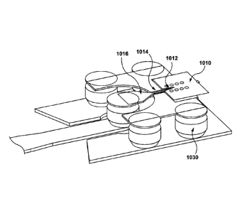
10;
and
[0017] Figure 13 illustrates a flow chart of a method in accordance with
one or
more embodiments.
DETAILED DESCRIPTION
[0018] The present disclosure is directed in general to communications
systems
and methods for operating the same. More specifically, aspects of the
disclosure are
directed to transitions between integrated circuits (ICs) and printed circuit
boards
(PCBs).
2
CA 02867246 2014-10-08
[0019] Embodiments are directed to a transition structure for interfacing
an
integrated circuit chip and a substrate, comprising: a vertical transmission
section
configured to bridge two layers of a package between two ground planes, a
transmission line formed between the ground planes and connected to a center
of the
vertical transmission section, a second vertical transmission section coupled
to the
transmission line and a layer of the package, a plurality of solder
connections coupled
to the layer of the package, and a microstrip coupled to at least one of the
solder
connections.
[0020] Embodiments are directed to a transition structure for interfacing
an
integrated circuit chip and a substrate, comprising: a co-planar waveguide
(CPW)
structure formed based on ground-signal-ground (GSG) pads on the integrated
circuit
chip, a grounded co-planar waveguide (CPWG) structure coupled to the GSG pads,
and a microstrip coupled to the CPWG structure.
[0021] Embodiments are directed to a transition structure for interfacing
an
integrated circuit chip and a substrate, comprising: a microstrip coupled to a
grounded
co-planar waveguide (CPWG) structure, a co-planar waveguide (CPW) structure
coupled to the CPWG structure, wherein the CPWG structure transitions to the
CPW
structure based on a taper in a signal line and a triangular notch in a ground
plane, and
balls of a package coupled to the CPW structure.
[0022] Various illustrative embodiments of the present disclosure will now
be
described in detail with reference to the accompanying figures. While various
details
are set forth in the following description, it will be appreciated that the
present
disclosure may be practiced without these specific details, and that numerous
implementation-specific decisions may be made to the disclosure described
herein to
achieve specific goals, such as compliance with process technology or design-
related
constraints, which will vary from one implementation to another. While such a
development effort might be complex and time-consuming, it would nevertheless
be a
routine undertaking for those of skill in the art having the benefit of this
disclosure.
For example, selected aspects are shown in block diagram and flowchart form,
rather
than in detail, in order to avoid limiting or obscuring the present
disclosure. In
addition, some portions of the detailed descriptions provided herein are
presented in
terms of algorithms or operations on data within a computer memory. Such
3
CA 02867246 2014-10-08
descriptions and representations are used by those skilled in the art to
describe and
convey the substance of their work to others skilled in the art.
[0023] As used herein, the terms "component," -system" and the like are
intended
to refer to a computer-related entity, either hardware, software, a
combination of
hardware and software, or software in execution. For example, a component may
be,
but is not limited to being, a processor, a process running on a processor, an
object, an
executable instruction sequence, a thread of execution, a program, or a
computer. In
an example, a component may be, but is not limited to being, circuitry, a
process
running on circuitry, an object, an executable instruction sequence, a thread
of
execution, a program, or a computing device. By way of illustration, both an
application running on a computer and the computer itself can be a component.
One
or more components may reside within a process or thread of execution and a
component may be localized on one computer or distributed between two or more
computers.
[0024] As likewise used herein, the term "node" broadly refers to a
connection
point, such as a redistribution point or a communication endpoint, of a
communication
environment, such as a network. Accordingly, such nodes refer to an active
electronic
device capable of sending, receiving, or forwarding information over a
communications channel. Examples of such nodes include data circuit-
terminating
equipment (DCE), such as a modem, hub, bridge or switch, and data terminal
equipment (DTE), such as a handset, a printer or a host computer (e.g., a
router,
workstation or server). Examples of local area network (LAN) or wide area
network
(WAN) nodes include computers, packet switches, cable modems, Data Subscriber
Line (DSL) modems, and wireless LAN (WLAN) access points. Examples of Internet
or Intranet nodes include host computers identified by an Internet Protocol
(IP)
address, bridges and WLAN access points. Likewise, examples of nodes in
cellular
communication include base stations, relays, base station controllers, radio
network
controllers, home location registers (HLR), visited location registers (VLR),
Gateway
GPRS Support Nodes (GGSN), Serving GPRS Support Nodes (SGSN), Serving
Gateways (S-GW), and Packet Data Network Gateways (PDN-GW).
4
CA 02867246 2014-10-08
[0025] Other examples of nodes include client nodes, server nodes, peer
nodes
and access nodes. As used herein, a client node may refer to wireless devices
such as
mobile telephones, smart phones, personal digital assistants (PDAs), handheld
devices, portable computers, tablet computers, and similar devices or other
user
equipment (UE) that has telecommunications capabilities. Such client nodes may
likewise refer to a mobile, wireless device, or alternatively, to devices that
have
similar capabilities that are not generally transportable, such as desktop
computers,
set-top boxes, or sensors. A network node, as used herein, generally includes
all
nodes with the exception of client nodes, server nodes and access nodes.
Likewise, a
server node, as used herein, refers to an information processing device (e.g.,
a host
computer), or series of information processing devices, that perform
information
processing requests submitted by other nodes. As likewise used herein, a peer
node
may sometimes serve as client node, and at other times, a server node. In a
peer-to-
peer or overlay network, a node that actively routes data for other networked
devices
as well as itself may be referred to as a supernode.
[0026] An access node, as used herein, refers to a node that provides a
client node
access to a communication environment. Examples of access nodes include
cellular
network base stations and wireless broadband (e.g., WiFi, WiMAX, etc.) access
points, which provide corresponding cell and WLAN coverage areas. As used
herein,
a macrocell is used to generally describe a traditional cellular network cell
coverage
area. Such macrocells are typically found in rural areas, along highways, or
in less
populated areas. As likewise used herein, a microcell refers to a cellular
network cell
with a smaller coverage area than that of a macrocell. Such micro cells are
typically
used in a densely populated urban area. Likewise, as used herein, a picocell
refers to
a cellular network coverage area that is less than that of a microcell. An
example of
the coverage area of a picocell may be a large office, a shopping mall, or a
train
station. A femtocell, as used herein, currently refers to the smallest
commonly
accepted area of cellular network coverage. As an example, the coverage area
of a
femtocell is sufficient for homes or small offices.
[0027] In general, a coverage area of less than two kilometers typically
corresponds to a microcell, 200 meters or less for a picocell, and on the
order of 10
CA 02867246 2014-10-08
meters for a femtocell. The actual dimensions of the cell may depend on the
radio
frequency of operation, the radio propagation conditions and the density of
communications traffic. As likewise used herein, a client node communicating
with
an access node associated with a macrocell is referred to as a "macrocell
client."
Likewise, a client node communicating with an access node associated with a
microcell, picocell, or femtocell is respectively referred to as a -microcell
client,"
"picocell client," or "femtocell client."
[0028] The term "article of manufacture" (or alternatively, -computer
program
product") as used herein is intended to encompass a computer program
accessible
from any computer-readable device or media, e.g., machine readable media. For
example, computer readable media can include but are not limited to magnetic
storage
devices (e.g., hard disk, floppy disk, magnetic strips, etc.), optical disks
such as a
compact disk (CD) or digital versatile disk (DVD), smart cards, and flash
memory
devices (e.g., card, stick, etc.). In an example, the machine readable media
is in a
tangible form capable of being detected by a machine, data being generated
therefrom
and such data being manipulated and transformed by a machine.
[0029] The word "exemplary" is used herein to mean serving as an example,
instance, or illustration. Any aspect or design described herein as
"exemplary" is not
necessarily to be construed as preferred or advantageous over other aspects or
designs. Those of skill in the art will recognize many modifications may be
made to
this configuration without departing from the scope, spirit or intent of the
claimed
subject matter. Furthermore, the disclosed subject matter may be implemented
as a
system, method, apparatus, or article of manufacture using standard
programming and
engineering techniques to produce software, firmware, hardware, or any
combination
thereof to control a computer or processor-based device to implement aspects
detailed
herein.
[0030] Figure 1 illustrates an example of a system 100 suitable for
implementing
one or more embodiments disclosed herein. In various embodiments, the system
100
comprises a processor 110, which may be referred to as a central processor
unit
(CPU) or digital signal processor (DSP), network connectivity interfaces 120,
random
access memory (RAM) 130, read only memory (ROM) 140, secondary storage 150,
6
CA 02867246 2014-10-08
and input/output (I/O) devices 160. In some embodiments, some of these
components
may not be present or may be combined in various combinations with one another
or
with other components not shown. These components may be located in a single
physical entity or in more than one physical entity. Any actions described
herein as
being taken by the processor 110 might be taken by the processor 110 alone or
by the
processor 110 in conjunction with one or more components shown or not shown in
Figure 1.
[0031] The processor 110 executes instructions, codes, computer programs,
or
scripts that it might access from the network connectivity interfaces 120, RAM
130,
or ROM 140. While only one processor 110 is shown, multiple processors may be
present. Thus, while instructions may be discussed as being executed by a
processor
110, the instructions may be executed simultaneously, serially, or otherwise
by one or
multiple processors 110 implemented as one or more CPU chips.
[0032] In various embodiments, the network connectivity interfaces 120 may
take
the form of modems, modem banks, Ethernet devices, universal serial bus (USB)
interface devices, serial interfaces, token ring devices, fiber distributed
data interface
(FDDI) devices, wireless local area network (WLAN) devices (including radio,
optical or infra-red signals), radio transceiver devices such as code division
multiple
access (CDMA) devices, global system for mobile communications (GSM) radio
transceiver devices, long term evolution (LTE) radio transceiver devices,
worldwide
interoperability for microwave access (WiMAX) devices, and/or other well-known
interfaces for connecting to networks, including Personal Area Networks (PANs)
such
as Bluetooth. These network connectivity interfaces 120 may enable the
processor
110 to communicate with the Internet or one or more telecommunications
networks or
other networks from which the processor 110 might receive information or to
which
the processor 110 might output information.
[0033] The network connectivity interfaces 120 may also be capable of
transmitting or receiving data wirelessly in the form of electromagnetic
waves, such
as radio frequency signals or microwave frequency signals. Information
transmitted
or received by the network connectivity interfaces 120 may include data that
has been
processed by the processor 110 or instructions that are to be executed by
processor
7
CA 02867246 2014-10-08
110. The data may be ordered according to different sequences as may be
desirable
for either processing or generating the data or transmitting or receiving the
data.
[0034] In various embodiments, the RAM 130 may be used to store volatile
data
and instructions that are executed by the processor 110. The ROM 140 shown in
Figure 1 may likewise be used to store instructions and data that is read
during
execution of the instructions. The secondary storage 150 is typically
comprised of
one or more disk drives, solid state drives, or tape drives and may be used
for non-
volatile storage of data or as an overflow data storage device if RAM 130 is
not large
enough to hold all working data. Secondary storage 150 may likewise be used to
store programs that are loaded into RAM 130 when such programs are selected
for
execution. The I/O devices 160 may include liquid crystal displays (LCDs),
Light
Emitting Diode (LED) displays, Organic Light Emitting Diode (OLED) displays,
projectors, televisions, touch screen displays, keyboards, keypads, switches,
dials,
mice, track balls, track pads, voice recognizers, card readers, paper tape
readers,
printers, video monitors, or other well-known input/output devices.
[0035] Figure 2 shows a wireless-enabled communications environment
including
an embodiment of a client node as implemented in an embodiment of the
disclosure.
Though illustrated as a mobile phone, the client node 202 may take various
forms
including a wireless handset, a pager, a smart phone, or a personal digital
assistant
(PDA). In various embodiments, the client node 202 may also comprise a
portable
computer, a tablet computer, a laptop computer, or any computing device
operable to
perform data communication operations. Many suitable devices combine some or
all
of these functions. In some embodiments, the client node 202 is not a general
purpose
computing device like a portable, laptop, or tablet computer, but rather is a
special-
purpose communications device such as a telecommunications device installed in
a
vehicle. The client node 202 may likewise be a device, include a device, or be
included in a device that has similar capabilities but that is not
transportable, such as a
desktop computer, a set-top box, or a network node. In these and other
embodiments,
the client node 202 may support specialized activities such as gaming,
inventory
control, job control, task management functions, and so forth.
8
CA 02867246 2014-10-08
[0036] In various embodiments, the client node 202 includes a display 204.
In
these and other embodiments, the client node 202 may likewise include a touch-
sensitive surface, a keyboard or other input keys 206 generally used for input
by a
user. The input keys 206 may likewise be a full or reduced alphanumeric
keyboard
such as QWERTY, DVORAK, AZERTY, and sequential keyboard types, or a
traditional numeric keypad with alphabet letters associated with a telephone
keypad.
The input keys 206 may likewise include a trackwheel, an exit or escape key, a
trackball, a track pad and other navigational or functional keys, which may be
moved
to different positions, e.g., inwardly depressed, to provide further input
function. The
client node 202 may likewise present options for the user to select, controls
for the
user to actuate, and cursors or other indicators for the user to direct.
[0037] The client node 202 may further accept data entry from the user,
including
numbers to dial or various parameter values for configuring the operation of
the client
node 202. The client node 202 may further execute one or more software or
firmware
applications in response to user commands. These applications may configure
the
client node 202 to perform various customized functions in response to user
interaction. Additionally, the client node 202 may be programmed or configured
over-the-air (OTA), for example from a wireless network access node 'A' 210
through 'n' 216 (e.g., a base station), a server node 224 (e.g., a host
computer), or a
peer client node 202.
[0038] Among the various applications executable by the client node 202 are
a
web browser, which enables the display 204 to display a web page. The web page
may be obtained from a server node 224 through a wireless connection with a
wireless
network 220. As used herein, a wireless network 220 broadly refers to any
network
using at least one wireless connection between two of its nodes. The various
applications may likewise be obtained from a peer client node 202 or other
system
over a connection to the wireless network 220 or any other wirelessly-enabled
communication network or system.
[0039] In various embodiments, the wireless network 220 comprises a
plurality of
wireless sub-networks (e.g., cells with corresponding coverage areas) 'A' 212
through
'n' 218. As used herein, the wireless sub-networks `A. 212 through 'n' 218 may
9
CA 02867246 2014-10-08
variously comprise a mobile wireless access network or a fixed wireless access
network. In these and other embodiments, the client node 202 transmits and
receives
communication signals, which are respectively communicated to and from the
wireless network nodes 'A' 210 through 'n' 216 by wireless network antennas
'A'
208 through 'n' 214 (e.g., cell towers). In turn, the communication signals
are used
by the wireless network access nodes 'A' 210 through 'n' 216 to establish a
wireless
communication session with the client node 202. As used herein, the network
access
nodes 'A' 210 through 'n' 216 broadly refer to any access node of a wireless
network.
As shown in Figure 2, the wireless network access nodes 'A' 210 through 'n'
216 are
respectively coupled to wireless sub-networks 'A' 212 through 'n' 218, which
are in
turn connected to the wireless network 220.
[0040] In various embodiments, the wireless network 220 is coupled to a
core
network 222, e.g., a global computer network such as the Internet. Via the
wireless
network 220 and the core network 222, the client node 202 has access to
information
on various hosts, such as the server node 224. In these and other embodiments,
the
server node 224 may provide content that may be shown on the display 204 or
used
by the client node processor 110 for its operations. Alternatively, the client
node 202
may access the wireless network 220 through a peer client node 202 acting as
an
intermediary, in a relay type or hop type of connection. As another
alternative, the
client node 202 may be tethered and obtain its data from a linked device that
is
connected to the wireless sub-network 212. Skilled practitioners of the art
will
recognize that many such embodiments are possible and the foregoing is not
intended
to limit the spirit, scope, or intention of the disclosure.
[0041] Figure 3 depicts a block diagram of an exemplary client node as
implemented with a digital signal processor (DSP) in accordance with an
embodiment
of the disclosure. While various components of a client node 202 are depicted,
various embodiments of the client node 202 may include a subset of the listed
components or additional components not listed. As shown in Figure 3, the
client
node 202 includes a DSP 302 and a memory 304. As shown, the client node 202
may
further include an antenna and front end unit 306, a radio frequency (RF)
transceiver
308, an analog baseband processing unit 310, a microphone 312, an earpiece
speaker
CA 02867246 2014-10-08
314, a headset port 316, a bus 318, such as a system bus or an input/output
(I/O)
interface bus, a removable memory card 320, a universal serial bus (USB) port
322, a
short range wireless communication sub-system 324, an alert 326, a keypad 328,
a
liquid crystal display (LCD) 330, which may include a touch sensitive surface,
an
LCD controller 332, a charge-coupled device (CCD) camera 334, a camera
controller
336, and a global positioning system (GPS) sensor 338, and a power management
module 340 operably coupled to a power storage unit, such as a battery 342. In
various embodiments, the client node 202 may include another kind of display
that
does not provide a touch sensitive screen. In one embodiment, the DSP 302
communicates directly with the memory 304 without passing through the
input/output
interface ("Bus") 318.
[0042] In various embodiments, the DSP 302 or some other form of controller
or
central processing unit (CPU) operates to control the various components of
the client
node 202 in accordance with embedded software or firmware stored in memory 304
or stored in memory contained within the DSP 302 itself. In addition to the
embedded
software or firmware, the DSP 302 may execute other applications stored in the
memory 304 or made available via information media such as portable data
storage
media like the removable memory card 320 or via wired or wireless network
communications. The application software may comprise a compiled set of
machine-
readable instructions that configure the DSP 302 to provide the desired
functionality,
or the application software may be high-level software instructions to be
processed by
an interpreter or compiler to indirectly configure the DSP 302.
[0043] The antenna and front end unit 306 may be provided to convert
between
wireless signals and electrical signals, enabling the client node 202 to send
and
receive information from a cellular network or some other available wireless
communications network or from a peer client node 202. In an embodiment, the
antenna and front end unit 106 may include multiple antennas to support beam
forming and/or multiple input multiple output (MIMO) operations. As is known
to
those skilled in the art, MIMO operations may provide spatial diversity, which
can be
used to overcome difficult channel conditions or to increase channel
throughput.
Likewise, the antenna and front-end unit 306 may include circuitry, for
example,
11
CA 02867246 2014-10-08
antenna tuning or impedance matching components, RF power amplifiers, or low
noise amplifiers.
[0044] In various embodiments, the RF transceiver 308 provides frequency
shifting, converting received RF signals to baseband and converting baseband
transmit signals to RF. In some descriptions a radio transceiver or RF
transceiver
may be understood to include other signal processing functionality such as
modulation/demodulation, coding/decoding, interleaving/deinterleaving,
spreading/despreading, inverse fast Fourier transforming (IFFT)/fast Fourier
transforming (FFT), cyclic prefix appending/removal, and other signal
processing
functions. For the purposes of clarity, the description here separates the
description of
this signal processing from the RF and/or radio stage and conceptually
allocates that
signal processing to the analog baseband processing unit 310 or the DSP 302 or
other
central processing unit. In some embodiments, the RF Transceiver 108, portions
of
the Antenna and Front End 306, and the analogbase band processing unit 310 may
be
combined in one or more processing units and/or application specific
integrated
circuits (ASICs).
[0045] Note that in this diagram the radio access technology (RAT) RAT1 and
RAT2 transceivers 354, 358, the IXRF 356, the IRSL 352 and Multi-RAT subsystem
350 are operably coupled to the RF transceiver 308 and analog baseband
processing
unit 310 and then also coupled to the antenna and front end 306 via the RF
transceiver
308. As there may be multiple RAT transceivers, there will typically be
multiple
antennas or front ends 306 or RF transceivers 308, one for each RAT or band of
operation.
[0046] The analog baseband processing unit 310 may provide various analog
processing of inputs and outputs for the RF transceivers 308 and the speech
interfaces
(312, 314, 316). For example, the analog baseband processing unit 310 receives
inputs from the microphone 312 and the headset 316 and provides outputs to the
earpiece 314 and the headset 316. To that end, the analog baseband processing
unit
310 may have ports for connecting to the built-in microphone 312 and the
earpiece
speaker 314 that enable the client node 202 to be used as a cell phone. The
analog
baseband processing unit 310 may further include a port for connecting to a
headset or
12
CA 02867246 2014-10-08
other hands-free microphone and speaker configuration. The analog baseband
processing unit 310 may provide digital-to-analog conversion in one signal
direction
and analog-to-digital conversion in the opposing signal direction. In various
embodiments, at least some of the functionality of the analog baseband
processing
unit 310 may be provided by digital processing components, for example by the
DSP
302 or by other central processing units.
[0047] The DSP 302 may perform modulation/demodulation, coding/decoding,
interleaving/deinterleaving, spreading/despreading, inverse fast Fourier
transforming
(IFFT)/fast Fourier transforming (FFT), cyclic prefix appending/removal, and
other
signal processing functions associated with wireless communications. In an
embodiment, for example in a code division multiple access (CDMA) technology
application, for a transmitter function the DSP 302 may perform modulation,
coding,
interleaving, and spreading, and for a receiver function the DSP 302 may
perform
despreading, deinterleaving, decoding, and demodulation. In another
embodiment,
for example in an orthogonal frequency division multiplex access (OFDMA)
technology application, for the transmitter function the DSP 302 may perform
modulation, coding, interleaving, inverse fast Fourier transforming, and
cyclic prefix
appending, and for a receiver function the DSP 302 may perform cyclic prefix
removal, fast Fourier transforming, deinterleaving, decoding, and
demodulation. In
other wireless technology applications, yet other signal processing functions
and
combinations of signal processing functions may be performed by the DSP 302.
[0048] The DSP 302 may communicate with a wireless network via the analog
baseband processing unit 310. In some embodiments, the communication may
provide global computer network (e.g., Internet) connectivity, enabling a user
to gain
access to content on the global computer network and to send and receive e-
mail or
text messages. The input/output interface 318 interconnects the DSP 302 and
various
memories and interfaces. The memory 304 and the removable memory card 320 may
provide software and data to configure the operation of the DSP 302. Among the
interfaces may be the USB interface 322 and the short range wireless
communication
sub-system 324. The USB interface 322 may be used to charge the client node
202
and may also enable the client node 202 to function as a peripheral device to
13
CA 02867246 2014-10-08
exchange information with a personal computer or other computer system. The
short
range wireless communication sub-system 324 may include an infrared port, a
Bluetooth interface, an IEEE 802.11 compliant wireless interface, or any other
short
range wireless communication sub-system, which may enable the client node 202
to
communicate wirelessly with other nearby client nodes and access nodes. The
short-
range wireless communication Sub-system 324 may also include suitable RF
Transceiver, Antenna and Front End subsystems.
[0049] The input/output interface ("Bus") 318 may further connect the DSP
302
to the alert 326 that, when triggered, causes the client node 202 to provide a
notice to
the user, for example, by ringing, playing a melody, or vibrating. The alert
326 may
serve as a mechanism for alerting the user to any of various events such as an
incoming call, a new text message, and an appointment reminder by silently
vibrating,
or by playing a specific pre-assigned melody for a particular caller.
[0050] The keypad 328 couples to the DSP 302 via the I/O interface ("Bus")
318
to provide one mechanism for the user to make selections, enter information,
and
otherwise provide input to the client node 202. The keyboard 328 may be a full
or
reduced alphanumeric keyboard such as QWERTY, DVORAK, AZERTY and
sequential types, or a traditional numeric keypad with alphabet letters
associated with
a telephone keypad. The input keys may likewise include a trackwheel, track
pad, an
exit or escape key, a trackball, and other navigational or functional keys,
which may
be inwardly depressed to provide further input function. Another input
mechanism
may be the LCD 330, which may include touch screen capability and also display
text
and/or graphics to the user. The LCD controller 332 couples the DSP 302 to the
LCD
330.
[0051] The CCD camera 334, if equipped, enables the client node 202 to make
digital pictures. The DSP 302 communicates with the CCD camera 334 via the
camera controller 336. In another embodiment, a camera operating according to
a
technology other than Charge Coupled Device cameras may be employed. The GPS
sensor 338 is coupled to the DSP 302 to decode global positioning system
signals or
other navigational signals, thereby enabling the client node 202 to determine
its
position. The GPS sensor 338 may be coupled to an antenna and front end (not
14
CA 02867246 2014-10-08
shown) suitable for its band of operation. Various other peripherals may also
be
included to provide additional functions, such as radio and television
reception.
[0052] In various embodiments, the client node (e.g., 202) comprises a
first Radio
Access Technology (RAT) transceiver 354 and a second RAT transceiver 358. As
shown in Figure 3, and described in greater detail herein, the RAT
transceivers '1'
354 and '2' 358 are in turn coupled to a multi-RAT communications subsystem
350
by an Inter-RAT Supervisory Layer Module 352. In turn, the multi- RAT
communications subsystem 350 is operably coupled to the Bus 318. Optionally,
the
respective radio protocol layers of the first Radio Access Technology (RAT)
transceiver 354 and the second RAT transceiver 358 are operably coupled to one
another through an Inter-RAT eXchange Function (IRXF) Module 356.
[0053] In various embodiments, the network node (e.g. 224) acting as a
server
comprises a first communication link corresponding to data to/from the first
RAT and
a second communication link corresponding to data to/from the second RAT.
[0054] Embodiments of the disclosure may be associated with communication
at
radio frequency (RF). For example, aspects of the disclosure may be used in
connection with millimeter wave (mmWave) radio. In some embodiments, a 60 GHz
spectrum may include one or more channels, bands or ranges. For example, a
first
range may be from 57.2 GHz ¨ 59.4 GHz, a second range may be from 59.4 GHz to
61.5 GHz, a third range may be from 61.5 GHz to 63.7 GHz, and a fourth range
may
be from 63.7 GHz to 65.8 GHz.
[0055] As described above, embodiments of the disclosure may be used to
facilitate a transition from an IC package to a PCB. One or more package
configurations may be used, such as a low temperature co-fired ceramic (LTCC)
package, a flip-chip package, and a wafer level fan-out (WLFO) package.
[0056] Referring to Figure 4, a basic package configuration 400 in
accordance
with one or more embodiments is shown. The package configuration 400 may be
used in connection with an LTCC package, or any package or package material
with a
similar orientation. Package configuration 400 can connect an array of mmWave
antennas to other circuitry, e.g., on the PCB, in a mobile electronic device.
CA 02867246 2014-10-08
[0057] The package configuration 400 includes an IC 402 coupled to an IC
package 404. The IC 402 may be inverted inside the package 404 relative to
conventional mounting or coupling techniques. Included in the package 404 may
be
one or more connections 406 to facilitate connecting the IC 402 to a PCB 408.
The
connection may occur using a solder connection, e.g., ball grid array (BGA)
solder
balls 410.
[0058] Referring now to Figure 5, a transition structure 500 for
facilitating the
connection 406 from the IC 402 to the PCB 408 is shown. Ground-signal-ground
(GSG) pads on the IC 402 may create a co-planar waveguide (CPW) structure.
Referring to Figure 6, this CPW structure may be continued above in a first
layer of
the package 404 with vias 602 going to the next or second layer. Connections
between the IC 402 and the package 404 may be facilitated by one or more
solder
connections, e.g., solder balls 604. Underfill 612 may be used between the IC
and the
package as shown in Figure 6. Similarly, underfill 512 may be used between the
package and PCB as reflected in Figure 5.
[0059] As described below, the structure 500 may make use of stripline. As
used
herein, stripline refers to a transverse electromagnetic (TEM) transmission
line
medium that uses a flat strip of conductor/metal sandwiched between parallel
ground
planes. The stripline may be supported by a dielectric.
[0060] Starting from the second layer above the IC 402, a chip to stripline
transition or quasi-coax line/section 506, as would be known to one of skill
in the art,
may bridge two layers of the package 404 between two ground planes 608, where
the
ground planes 608 may be different ground planes. A stripline 510 may be
formed
between the ground planes 608 and may be connected to a center of the coax
section
506.
[0061] In some embodiments the stripline 510 may carry signal in an area
directly
above where the IC 402 is mounted to the package 404 to an area on the
perimeter of
the package 404 where solder balls for the package (e.g., solder balls 410)
may be
placed.
16
CA 02867246 2014-10-08
[0062] Referring to Figures 5 and 7, the signal may be carried by the
stripline 510
to a stripline-to-PCB or quasi-coax transition/section 514 (which may be
similar to, or
different from, the transition 506). The signal may be conveyed by the
transition/section 514 through one or more layers of the package 404 to the
bottom of
the package 404.
[0063] Referring to Figures 7 and 8, the final or bottom layer of the
package 404
may translate the signal and ground into, e.g., four solder balls 720, which
may match
pads designed in the PCB 408. The solder balls 720 may correspond to the
solder
balls 410 of Figure 4.
[0064] The arrangement shown in Figures 7 and 8 may be similar to the GSG
arrangement described above in connection with the pads of the chip 402, but
an
additional, back ground signal may be included to reduce the radiation of the
GSG
balls from the package 404 to the PCB 408. In some instances, the solder balls
720
may have a pitch of 0.5 millimeters and the height of substrate may be enough
that it
may otherwise be difficult to avoid radiation between the package 404 and the
PCB
408 without the inclusion of the additional ground signal.
[0065] The transition from the package 404 to the PCB 408 may take the
three
ground connections (e.g. solder balls) and one signal connection (e.g., ball)
and
transition to a ground coupled co-planar waveguide (CPWG). In such a design, a
ground via 822 may be placed behind the transition in the PCB 408 to provide a
direct
current (DC) path to ground. The CPWG on the PCB 408 may then transition 526
through a taper to a microstrip line 830. In some embodiments, the ground via
822
might not be included. In some embodiments, there may be two ground balls on
either side of a signal ball, and a back ground ball might not be used.
[0066] As an illustrative example, in some embodiments solder ball pitch
(e.g.,
solder balls 410 or 720) may be 500 micrometers, a substrate height of the PCB
408
may be 50 micrometers, and as shown in Figure 8 a 'T" pattern may be used in
connection with the solder balls 720 with a signal solder ball in the middle
surrounded
by three ground solder balls. In yet another illustrative embodiment, the
solder ball
pitch may be 400 micrometers, the substrate height of the PCB may be 100
17
CA 02867246 2014-10-08
micrometers, and the transition may use a full BGA array (as opposed to the
'T'
pattern).
[0067] Referring to Figures 9A-9B (collectively referred to as Figure 9), a
transition implemented in connection with a flip-chip is shown. Specifically,
Figure
9A reflects a top view of the transition and Figure 9B reflects a complete
model of the
transition.
[0068] As shown in Figure 9, much like the embodiments described above in
connection with LTCC and similar packaging, the flip-chip design may use pads
944
(e.g., GSG pads) on an IC 902 to create an effective CPW structure. This
structure
may be continued through balls on bare die.
[0069] The GSG balls/pads may connect to a CPWG structure 906 on PCB 908.
The CPWG structure 906 may include one or more extra ground balls
corresponding
to ground points in the design of the IC 902. A ground ring may be designed to
accommodate ground domains in connection with the IC 902 and the PCB 908,
which
may be motivated at least in part based on the pitch associated with the IC
902. The
ground ring may be vialess.
[0070] A tapered transition 914 may be used between the CPWG structure 906
and a microstrip 930. The rest of the structures of Figure 9 surrounding the
CPWG
section 906 are specific to the IC 902 and are included for simulating their
coupling
effect.
[0071] Flip-chip may represent an attractive package option due to a
simplified
number of layers for a mmWave transition. But, flip-chip may impose difficulty
in
connection with low-cost PCB fabrication. For example, a flip-chip may have a
pad
pitch on the order of, e.g., 160 micrometers, whereas standard BOA assembly
capabilities for high volume production may require a pitch of at least 350
micrometers. In order to remedy such a situation, a chip-scale package (CSP)
with re-
distribution layers called wafer level fan-out (WLF0) may be used in some
embodiments. The WLFO package may provide for an increase in pitch without
adding much complexity (e.g., layers) and cost to the IC.
18
CA 02867246 2014-10-08
[0072] Referring to Figure 10, a transition implemented in connection with
WLFO is shown. The WLFO transition may include GSG pads on the IC to create an
(effective) CPW structure. Vias in the WLFO structure may connect this CPW
structure to the chip-side of the transition (Figure 11) where a small CPW
structure
transitions into a microstrip 1010. From the point of view of the finished PCB
this
microstrip 1010 may be upside-down. For example, the ground for the microstrip
may be in the first WLFO layer (WLP layer 1 in Figure 10, layer L1 in Figure
11) and
signal may be in the second layer (WLP layer 2 in Figure 10, layer L2 in
Figure 11).
The ground of the PCB may be much further away and might not appreciably
impact
the microstrip.
[0073] Referring to Figures 10 and 12A, the microstrip 1010 may transition
1012
to a CPWG. A row of vias 1228 may be present on either side to connect the
microstrip ground to the CPWG ground side.
[0074] Referring to Figure 10, the CPWG may then transition to a pure CPW
(e.g., a co-planar waveguide with no ground) 1014. This may be done with a
taper in
the signal line and a triangular notch in the ground plane.
[0075] The CPW may then transition to the balls (e.g., BGA balls) of the
package
1016.
[0076] Whereas Figure 12A depicts an exemplary view of the WLFO package
from the bottom, Figure 12B depicts an exemplary view of the PCB section from
the
top. As shown in Figure 12B, a PCB via 1252 may be present to provide a direct
current (DC) path to ground and one or more balls 1030 may facilitate coupling
the
WLFO package and the PCB. In some embodiments, the balls 1030 may have a
"collapsed height" of 180 microns.
[0077] The transition from the package WLFO package in Figure 12A to the
PCB
in Figure 12B may take the four ground balls 1030a and one signal ball 1030b
and
transition to a ground coupled co-planar waveguide (CPWG) 1256. In such a
design,
a ground via 1252 may be placed behind the transition in the PCB to provide a
direct
current (DC) path to ground. The CPWG 1256 on the PCB may then transition
through a taper to a microstrip line 1258.
19
CA 02867246 2014-10-08
[0078] Referring to Figure 13, a flow chart of an exemplary method 1300 is
shown. The method 1300 may execute in connection with one or more components,
devices, or systems, such as those described herein. The method 1300 may be
used to
design and implement an interface transition between an IC and a PCB in
connection
with one or more package types. The design may facilitate use or operation at
mmWave frequencies.
[0079] In block 1302, a package type or configuration for an IC may be
selected.
The selection of block 1302 may be based on one or more requirements. For
example, cost of production, functionality needed, and other factors may be
taken into
consideration when selecting the package.
[0080] In block 1304, a transition structure may be selected. The selection
of
block 1304 may be based on the selection of block 1302. The selected
transition
structure may include one or more components, such as GSG pads, one or more
quasi-
coax structures, striplines, microstrip, CPW, CPWG, solder balls, etc.
[0081] In block 1306, the IC may be coupled to, or formed within, the
package.
[0082] In block 1308, the package may be coupled to the PCB.
[0083] The method 1300 is illustrative. In some embodiments, one or more of
the
blocks or operations (or a portion thereof) may be optional. In some
embodiments,
additional blocks or operations may be included. In some embodiments, the
blocks
may execute in an order or sequence different from what is shown in Figure 13.
[0084] The present description references ground, e.g., ground plane(s),
ground connections, etc. It will be understood that ground can be Earth or
zero
potential. In other examples, ground is not necessarily Earth potential, and a
-ground
line" or "ground plane" need not be electrically connected to the Earth.
Rather,
ground basically connotes a node that is maintained at a reference voltage
that is
substantially constant with respect to other voltages in the structures and
circuitry
described herein.
[0085] Embodiments are directed to a transition structure for interfacing
an
integrated circuit chip (402) and a substrate (408), comprising: a vertical
transmission
CA 02867246 2014-10-08
section (506) configured to bridge two layers of a package (404) between two
ground
planes; a transmission line (510) formed between the ground planes and
connected to
a center of the vertical transmission section (506); a second vertical
transmission
section (514) coupled to the transmission line (510) and a layer of the
package (404);
a plurality of solder connections (720) coupled to the layer of the package
(404); and
a microstrip (830) coupled to at least one of the solder connections (720).
The
microstrip (830) may be coupled to the at least one of the solder connections
(720)
through a grounded co-planar waveguide structure (526). The transmission line
(510)
may comprise a stripline (510). At least one of the vertical transmission
section (510)
and the second vertical transmission section (514) may comprise a quasi-coax
section
(510, 514). The transmission line (510) may be configured to convey a
millimeter
wave signal associated with the integrated circuit (402). The at least one
solder
connection (720) may be associated with the signal, and the remainder of the
solder
connections (720) may be associated with a ground. The transition structure
may
comprise a via (822) configured to provide a direct current path to ground.
The
package (404) may be a low temperature co-fired ceramic package (404).
[0086] Embodiments are directed to a transition structure for interfacing
an
integrated circuit chip (902) and a substrate (908), comprising: a co-planar
waveguide
structure formed based on ground-signal-ground pads (944) on the integrated
circuit
chip (902); a grounded co-planar waveguide structure coupled to the ground-
signal-
ground pads (944); and a microstrip (930) coupled to the grounded co-planar
waveguide structure. The transition structure may be associated with a flip-
chip
package. The transition structure may be configured to operate in accordance
with a
60 GHz spectrum.
[0087] Embodiments are directed to a transition structure for interfacing
an
integrated circuit chip and a substrate, comprising: a microstrip (1010)
coupled to a
grounded co-planar waveguide structure (1012); a co-planar waveguide structure
(1014) coupled to the grounded co-planar waveguide structure (1012), wherein
the
grounded co-planar waveguide structure (1012) transitions to the co-planar
waveguide
structure (1014) based on a taper in a signal line and a triangular notch in a
ground
plane; and balls (1030) of a package coupled to the co-planar waveguide
structure
21
CA 02867246 2014-10-08
(1014). A ground of the microstrip (1010) may be located in a first layer of
the
transition structure and the signal line may be associated with the microstrip
(1010)
and a second layer of the transition structure. The package may be a wafer
level fan-
out package. The transition structure may be configured to operate in
accordance
with a 60 GHz spectrum.
[0088] As described herein, in some embodiments various functions or acts
may
take place at a given location and/or in connection with the operation of one
or more
apparatuses, systems, or devices. For example, in some embodiments, a portion
of a
given function or act may be performed at a first device or location, and the
remainder
of the function or act may be performed at one or more additional devices or
locations.
[0089] Embodiments of the disclosure may be implemented using one or more
technologies. In some embodiments, an apparatus or system may include one or
more
processors, and memory storing instructions that, when executed by the one or
more
processors, cause the apparatus or system to perform one or more
methodological acts
as described herein. Various mechanical components known to those of skill in
the
art may be used in some embodiments.
[0090] Embodiments of the disclosure may be implemented as one or more
apparatuses, systems, and/or methods. In some embodiments, instructions may be
stored on one or more computer-readable media, such as a transitory and/or non-
transitory computer-readable medium. The instructions, when executed, may
cause
an entity (e.g., an apparatus or system) to perform one or more methodological
acts as
described herein. In some embodiments, the functionality described herein may
be
implemented in hardware, software, firmware, or any combination thereof.
[0091] The particular embodiments disclosed above are illustrative only and
should not be taken as limitations upon the present disclosure, as the
disclosure may
be modified and practiced in different but equivalent manners apparent to
those
skilled in the art having the benefit of the teachings herein. Accordingly,
the
foregoing description is not intended to limit the disclosure to the
particular form set
forth, but on the contrary, is intended to cover such alternatives,
modifications and
22
CA 02867246 2014-10-08
equivalents as may be included within the spirit and scope of the disclosure
as defined
by the appended claims so that those skilled in the art should understand that
they can
make various changes, substitutions and alterations without departing from the
spirit
and scope of the disclosure in its broadest form.
23