Note: Descriptions are shown in the official language in which they were submitted.
CA 02867657 2016-12-20
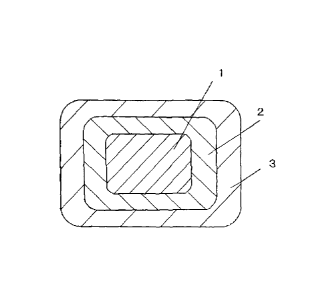
1
INVERTER SURGE-RESISTANT INSULATED WIRE
TECHNICAL FIELD
{0001}
The present invention relates to an inverter surge-resistant insulated wire.
BACKGROUND ART
{0002}
Inverters have been employed in many types of electrical equipments, as an
efficient variable-speed control unit. Inverters are switched at a frequency
of
several kHz to tens of kHz, to cause a surge voltage at every pulse thereof.
Inverter surge is a phenomenon in which reflection occurs at a breakpoint of
impedance, for example, at a starting end, a termination end, or the like of a
connected wire in the propagation system, followed by applying a voltage twice
as
high as the inverter output voltage at the maximum. In particular, an output
pulse
occurred due to a high-speed switching device, such as an IGBT, is high in
steep
voltage rise. Accordingly, even if a connection cable is short, the surge
voltage is
high, and voltage decay due to the connection cable is also low. As a result,
a
voltage almost twice as high as the inverter output voltage occurs.
{0003}
As coils for electrical equipments, such as inverter-related equipments, for
example, high-speed switching devices, inverter motors, and transformers,
insulated wires made of enameled wires are mainly used as magnet wires in the
coils. Further, as described above, since a voltage almost twice as high as
the
inverter output voltage is applied in inverter-related equipments, it has
become
required to minimize the inverter surge deterioration of the enameled wire,
which is
one of the materials constituting the coils of those electrical equipments.
CA 02867657 2016-12-20
2
{0004}
In the meantime, partial discharge deterioration is a complicated
phenomenon in which an electrical-insulation material undergoes, for example,
molecular chain breakage deterioration caused by collision with charged
particles
that have been generated by partial discharge of the insulating material,
sputtering
deterioration, thermal fusion or thermal decomposition deterioration caused by
local
temperature rise, and chemical deterioration caused by ozone generated due to
discharge. For this reason, reduction in thickness, for example, is observed
in the
electrical-insulation materials, which have been deteriorated as a result of
actual
partial discharge.
{0005}
It has been believed that inverter surge deterioration of an insulated wire
also proceeds by the same mechanism as in the case of general partial
discharge
deterioration. Namely, inverter surge deterioration of an enameled wire is a
phenomenon in which partial discharge occurs in the insulated wire due to the
surge
voltage with a high peak value, which is occurred at the inverter, and the
coating of
the insulated wire causes partial discharge deterioration as a result of the
partial
discharge; in other words, the inverter surge deterioration of an insulated
wire is
high-frequency partial discharge deterioration.
{0006}
Insulated wires that are able to withstand several hundred volts order of
surge voltage have been required for the recent electrical equipment. That is,
there is a demand for insulated wires that have a partial discharge inception
voltage
of several hundred volts order or more. Herein, the partial discharge
inception
voltage is a value that is measured by a commercially available apparatus
called
partial discharge tester. Measurement temperature, frequency of the
alternating
current voltage to be used, measurement sensitivity, and the like are values
that
may vary as necessary, but the above-mentioned value is an effective value of
the
i
II
CA 02867657 2016-12-20
3
voltage at which partial discharge occurs, which is measured at 25 C, 50 Hz,
and
pC.
When the partial discharge inception voltage is measured, a method is used
in which the most severe condition possible in the case where the insulated
wire is
5 used as a magnet wire is envisaged, and a specimen shape is formed which
can be
observed in between two closely contacting insulated wires. For example, in
the
case of an insulated wire having a circular cross-section, two insulated wires
are
brought into linear contact by spiral twisting the wires together, and a
voltage is
applied between the two insulated wires. Alternatively, in the case of an
insulated
10 wire having a rectangular cross-section, use is made of a method of
bringing two
insulated wires into planar contact through the planes, which are the long
sides of
the insulated wires, and applying a voltage between the two insulated wires.
{0007}
In order to obtain an insulated wire that does not cause partial discharge,
that is, having a high partial discharge inception voltage, so as to prevent
the
deterioration of the enamel layer of the insulated wire caused by the partial
discharge, it is thought to utilize a method of using a resin having a low
dielectric
constant in the enamel layer or increasing the thickness of the enamel layer.
However, the resins of commonly used resin varnishes generally have a
dielectric
constant between 3 and 5, and none of the resins have particular low
dielectric
constant. Further, upon considering other properties (heat resistance, solvent
resistance, flexibility, and the like) required from the enamel layer, it is
not
necessarily possible to select actually a resin having a low dielectric
constant.
Therefore, in order to obtain a high partial discharge inception voltage, it
is
indispensable to increase the thickness of the enamel layer. When the resins
having a dielectric constant of 3 to 5 are used in the enamel layer, if it is
intended to
obtain a targeted partial discharge inception voltage of 1 kVp or higher (a
high peak
value), it is necessary based on the experience to set the thickness of the
enamel
11
CA 02867657 2016-12-20
4
layer at 60 pm or more.
{0008}
However, to thicken the in enameled layer, the number of times for passing
through a baking furnace increases in a production process thereof, whereby
making a film composed of copper oxide on a copper conductor surface thicker,
this
in turn, causing lowering in adhesion between the conductor and the backed
enamel layer. For example, in the case of obtaining an enamel layer with
thickness 60 pm or more, the number of passages through the baking furnace
exceeds 12 times. It has been known that if this number of passages exceeds 12
times, the adhesive force between the conductor and the enamel layer is
conspicuously lowered.
It is also thought to utilize a method of increasing the thickness that can be
formed by a single baking step, in order not to increase the number of
passages
through the baking furnace. However, this method has a drawback that the
solvent
of the varnish is not completely vaporized and remains in the enamel layer as
voids.
{0009}
Further, it has become demanded to further improve various performances,
such as heat resistance, mechanical properties, chemical properties,
electrical
properties, and reliability, in the electrical equipments developed in recent
years, as
compared to the conventional electrical equipments. Under the situations,
excellent insulation property at high temperature and thermal aging resistance
property as well as above-mentioned high partial discharge inception voltage
have
become required from insulated wires, such as enameled wires, that are used as
magnet wires for electrical equipments for aerospace use, electrical
equipments for
aircraft, electrical equipments for nuclear power, electrical equipments for
energy,
and electrical equipments for automobiles.
To these problems, an attempt to provide a coated resin at the outer side of
the enamel wire has been made (Patent Literatures 1 and 2). However, the
i
CA 02867657 2016-12-20
insulated wires described in Patent Literatures 1 and 2 also still have room
to
improve a partial discharge inception voltage, insulation property at a high
temperature, and a thermal aging resistance property. Further, Patent
Literature 3
is cited as a technique for improving the partial discharge inception voltage.
5
CITATION LIST
PATENT LITERATURES
{0010}
Patent Literature 1: JP-B-7-031944 ("JP-B" means examined Japanese
patent publication)
Patent Literature 2: JP-A-63-195913 ("JP-A" means unexamined published
Japanese patent application)
Patent Literature 3: JP-A-2005-203334
SUMMARY OF INVENTION
TECHNICAL PROBLEM
{0011}
The present invention is contemplated for providing an inverter surge-
resistant insulated wire in which an insulation layer is made thick without
deterioration of insulation property at a high temperature, and which has high
partial
discharge inception voltage and excellent thermal aging resistance property.
SOLUTION TO PROBLEM
{0012}
The present inventors, as a result of intensive studies for dissolving the
above-described problems, have found that in the insulated wire provided with
an
extrusion-coated resin layer at the outer side of the enamel layer thereof,
any of the
partial discharge inception voltage, the insulation property at a high
temperature,
CA 02867657 2016-12-20
6
and the thermal aging resistance property can be improved by setting specific
ranges for an individual thickness and a total thickness of the enamel layer
and the
extrusion-coated resin layer, and the minimum of tensile elastic modulus of
the
extrusion-coated resin layer at a range of 25 to 250 C, and further by setting
specific ranges for an individual dielectric constant of an insulation layer
composed
of a combination of the enamel layer and the extrusion-coated resin layer at
25 C
and at 250 C, and a ratio of the specific permittivities at 250 C. The present
invention has been made on a basis of this knowledge.
{0013}
The above-described problems can be solved by the following means.
(1) An inverter surge-resistant insulated wire, having at least one
baked enamel
layer around the outer periphery of a conductor, and an extrusion-coated resin
layer
at the outside of the baked enamel layer,
wherein the extrusion-coated resin layer is a single layer, and a resin of the
resin layer is a resin selected from polyether ether ketone, a thermoplastic
polyimide, a polyamide having an aromatic ring, a polyester having an aromatic
ring,
and polyketone,
wherein a total thickness of the baked enamel layer and the extrusion-
coated resin layer is 50pm or more, a thickness of the baked enamel layer is
60pm
or less, and a thickness of the extrusion-coated resin layer is 200pm or less,
wherein the minimum of tensile elastic modulus of the extrusion-coated
resin layer at a range of 25 to 250 C is 100MPa or more and 400MPa or less,
wherein a dielectric constant of an insulation layer having a combination of
the baked enamel layer and the extrusion-coated resin layer is 3.0 or more and
3.5
or less at 25 C and 4.0 or more and 5.0 or less at 250 C, and
wherein a relation between dielectric constant (El') of the baked enamel
layer at 250 C and dielectric constant (E2') of the extrusion-coated resin
layer at
250 C satisfies 2.0 (E27E1')>1.
CA 02867657 2016-12-20
7
(2) The inverter surge-resistant insulated wire as described in the above
item
(1), wherein the extrusion-coated resin layer is a layer formed by polyether
ether
ketone.
(3) The inverter surge-resistant insulated wire as described in the above
item
(1) or (2), wherein the conductor has a rectangular cross-section.
(4) The inverter surge-resistant insulated wire as described in any one of
the
above items (1) to (3), wherein the thickness of the backed enamel layer is
40pm or
less.
{0014}
In this Description, the term "dielectric constant of an insulation layer"
means an effective dielectric constant of an insulation layer in the inverter
surge-
resistant insulated wire, and further means a value calculated by the
following
formula from both capacitance of the inverter surge-resistant insulated wire
measured by the method described below and outside diameters of the conductor
and the insulated wire.
{0015}
Formula: Er*=Cp=Log(b/a) / (21TE0)
{0016}
Herein, Er* represents a dielectric constant of the insulation layer, Cp
represents a capacitance per unit length [pF/m], a represents an outside
diameter of
the conductor, b represents an outside diameters of the insulated wire, co
represents
a vacuum permittivity (8.855x10⁻¹²[F/m]).
Also note that in a case where the cross-section of the inverter surge-
resistant insulated wire is not circular but rectangular as an example, "the
dielectric
constant of the insulation layer" can be calculated using a relation that
capacitance
Cp of the insulation layer is a sum of capacitance Cf of a flat part and
capacitance
Ce of a corner part (Cp=Cf+Ce). Specifically, provided that lengths of a long
side
and a short side of the straight-line portion of the conductor are represented
by Li
II
CA 02867657 2016-12-20
8
and L2, respectively, a radius of curvature of the conductor corner is
represented by
R, and a thickness of the insulation layer is represented by T, the
capacitance Cf of
the flat part and the capacitance Ce of the corner part are expressed by the
following formulae. Using these formulae, Er* can be calculated from the
observed
capacitance of the insulated wire and capacitance Cp (Cf+Ce) of the insulation
layer.
{0017}
Cf=(Er*/E0)x2x(L1+L2)/T
Ce=(Er*/E0)x2-rrEo/Log{(R+T)/R}
ADVANTAGEOUS EFFECTS OF INVENTION
{0018}
The inverter surge-resistant insulated wire of the present invention has high
partial discharge inception voltage and is excellent in both insulation
property at a
high temperature and thermal aging resistance property.
Other and further features and advantages of the invention will appear more
fully from the following description, appropriately referring to the
accompanying
drawings.
BRIEF DESCRIPTION OF THE DRAWINGS
{0019}
{Fig. 1}
Fig. 1 is a cross-sectional view showing an embodiment of the inverter
surge-resistant insulated wire of the present invention.
{Fig. 2}
Fig. 2 is a cross-sectional view showing another embodiment of the inverter
surge-resistant insulated wire of the present invention.
i 1
CA 02867657 2016-12-20
9
MODE FOR CARRYING OUT THE INVENTION
{0020}
The present invention has at least one baked enamel layer around the outer
periphery of a conductor, and at least one extrusion-coated resin layer at the
outside thereof, and satisfies the following conditions (1) to (6):
(1) the total thickness of the baked enamel layer and the extrusion-coated
resin
layer is 50pm or more;
(2) the thickness of the baked enamel layer is 60pm or less;
(3) the thickness of the extrusion-coated resin layer is 200pm or less;
(4) the minimum of tensile elastic modulus of the extrusion-coated resin
layer at
a range of 25 to 250 C is 100MPa or more;
(5) the effective dielectric constant of the insulation layer having a
combination
of the baked enamel layer and the extrusion-coated resin layer is 3.5 or less
at 25 C
and 5.0 or less at 250 C; and
(6) the relation between dielectric constant (El') of the baked enamel
layer at
250 C and dielectric constant (E2') of the extrusion-coated resin layer at 250
C
satisfies (E2'/E1')>1.
The inverter surge-resistant insulated wire of the present invention which
has such features has high partial discharge inception voltage and is
excellent in
both insulation property at a high temperature and thermal aging resistance
property.
Therefore, the inverter surge-resistant insulated wire of the present
invention (hereinafter, referred to simply as "insulated wire") is preferably
suitable
for heat-resistant winding wires, and can be used for various purposes as
described
below.
{0021}
The embodiments of an inverter surge-resistant insulated wire of the
present invention will be explained, with reference to the drawings.
CA 02867657 2016-12-20
One embodiment of the inverter surge-resistant insulated wire of the
present invention, shown in FIG. 1 has a conductor 1 having a circular cross-
section,
one baked enamel layer 2 covering the circumferential outer side of the
conductor 1,
and one extrusion-coated resin layer 3 covering the circumferential outer side
of the
5 baked enamel layer 2, and the cross-section of the entire inverter surge-
resistant
insulated wire has a circular shape.
Another embodiment of the inverter surge-resistant insulated wire of the
present invention, shown in FIG. 2 has a conductor 1 having a rectangular
cross-
section, one baked enamel layer 2 covering the outer periphery of the
conductor 1,
10 and one extrusion-coated resin layer 3 covering the outer periphery of
the baked
enamel layer 2, and the cross-section of the entire inverter surge-resistant
insulated
wire has a rectangular shape.
{0022}
In another embodiment, a total thickness of the baked enamel layer and the
extrusion-coated resin layer is enough to be at least one of the total
thicknesses of
the baked enamel layer and the extrusion-coated resin layer provided
respectively
at two sides and at the other two sides, in which the two sides are opposed to
each
other in the rectangular cross-section. In this embodiment, if the total
thickness of
the extrusion-coated resin layer and the baked enamel layer formed at the two
sides
in which discharge occurs is a predetermined thickness, a partial discharge
inception voltage can be maintained although the total thickness of the layers
formed at the other two sides is thinner than the former, and for example, a
rate of
the total cross-sectional area of the conductor with respect to the total
cross-
sectional area in a slot of the motor (space factor) can also be increased.
Therefore, the total thicknesses of the extrusion-coated resin layer and the
baked
enamel layer provided respectively at two sides and at other two sides may be
of
any thickness as long as the two sides in which discharge occurs, that is to
say, at
least one of them is 50 pm or more, and preferably each of the two sides and
the
I]
CA 02867657 2016-12-20
11
other two sides is 50 pm or more.
As for the total thickness, the two sides may be the same or different from
one another and it is preferable that they are different from one another in
the
following manner from the standpoint of the space factor with respect to the
stator
slot. Specifically, the partial discharge that occurs in the stator slot such
as a
motor can be divided into two classes of a case where a partial discharge
occurs
between a slot and a wire and a case where a partial discharge occurs between
a
wire and a wire. As a result, a rate of the total cross-sectional area of the
motor
with respect to the total cross-sectional area in a slot of the motor (space
factor) can
be increased while maintaining the value of partial discharge inception
voltage, by
using an insulated wire in which the thickness of the extrusion-coated resin
layer
provided at a flat surface is different from the thickness of the extrusion-
coated resin
layer provided at an edge surface of the insulated wire.
{0023}
Here, the flat surface refers to a pair of the long side of two pairs of the
two
sides that oppose in a rectangular cross-section of the flat wire, while the
edge
surface refers to a pair of the short side of two pairs of the two sides that
oppose.
In a case where a discharge occurs between a slot and a wire when wires
which are different from one another in terms of the thickness in the edge
surface
and the flat surface are arranged in a row in a slot, they are arranged so
that thick
film surfaces contact with each other with respect to the slot, and they are
arranged
so that thin film surfaces of the neighboring wires contact with each other.
The
thinner the film thickness is, the more the number of wires can be inserted
and
space factor is increased. Besides, in this time, the value of a partial
discharge
inception voltage can be maintained. Similarly, in a case where discharge is
easy
to occur between a wire and a wire, if the surface having a thick film
thickness is
arranged so as to be a surface to contact with a wire whereas the surface
which
faces the slot is made thin, the space factor is increased because a size of
the slot
i
CA 02867657 2016-12-20
12
is not increased more than necessary. Besides, in this time, the value of a
partial
discharge inception voltage can be maintained.
In a case where the thickness of the extrusion-coated resin layer is different
between a pair of two sides which are opposed to each other and a pair of the
other
two sides which are opposed to each other in the cross section, when provided
that
the thickness of the pair of two sides which are opposed to each other is 1,
the
thickness of the pair of the other two sides which are opposed to each other
is
preferably adjusted to a range of 1.01 to 5, and more preferably adjusted to a
range
of 1.01 to 3.
{0024}
The foregoing one preferable embodiment and another preferable
embodiment (hereinafter collectively referred to as the embodiments of the
present
invention) are explained collectively because these are basically similar
except that
the shape of the cross-section of both the conductor and the inverter surge-
resistant
insulated wire is different from one another.
{0025}
(Conductor)
As the conductor used in the insulated wires of the present invention, use
may be made of any conductor that has been conventionally used in insulated
wires.
The conductor is a conductor of preferably a low-oxygen copper whose oxygen
content is 30 ppm or less, and more preferably a low-oxygen copper whose
oxygen
content is 20 ppm or less or oxygen-free copper. When the conductor is melted
by
heat for the purpose of welding if the oxygen content is 30 ppm or less, voids
caused by contained oxygen are not occurred at a welded portion, the
deterioration
of the electrical resistance of the welded portion can be prevented, and the
strength
of the welded portion can be secured.
As shown in FIG. 1 and FIG. 2, a conductor, which has a desired transverse
cross-sectional shape, may be used, and in terms of space factor with respect
to
CA 02867657 2016-12-20
13
the stator slot, it is preferable to use a conductor having a cross-sectional
shape
except for a circular shape, and as shown in FIG. 2, particularly preferable
to use a
rectangular conductor. Furthermore, in terms of suppressing partial discharge
from corners, it is preferable that chamfers (radius r) are formed at four
corners.
{0026}
(Baked enamel layer)
The baked enamel layer (hereinafter, may be referred to simply as "enamel
layer") 2 is formed by an enamel resin into at least one layer which may be a
single
layer or a multilayer. As the enamel resin that forms the enamel layer, any of
those conventionally utilized can be put to use, and examples include
polyimide,
polyamideimide, polyesterimide, polyetherimide, polyimide hydantoin-modified
polyester, polyamide, formal, polyurethane, polyester, polyvinylformal, epoxy,
and
polyhydantoin. As the enamel resin, polyimide-based resins, such as polyimide,
polyamideimide, polyesterimide, polyetherimide, and polyimide hydantoin-
modified
polyester, which are excellent in heat resistance is preferable. Of them,
polyamideimide and polyimide are more preferable, and polyamideimide is
particularly preferable.
{0027}
As for the enamel resin for forming the enamel layer, it is preferable that
the
dielectric constant El at 25 C is small, on the standpoint that a partial
discharge
inception voltage can be increased. For example, the dielectric constant El is
preferably 5.0 or less, and more preferably 4.0 or less. The lower limit of
the
dielectric constant El is not limited in particular, and preferably 3.0 or
more in
practice.
Further, as for the enamel resin, in addition to the dielectric constant El at
25 C which is in the above-described range, it is preferable that the
dielectric
constant El' at 250 C is 6.0 or less, and more preferably 5.0 or less, from
the
standpoint that excellent insulation property can be exerted even at a high
CA 02867657 2016-12-20
14
temperature. The lower limit of the dielectric constant El' is not limited in
particular,
and preferably 3.0 or more in practice.
The specific permittivities El and El' of the enamel resin can be measured
at a measuring temperature of 25 C or 250 C respectively, using a commercially
available dielectric measuring-equipment. The measuring temperature and the
frequency are changed as needed; however, in the present invention, the
dielectric
constant means a value measured at 100Hz, unless described otherwise.
{0028}
Therefore, the enamel resin is selected from the above-described resins in
consideration of the specific permittivities El and El' or the like. For
example, as
commercially available enamel resins which satisfy the specific permittivities
El and
El', it is possible to use a polyamideimide resin (PAI) varnish (manufactured
by
Hitachi Chemical Co., Ltd., trade name: H1406) having dielectric constant El
of 3.9
and dielectric constant El' of 4.4, a polyimide resin (PI) varnish
(manufactured by
Unitika Ltd., trade name: U IMIDE) having dielectric constant El of 3.5 and
dielectric
constant El' of 4.0, and the like. The enamel resin may be used solely or in
mixture of two or more kinds. Additives may be added within the above-
described
ranges.
{0029}
From the standpoint that even if a thickness of the enamel layer is made
thick whereby a high-partial discharge inception voltage can be attained, the
number of passages through a baking furnace can be reduced when the enamel
layer is formed, and adhesion between the conductor and the enamel layer can
be
prevented from being extremely lowered, and that the occurrence of the voids
can
be prevented, the thickness of the enamel layer is 60 im or less, preferably
50 jtm
or less, more preferably 45 pm or less, and particularly preferably 40 p.m or
less.
Further, in order to prevent deterioration of voltage resistance or heat
resistance,
which are properties required for the enameled wires as insulated wires, it is
CA 02867657 2016-12-20
preferable that the enamel layer has a certain thickness. The thickness of the
enamel layer is not particularly limited, as long as it is a thickness where
no
pinholes are formed. The thickness of the enamel layer is preferably 3 i_tm or
more,
and more preferably 6 jim or more. In another embodiment shown in FIG. 2, each
5 of the thicknesses of the enamel layers provided respectively at two
sides and at
the other two sides is adjusted to 60 jim or less.
{0030}
The backed enamel layer can be formed, by coating of a resin varnish
containing the above-mentioned the enamel resin onto a conductor and baking of
10 the resin varnish, each of which is preferably made several times. A
method of
coating the resin varnish may be a usual manner. Examples of the method
include
a method using a die for coating varnish, which has a shape similar to the
shape of
a conductor, or a method using a die called "universal die" that is formed in
the
shape of a curb when the conductor has a quadrangular cross-section. The
15 conductor to which the resin varnish is coated is baked in a baking
furnace in a
usual manner. Specific baking conditions depend on the shape of the furnace to
be used. In the case of using a natural convection-type vertical furnace with
length
approximately 5 m, baking may be achieved by setting a transit time of 10 to
90 sec
at 400 to 500 C.
{0031}
(Extrusion-coated resin layer)
In order to obtain an insulated wire having a high partial discharge inception
voltage, at least one extrusion-coated resin layer is provided around the
outer side
of the baked enamel layer. The extrusion-coated resin layer may be a single
layer
or multilayers.
Further in the present invention, in a case where the extrusion-coated resin
layer is composed of multilayers, it is preferable that the same resin among
the
multilayers is used. Specifically, layers formed by the same resin as the
resin
CA 02867657 2016-12-20
16
contained in the extrusion-coated resin layer nearest the enamel layer side
are
laminated. Here, the presence or absence of additives other than the resin,
and
the kind or the compounding amount thereof may be different from one another
among the multilayers, as long as the resin is the same. In the present
invention,
the extrusion-coated resin layer is preferably a single layer or double
layers, and a
single layer is particularly preferable.
Herein, the single layer means that even in a case where layers in which
resins forming the layers and additives contained therein are the same in each
of
the layers, are laminated, these layers are regarded as the same layer, and on
the
other hand, even in a case that the layers are composed of the same resins,
when
compositions constituting the layers are different from one another such that,
for
example, a kind of additives or a compounding amount is different from one
another,
the number of the layers are counted.
This definition is also applied to layers other than the extrusion-coated
resin
layer.
{0032}
The extrusion-coated resin layer is a layer of a thermoplastic resin.
Examples of the thermoplastic resin for forming the extrusion-coated resin
layer
include polyether ether ketone (PEEK). Here, the polyether ether ketone means
inclusion of modified polyether ether ketone (modified-PEEK). The modified
polyether ether ketone is polyether ether ketone denatured by adding thereto
an
auxiliary agent or a resin which is used for improving mechanical properties
or
thermal properties. Examples of the foregoing modified polyether ether ketone
include products under the trade name "AvaSpire" series, specifically
"AvaSpire AV-
650" (trade name, manufactured by Solvay Specialty Polymers).
Furthermore, Examples of thermoplastic resin include thermoplastic
polyimide (PI), aromatic polyamide having aromatic ring (referred as aromatic
polyamide), polyester having aromatic ring (referred as aromatic polyester),
CA 02867657 2016-12-20
17
polyketone (PK), and polyetylene naphtalate (PEN).
{0033}
In the extrusion-coated resin layer, among them, polyether ether ketone
(PEEK include modified polyether ether ketone), thermoplastic polyimide (PI),
aromatic polyamide having aromatic ring (referred as aromatic polyamide),
polyester having aromatic ring (referred as aromatic polyester), polyketone
(PK), or
polyetylene naphtalate (PEN) is preferable, polyether ether ketone (PEEK
include
modified polyether ether ketone), or polyetylene naphtalate (PEN) is more
preferable, polyether ether ketone (PEEK include modified polyether ether
ketone)
is further more preferable, polyether ether ketone not including modified
polyether
ether ketone (PEEK) is particularly preferable.
{0034}
The extrusion-coated resin for forming the extrusion-coated resin layer may
be an extrusion-moldable thermoplastic resin. As for the extrusion-coated
resin, it
is preferable that the dielectric constant 2 at 25 C is small, on the
standpoint that a
partial discharge inception voltage can be increased. For example, the
dielectric
constant 2 is preferably 5.0 or less, and more preferably 4.0 or less. The
lower
limit of the dielectric constant 2 is not limited in particular, and
preferably 2.0 or
more in practice.
Further, as for the thermoplastic resin, in addition to the dielectric
constant
2 at 25 C which is in the above-described range, it is preferable that the
dielectric
constant 2' at 250 C is 6.0 or less, and more preferably 5.0 or less, from
the
standpoint that excellent insulation property can be exerted even at a high
temperature. The lower limit of the dielectric constant 2' is not limited in
particular,
and preferably 2.0 or more in practice.
The specific permittivities 2 and 2' of the enamel resin can be measured
at a measuring temperature of 25 C or 250 C respectively, using a commercially
available dielectric measuring-equipment. The measuring temperature and the
CA 02867657 2016-12-20
18
frequency are changed as needed; however, in the present invention, the
dielectric
constant means a value measured at 100Hz, unless described otherwise.
{0035}
On the standpoint that the extrusion-coated resin layer, more specifically the
thermoplastic resin for forming the extrusion-coated resin layer is able to
exert
excellent mechanical properties under the conditions ranging from low
temperature
like room temperature to a high temperature, and excellent insulation property
at a
high temperature, it is preferable that the minimum of the tensile elastic
modulus in
the temperature range of 25 to 250 C is 100MPa or more, and the minimum of the
tensile elastic modulus even in the temperature range of from more than 250 C
to
280 C or less is maintained to be 100MPa or more. Thus, tensile elastic
modulus
of the thermoplastic resin is 100MPa or more in the temperature range of 25 C
to
250 C, and more preferably in the temperature range of 25 C to 280 C. The
minimum of the tensile elastic modulus is preferably 200MPa or more, and more
preferably 300MPa or more, and the upper limit (maximum) thereof is not
limited in
particular, and preferably 400MPa in practice. The tensile elastic modulus can
be
adjusted by degree of cross-linkage of the thermoplastic resin, crystallinity,
and the
like.
The tensile elastic modulus can be measured by dynamic viscoelasticity
measurement (DMS). Specifically, measurement is carried out continuously or
intermittently in a temperature range of 25 C to 280 C, by using a tensile
mode,
frequency of 10 Hz and strain amount of 1/1000, while changing a measuring
temperature at an elevating rate of 5 C/min. The control mode at the time of
measurement, the frequency, the strain amount, the measuring temperature and
the
like is changeable, if needed.
{0036}
In a case where the thermoplastic resin is a crystalline thermoplastic resin,
enhancement of crystallinity of the film is preferable on the standpoint that
a rapid
i
CA 02867657 2016-12-20
19
decline in the tensile elastic modulus in the vicinity of a glass transition
temperature
can be suppressed, and both excellent mechanical properties under the
conditions
of from a low temperature to a high temperature and excellent insulation
properties
at a high temperature can be exerted. Specifically, the crystallinity of the
film is
preferably 50% or more, more preferably 70% or more, and particularly
preferably
80% or more. The upper limit of the crystallinity is not limited in
particularly, and
for example it is 100%. The film crystallinity of the extrusion-coated resin
layer can
be measured using differential scanning calorimetry (DSC). Specifically, an
adequate amount of a film of the extrusion-coated resin layer is weighed and
temperature thereof is elevated at the rate of 5 C/min. During this stage, a
heat
amount (melting heat amount) due to melting that is observed at the region
more
than 300 C and a heat amount (crystallization heat amount) due to
crystallization
that is observed at round 150 C are calculated and a difference of the heat
amount
in which the crystallization heat amount is deducted from the melting heat
amount,
with respect to the melting heat amount is defined as the film crystallinity.
This
calculation formula is shown below.
{0037}
Calculation formula: the film crystallinity (`)/0) = [(the melting heat amount
- the
crystallization heat amount) / (the melting heat amount)] x 100
{0038}
Further, on the standpoint that the thermal aging resistance is improved
much more, a melting point of the thermoplastic resin for forming the
extrusion-
coated resin layer is preferably 260 C or more, more preferably 280 C or more,
and
particularly preferably 330 C or more. The melting point of the thermoplastic
resin
is, for example, preferably 370 C or less, and more preferably 360 C or less.
The
melting point of the thermoplastic resin can be measured by the method
described
below using differential scanning calorimetry (DSC). Specifically, temperature
of
10mg of the extrusion-coated resin layer is elevated at the rate of 5 C/min
using
CA 02867657 2016-12-20
thermal analysis equipment "DSC-60" (manufactured by Shimadzu Corporation),
and during this stage, a peak temperature of the heat amount due to melting
that is
observed at the region more than 250 C is read and defines as a melting point.
Also note that when there is a plurality of peak temperatures, the peak
temperature
5 of higher temperature is defined as a melting point.
{0039}
The thermoplastic resin for forming the extrusion-coated resin layer is
selected from the above-described thermoplastic resin by considering the
dielectric
constant E2 at 25 C, the dielectric constant E2' at 250 C, the minimum of
tensile
10 elastic modulus in a range of 25 to 250 C, and if needed, the melting
point or the
like. In particular, preferred are thermoplastic resins in which the
individual
thickness and the total thickness of the enamel layer and the extrusion-coated
resin
layer, the specific permittivities of the insulation layer at 25 C and at 250
C, the ratio
of the above-described specific permittivities, and the minimum of tensile
elastic
15 modulus in a range of 25 to 250 C each fall within the above-described
ranges; for
example, preferred are at least one of thermoplastic resins selected from the
group
consisting of polyether ether ketone and a modified polyether ether ketone.
That is,
the extrusion-coated resin layer is preferably a polyether ether ketone-based
layer.
If these thermoplastic resins is used as the thermoplastic resin for forming
the
20 extrusion-coated resin layer, a partial discharge inception voltage is
improved much
more, both a mechanical property under the conditions of from a low
temperature to
a high temperature and an insulation property at a high temperature are also
maintained at a high level, and in addition a thermal aging resistance
property is
also improved much more, by combined with the above-described individual
thickness, total thickness and specific permittivities, the above-described
specific
permittivities and ratio of the minimum of tensile elastic modulus in a range
of 25 to
250 C. As these thermoplastic resins, it is possible to use, for example,
polyether
ether ketone (PEEK) having dielectric constant a of 3.1 and dielectric
constant E2'
i
CA 02867657 2016-12-20
21
of 4.7 (manufactured by Solvay Specialty Polymers, trade name:"KetaSpire KT-
820") and the like.
The thermoplastic resin for forming the extrusion-coated resin layer may be
used singly alone, or two or more kinds thereof. Also note that the
thermoplastic
resin may be blended with other resins, elastomers or the like, if not
extended
beyond the above-described range or the range described below of the minimum
of
tensile elastic modulus in a range of 25 to 250 C and the specific
permittivities.
{0040}
The thickness of the extrusion-coated resin layer is less than 200 pm, and
the thickness of less than 180 pm is preferable. If the thickness of the
extrusion-
coated resin layer is too thick, when an insulated wire is wound around an
iron core
and heated, a whitened portion is sometimes formed on the insulated wire
surface.
As just described, if the extrusion-coated resin layer is too thick,
flexibility suitable
for an insulated wire becomes poor because the extrusion-coated resin layer
itself
has stiffness, and as a result, the poor flexibility sometimes has an effect
on a
change of the electrical insulation keeping property before and after the
working.
On the other hand, the thickness of the extrusion-coated resin layer is
preferably
5pm or more, and more preferably 15pm or more, from the standpoint that
insulation failure can be prevented. In above-mentioned another embodiment,
each of the thicknesses of the extrusion-coated resin layers provided
respectively at
two sides and at the other two sides is adjusted to 200 ttm or less.
{0041}
The extrusion-coated resin layer can be formed by extrusion-molding the
above-described thermoplastic resin on an enamel layer having been formed on a
conductor. The conditions at the time of extrusion-molding, for example, a
condition of extrusion temperature are set appropriately according to the
thermoplastic resin to be used. Taking an example of preferable extrusion
temperatures, specifically the extrusion temperature is set at a temperature
higher
II
CA 02867657 2016-12-20
22
by 30 C than the melting point, preferably about 40 C to 60 C than the melting
point
in order to achieve a melt viscosity suitable for the extrusion-coating. If
the
extrusion-coated resin layer is formed by the extrusion-molding as just
described,
there is no need to pass it through a baking furnace at the time of forming a
coated
resin layer in the production process. As a result, there is an advantage that
a
thickness of an insulation layer, namely the extrusion-coated resin layer can
be
made thick without growing the thickness of an oxidation-coated layer of the
conductor.
{0042}
In the preferable embodiments, a total thickness of the enamel layer and the
extrusion-coated resin layer is 50 pm or more. If the total thickness is 50 pm
or
more, the partial discharge inception voltage of the insulated wire becomes
lkVp or
more, thereby being able to prevent the inverter surge deterioration. This
total
thickness is preferably 75 pm or more, and more preferably 100 pm or more from
the standpoint that this allows development of higher partial discharge
inception
voltage and a high level of prevention of inverter surge deterioration. In
another
embodiment described above, the total thicknesses of the baked enamel layer
and
the extrusion-coated resin layer provided respectively at two sides and at the
other
two sides are each 50pm or more. Thus, if a thickness of the enamel layer is
adjusted to 60pm or less, a thickness of the extrusion-coated resin layer is
adjusted
to 200pm or less, and a total thickness of the enamel layer and the extrusion-
coated
resin layer is adjusted to 50pm or more, at least a partial discharge
inception
voltage of the insulated wire, that is, prevention of inverter surge
deterioration,
adhesive strength between the conductor and the enamel layer, and suppression
of
foaming during making of the enamel layer can be satisfied. Also note that the
total thickness of the baked enamel layer and the extrusion-coated resin layer
is
preferably 260pm or less, and preferably 200pm or less in order that working
can be
done keeping out of trouble in view of the properties of insulation retention
before
1 i
CA 02867657 2016-12-20
23
and after coil-working (hereinafter, referred to as insulation retention
properties
before and after working).
{0043}
Therefore, in the insulated wire of the embodiments of the present invention,
a conductor and an enamel layer adhere to each other with a strong adhesive
strength. The adhesive strength between the conductor and the enamel layer can
be evaluated, for example, in terms of rotation frequency until occurring of
the float
of the enamel layer, in accordance with the same way as described in the JIS C
3003 Methods of test for enamel wires, Section 8. Adhesiveness, 8.1 b) Torsion
methods. Also for the rectangular wire having a square-shaped cross-section,
evaluation can be carried out similarly. In the present invention, those in
which the
rotation frequency until float of the enamel layer occurs is 15 rounds or more
is
judged as being good in terms of adhesiveness, and the insulated wire
according to
this preferable embodiment achieves 15 rounds or more of rotation frequency.
{0044}
In the embodiments of the present invention, the dielectric constant of the
entire insulation layer having a combination of the baked enamel layer and the
extrusion-coated resin layer is 3.5 or less at 25 C. If the dielectric
constant is 3.5
or less, at least a partial discharge inception voltage of the insulated wire
at 25 C
can be improved to lkVp or more whereby inverter surge deterioration can be
prevented. The dielectric constant at 25 C is preferably 3.2 or less on the
standpoint that the inverter surge deterioration can be prevented still more.
The
lower limit is not limited in particular; and, preferably 3.0 or more in
practice.
Further, the dielectric constant of the entire insulation layer having a
combination of the baked enamel layer and the extrusion-coated resin layer is
5.0 or
less at 250 C. Generally, the permittivity of the resin increases at high
temperature, and the partial discharge inception voltage naturally reduces in
association with reduction in density of air. However, if the dielectric
constant is
CA 02867657 2016-12-20
24
5.0 or less at 250 C, reduction of the partial discharge inception voltage at
a high
temperature, for example, at 250 C can be suppressed. The dielectric constant
at
250 C is preferably 4.8 or less on the standpoint that reduction of the
partial
discharge inception voltage can be prevented still more. The lower limit is
not
limited in particular; and, preferably 4.0 or more in practice.
{0045}
The specific permittivities of the entire insulation layer at 25 C and at 250
C
can be adjusted to the above-described ranges by selecting specific
permittivities El
and El' and a thickness of the enamel resin for forming the enamel layer, and
specific permittivities E2 and E2' and a thickness of the thermoplastic resin
for
forming the extrusion-coated resin layer. For example, if the enamel resin
having
small specific permittivities El and El' and/or the thermoplastic resin having
small
specific permittivities E2 and E2' are selected, the dielectric constant of
the entire
insulation layer can be made small. Further, if the resin having smaller
dielectric
constant is coated thicker, the dielectric constant of the entire insulation
layer can
be made small.
{0046}
The dielectric constant of the entire insulation layers can be calculated by
formula as described above from both capacitance of the inverter surge-
resistant
insulated wire measured by the method described below and outside diameters of
the conductor and the insulated wire.
By using both a LCR HITESTER (Model 3532-50 (trade name: LCR
HITESTER) manufactured by HIOKI E.E. CORPORATION) and an insulated wire
left for 24 hours in a dry air at ordinary temperature (25 C), and setting a
measuring
temperature to 25 C and 250 C, and putting the insulated wire into a
thermostat
bath having been set to a predetermined temperature, and then measurement of
capacitance is carried out at the time when the temperature has become
constant.
{0047}
CA 02867657 2016-12-20
In the embodiments of the present invention, a relation between dielectric
constant El' of the enamel layer at 250 C and dielectric constant E2' of the
extrusion-coated resin layer at 250 C satisfies E2'/E1'>1. Generally, the
thermoplastic resin for forming the extrusion-coated resin layer is inferior
in terms of
5 insulation property at a high temperature in particular, when compared to
the
enamel resin for forming the enamel layer. However, if the enamel resin and
the
extrusion-coated resin layer satisfy the foregoing relation, an electric field
of the
extrusion-coated resin layer can be reduced and this allows dielectric
breakdown
voltage to be well maintained, which is an insulation property of the entire
insulation
10 layer at a high temperature, for example, at a high temperature at 250
C. This
relation of the specific permittivities E2'/E1' is preferably more than 1.0
and 2.0 or
less, and more preferably 1.1 or more and 1.5 or less.
{0048}
The dielectric breakdown voltage of the insulated wire can be measured by,
15 as described below, winding a metal foil on the insulated wire and
applying an
alternating-current voltage which is near a sine wave of 50Hz between the
conductor and the metal foil. In a case of measuring temperature property, the
insulated wire is put into a thermostat bath having been set to a
predetermined
temperature, and then temperature property is measured in the same manner as
20 described above.
{0049}
The insulated wires according to the embodiments of the present invention
which have the above-described construction are also excellent in thermal
aging
resistance property which is required for recent insulated wires. The thermal
aging
25 resistance property becomes an indicator for ensuring such a long-term
reliability
that insulation property is not reduced for a long time although it is used in
a high-
temperature environment. For example, evaluation can be carried out by
visually
confirming existence or non-existence of cracks which are caused in an enamel
CA 02867657 2016-12-20
26
layer or an extrusion-coated resin layer after still standing of a wound
specimen for
1000 hours in a 190 C high-temperature bath in accordance with JIS C 3003
Method of test for enamel wires, Section 7.Flexibility. In the present
invention, the
thermal aging resistance property is evaluated as being excellent, in a case
where
no crack is observed in any of the enamel layer and the extrusion-coated resin
layer,
which results in no abnormality.
{0050}
In the above-described embodiments of the present invention, the
extrusion-coated resin layer is formed around the outer periphery of the
enamel
layer without mediation of any other layer. In the embodiments of the present
invention, however, an adhesive layer may be provided between the enamel layer
and the extrusion-coated resin layer. If the adhesive layer is provided
between the
enamel layer and the extrusion-coated resin layer, an adhesive strength
between
the enamel layer and the extrusion-coated resin layer is enhanced, and thereby
much higher partial discharge inception voltage can be exerted and inverter
surge
deterioration can be prevented effectively. That is, when the adhesive force
between the extrusion-coated resin layer and the enamel layer is not
sufficient,
wrinkles of the extrusion-coated resin layer may occur in some cases, on the
inner
portion of an arc of the wire bent, under a severe working condition, for
example,
when the wire is bent at a small radius. When the wrinkles occur, a space
occurs
between the enamel layer and the extrusion-coated resin layer, which may
result in
a phenomenon of lowering of a partial discharge inception voltage in some
cases.
However, if the adhesive layer has been provided, occurrence of the wrinkles
in the
extrusion-coated resin layer can be prevented and thereby the partial
discharge
inception voltage can be maintained.
{0051}
The adhesive layer is a layer made by a thermoplastic resin, and is not
included in an entire insulation layer having a combination of an enamel layer
and
CA 02867657 2016-12-20
27
an extrusion-coated resin layer. More specifically, "dielectric constant of
the
insulation layer" means a dielectric constant of the insulation layer composed
of the
enamel layer and the extrusion-coated resin layer excepting the adhesive
layer.
{0052}
As for the thermoplastic resin which forms the adhesive layer, any kind of
resins may be used as long as they are a resin which is capable of heat-
sealing an
extrusion-coated resin layer to an enamel layer. It is preferable that these
resins
are non-crystalline resins which are easily soluble in a solvent, in view of
the
necessity to make them a varnish. Further, it is preferable that these are
resins
which are also excellent in heat resistance in order to prevent from reduction
in heat
resistance required for the insulated wire. In view of these points, examples
of
preferable thermoplastic resins include polysulfone (PSU), polyether sulfone
(PES),
polyether imide (PEI), polyphenyl sulfone (PPSU), and the like. Among these,
polysulfone (PSU), polyether sulfone (PES), polyether imide (PEI), and
polyphenyl
sulfone (PPSU) are more preferable. In particular, preferred is polyetherimide
(PEI) which has good compatibility with a thermoplastic resin for forming the
extrusion-coated resin layer and has excellent thermal resistance property.
Also
note that the varnish-making solvent is not particularly limited, as long as
it is able to
dissolve the selected thermoplastic resin.
{0053}
The thickness of the adhesive layer is preferably 2 to 20 vim, more
preferably 3 to 15 jim, and further more preferably 3 to 10 Jim.
Further, the adhesive layer may have a laminate structure composed of two
or more layers. In this case, however, it is preferable that a resin in each
layer is
the same with respect to one another. In the present invention, the adhesive
layer
is preferably a single layer.
1i
CA 02867657 2016-12-20
28
{0054}
The adhesive layer can be formed by coating a varnish of the above-
described thermoplastic resin on an enamel layer having been formed on a
conductor, and baking it. At this time, in order to heat-seal sufficiently the
adhesive
layer and an extrusion-coated resin layer, a heating temperature of the
thermoplastic resin for forming the extrusion-coated resin layer in the
extrusion-
coating process is preferably a glass transfer temperature (Tg) or more of the
resin
to be used for the adhesive layer, more preferably a temperature higher by 30
C or
more than the Tg, and particularly preferably a temperature higher by 50 C or
more
than the Tg. Here, the heating temperature of the thermoplastic resin for
forming
the extrusion-coated resin layer means a temperature of the die section.
EXAMPLES
{0055}
The present invention is described in more detail based on examples given
below, but the present invention is not limited by the following examples.
That is,
the present invention is not construed to be limited by the above-mentioned
embodiments and the following examples, and various modifications can be made
within the scope of the technical matter of the present invention.
{0056}
(Example 1)
A rectangular conductor (copper of oxygen content 15 ppm) was provided,
which had a dimension of 1.8 mm x 3.4 mm (thickness x width) and a chamfer
radius r of 0.3 mm at four corners. In forming an enamel layer, the conductor
was
coated with a polyamideimide resin (PAI) varnish (manufactured by Hitachi
Chemical Co., Ltd., trade name: HI406, dielectric constant El: 3.9), by using
a die
with a shape similar to the shape of the conductor, followed by passing
through an 8
m-long baking furnace set to 450 C, at a speed so that the baking time period
CA 02867657 2016-12-20
29
would be 15 sec, thereby to form an enamel of thickness 5 pm, via this one
step of
baking. This step was repeated, to form an enamel layer with thickness 25 pm,
thereby to obtain an enameled wire with the coating thickness of 25 pm.
{0057}
The obtained enamel wire was used as a core wire, and a screw of the
extruder having 30mm fullflight, L/D=20, and compression ratio=3 was used. As
the material, polyether ether ketone (PEEK) (manufactured by Solvay Specialty
Polymers, trade name: KETASPAIRE KT-820, dielectric constant c2: 3.1, melting
point: 343 C) was used. Extrusion was carried out under the conditions of
extrusion temperature shown in Table 1. Extrusion coating of PEEK was carrying
out using an extruding die, to form a 26pm-thick extrusion-coated resin layer
(the
minimum of tensile elastic modulus at a range of 25 to 250 C and the
crystallinity
measured by the above-described measuring method are shown in Table 2) around
the outer side of the enamel layer. Thus, an insulated wire composed of the
PEEK
extrusion-coated enamel wire having a total thickness (a total of thicknesses
of the
enamel layer and the extrusion-coated resin layer) of 51pm was obtained.
{0058}
(Examples 2 to 4 and Comparative Examples 3 and 4)
Each of insulated wires composed of the PEEK extrusion-coated enamel
wire was obtained in the same manner as in Example 1, except that the
thickness of
the enamel layer and the extrusion-coated layer were changed to those shown in
the following Tables 2 to 4. The minimum of tensile elastic modulus at a range
of
to 250 C and the crystallinity measured by the above-described measuring
method, of each of the extrusion-coated resin layers, are shown in Table 2.
25 Extrusion was carried out under the conditions of extrusion temperature
shown in
Table 1.
1i
II
CA 02867657 2016-12-20
{0059}
(Example 5)
An insulated wire composed of the PEEK extrusion-coated enamel wire was
obtained in the same manner as in Example 1, except that polyimide (PI) resin
5 varnish (manufactured by UNITIKA Limited., trade name: U imide,
dielectric
constant El: 3.5) was used instead of the polyamideimide resin varnish as the
enamel resin, and the thickness of the enamel layer and the extrusion-coated
layer
were changed to those shown in the following Table 2. The minimum of tensile
elastic modulus at a range of 25 to 250 C and the crystallinity measured by
the
10 above-described measuring method, of the extrusion-coated resin layer,
are shown
in Table 2. Extrusion was carried out under the conditions of extrusion
temperature shown in Table 1.
{0060}
(Example 6)
15 An insulated wire composed of the modified PEEK extrusion-coated
enamel
wire was obtained in the same manner as in Example 1, except that modified
polyether ether ketone (modified-PEEK) (manufactured by Solvay Specialty
Polymers, trade name: AvaSpire AV-650, dielectric constant E2: 3.1, melting
point:
340 C) was used instead of the polyether ether ketone as the extrusion-coated
20 resin, and the thickness of the enamel layer and the extrusion-coated
layer were
changed to those shown in the following Table 2. The minimum of tensile
elastic
modulus at a range of 25 to 250 C and the crystallinity measured by the above-
described measuring method, of the extrusion-coated resin layer, are shown in
Table 2. Extrusion was carried out under the conditions of extrusion
temperature
25 shown in Table 1.
ii
CA 02867657 2016-12-20
31
{0061}
(Example 7)
An insulated wire composed of the PEN extrusion-coated enamel wire was
obtained in the same manner as in Example 5, except that polyetylene
naphtalate
(PEN) (manufactured by Teijin Ltd., trade name: Teonex TN8065S, dielectric
constant 2: 3.5, melting point: 265 C) was used instead of the polyether
ether
ketone as the extrusion-coated resin, and the thickness of the enamel layer
and the
extrusion-coated layer were changed to those shown in the following Table 2.
The
minimum of tensile elastic modulus at a range of 25 to 250 C and the
crystallinity
measured by the above-described measuring method, of the extrusion-coated
resin
layer, are shown in Table 2. Extrusion was carried out under the conditions of
extrusion temperature shown in Table 1.
{0062}
(Examples 8 to 10)
Each an insulated wire having a PEEK extrusion-coated enamel wire was
obtained in the same manner as in Examples 2, 3, and 4, respectively, except
that
an adhesive layer was provided between the enamel layer and the extrusion-
coated
resin layer. As for the adhesive layer, a resin varnish in which a
polyetherimide
resin (PEI) (manufactured by SABIC Innovative Plastics, trade name: ULTEM
1010)
had been dissolved in N-methyl-2-pyrrolidone (NMP) so as to be a 20-wt%
solution
was coated around the circumferential outer side of the foregoing enamel
layer, by
using a die with a shape similar to the shape of the conductor, and then
passing it
through a baking furnace at the same conditions as the enamel layer. By
repeating once or twice the foregoing coating process, a 3vim or 6rim-thick
adhesive
layer was formed (the thickness formed by one baking process was 3 m). The
minimum of tensile elastic modulus at a range of 25 to 250 C and the
crystallinity
measured by the above-described measuring method, of each of the extrusion-
coated resin layers, are shown in Table 3. Extrusion was carried out under the
I
CA 02867657 2016-12-20
32
conditions of extrusion temperature shown in Table 1.
{0063}
(Comparative Example 1)
An insulated wire composed of the PEEK extrusion-coated enamel wire was
obtained in the same manner as in Example 1, except that the thickness of the
extrusion-coated layer was changed to that shown in the following Table 4. The
minimum of tensile elastic modulus at a range of 25 to 250 C and the
crystallinity
measured by the above-described measuring method, of the extrusion-coated
resin
layer, are shown in Table 4. Extrusion was carried out under the conditions of
extrusion temperature shown in Table 1.
{0064}
(Comparative Example 2)
An insulated wire composed of the PA66 extrusion-coated enamel wire was
obtained in the same manner as in Example 1, except that polyamide 66 (PA66)
(manufactured by Asahi Kasei Corporation., trade name: REONA 1402, dielectric
constant E2: 11, melting point: 265 C) was used instead of the PEEK as the
extrusion-coated resin, and the thickness of the extrusion-coated layer was
changed to that shown in the following Table 4. The minimum of tensile elastic
modulus at a range of 25 to 250 C and the crystallinity measured by the above-
described measuring method, of the extrusion-coated resin layer, are shown in
Table 4. Extrusion was carried out under the conditions of extrusion
temperature
shown in Table 1.
{0065}
(Comparative Examples 5 and 6)
Each an insulated wire composed of the PPS extrusion-coated enamel wire
was obtained in the same manner as in Example 1, except that
polyphenylenesulfide (PPS) (manufactured by DIC Corporation, trade name: FZ-
2100, dielectric constant E2: 3.2, melting point: 277 C) was used instead of
the
CA 02867657 2016-12-20
33
PEEK as the extrusion-coated resin, and the thickness of the enamel layer and
the
extrusion-coated layer were changed to those shown in the following Table 4.
The
minimum of tensile elastic modulus at a range of 25 to 250 C and the
crystallinity
measured by the above-described measuring method, of each of the extrusion-
coated resin layer, are shown in Table 4. Extrusion was carried out under the
conditions of extrusion temperature shown in Table 1.
{0066}
(Reference Example 1)
An insulated wire composed of a PEEK extrusion-coated wire was obtained
in the same manner as in Example 1, except that the extrusion-coated resin
wire
having the thickness shown in Table 4 was provided directly on the conductor
without providing any enamel layer. The minimum of tensile elastic modulus at
a
range of 25 to 250 C and the crystallinity measured by the above-described
measuring method, of the extrusion-coated resin layer, are shown in Table 4.
Extrusion was carried out under the conditions of extrusion temperature shown
in
Table 1.
{0067}
(The conditions of extrusion temperature)
The conditions of extrusion temperature of Examples 1-10, Comparative
Examples 1-6, and Reference Example 1 are shown in the Tables 1, respectively.
In Table 1, Cl, 02 and 03 indicate 3 zones in which temperature control in
the cylinder portion of the extruder is carried out in parts, in this order
from the input
side of materials. Further, H indicates a head located posterior to the
cylinder of
the extruder. Further, D indicates a die at the end of the head.
CA 02867657 2016-12-20
34
{0068}
{Table 1}
Table 1
Extrusion-coated Modified-
PEEK PA66 PPS
PEN
resin PEEK
Cl ( C) 300 300 270 260 270
The C2 ( C) 380 380 280 300 280
conditions
C3 ( C) 380 380 290 310 290
of extrusion
H ( C) 390 390 300 320 300
temperature
D ( C) 400 400 300 330 300
{0069}
Evaluations of the thus-produced insulated wires of Examples 1-10,
Comparative Examples 1-6, and Reference Example 1 were carried out as follows.
These results are shown in the following Tables 2 to 4.
{0070}
(Specific permittivity)
The dielectric constant was calculated in accordance with substituting the
capacitance of the wire measured and the outside diameters of the conductor
and
the insulated wire into the above-mentioned formula.
{0071}
(Partial discharge-occurring voltage)
The partial discharge inception voltage was measured, using a partial
discharge tester "KPD2050" (trade name), manufactured by Kikusui Electronics
Corp. Two pieces of the respective insulated wire with a rectangular cross-
section
were brought into close contact with each other with plane contact at the
planes of
the long sides without any space therebetween over a length of 150 mm, thereby
to
produce a sample. Measurement was carried out by applying an alternating-
current voltage of 50Hz sine wave between these two conductors. Elevation of
voltage was controlled at a constant speed in a rate of 50V/sec, and the
voltage at
the time when 10pC of partial discharge occurred was read. A measuring
temperature was set to 25 C and 250 C. Then, the insulated wire was put into a
CA 02867657 2016-12-20
thermostat bath having been set to the predetermined temperature, and at the
time
when the temperature became constant, measurement was carried out. A sample
in which the measured value was lkVp (a high peak value) or more at the
measuring temperature of 25 C was judged to have met the passing level for the
5 test criteria, and expressed as "0". In contrast, a sample in which the
measured
value was less than lkVp (a high peak value) was judged to be failed to reach
the
passing level for the test criteria, and expressed as "x". Further, a sample
in which
the measured value at the measuring temperature of 250 C was retained at a
rate
of 50% or more with respect to the measured value at the measuring temperature
of
10 25 C was judged to have met the passing level for the test criteria, and
expressed
as "0". In contrast, a sample in which the retention rate was less than 50%
with
respect to the measured value at 25 C was judged to be failed to reach the
passing
level for the test criteria, and expressed as "x". Also note that "ND" in
Table 4
means "not measured".
15 {0072}
(Dielectric breakdown voltage)
The dielectric breakdown voltage was measured by winding a metal foil on
an insulated wire and applying an alternating-current voltage of 50Hz sine
wave
between a conductor and the metal foil. Elevation of voltage was controlled at
a
20 constant speed in a rate of 500V/sec, and detection sensitivity was set
to 5mA and
an applied voltage at the time when an electric current flowed more was
measured
in terms of an effective value. A measuring temperature was set to 25 C and
250 C. Then, the insulated wire was put into a thermostat bath having been set
to
the predetermined temperature, and at the time when the temperature became
25 constant, measurement was carried out. A sample in which the dielectric
breakdown voltage at the measuring temperature of 250 C was able to be
retained
at a rate of 50% or more with respect to the dielectric breakdown voltage at
the
measuring temperature of 25 C was judged to have met the passing level for the
CA 02867657 2016-12-20
36
test criteria, and expressed as "0". In contrast, a sample in which the
retention rate
was less than 50% with respect to the dielectric breakdown voltage at 25 C was
judged to be failed to reach the passing level for the test criteria, and
expressed as
"x". Also note that "ND" in Table 4 means "not measured".
{0073}
(Dielectric breakdown test after winding on iron core and heating)
Evaluation of the electrical insulation keeping property before and after
working was carried out as follows: that is, the electrical wire was wound on
an iron
core having a diameter of 30 mm and hold for 30 minutes in a thermostat bath
in
which temperature is elevated to 250 C. After taking it from the thermostat
bath,
existence or non-existence of cracks or discoloration in the extrusion-coated
layer
was visually checked. Tests have confirmed that unless cracks and
discoloration
can be confirmed in the extrusion-coated layer, dielectric breakdown does not
occur
although conduction to the wire having been taken from the thermostat bath is
permitted at the voltage of 3kV for 1 minute. Regarding evaluation of the
dielectric
breakdown test after winding on iron core and heating, a sample in which
troubles
such as cracks, change of shape and discoloration were not able to be
confirmed in
the wire having been taken from the thermostat bath, was judged to have met
the
passing level for the test criteria. Based on this criteria, a sample in which
property
is excellent in particular because there is none of cracks, change of shape
and
discoloration was expressed as "0". A sample in which performance is excellent
because none of cracks and change of shape was found although discoloration
was
slightly found was expressed as "0". A sample in which the trouble was
confirmed
was judged to be failed to reach the passing level for the test criteria, and
expressed as "x". Also note that "ND" in Table 4 means "not measured".
1i
CA 02867657 2016-12-20
37
{0074}
(Thermal aging resistance property (190 C))
Thermal aging resistance property of the insulated wire was evaluated as
follows. A wound specimen was put into a high-temperature bath having been set
to 190 C in accordance with JIS C 3003, Methods of test for enamel wires,
Section
7.Flexibility. Existence or non-existence of cracks in an enamel layer or an
extrusion-coated resin layer after still standing for 1000 hours was checked
visually.
A sample in which troubles such as cracks were not able to be confirmed in the
enamel layer and an extrusion-coated resin layer was judged to have met the
passing level for the test criteria. Based on this criteria, a sample in which
performance is excellent in particular because discoloration is very little
and change
of shape and cracks are strikingly absent was expressed as "0". A sample in
which performance is excellent because none of change of shape and cracks is
found although discoloration is found was expressed as "0". A sample in which
the
trouble was confirmed was judged to be failed to reach the passing level for
the test
criteria, and expressed as "x". Also note that "ND" in Table 4 means "not
measured".
{0075}
(Total evaluation)
A sample in which all of the evaluations in each of the above-described
tests were raked as "o" or "0", was judged to have met the passing level for
the test
criteria of the overall evaluation. More specifically, a particularly
excellent sample
having overall evaluation of "0" was expressed as "Cr, and an excellent sample
having only evaluation of "o" was expressed as"o". A sample having even one
evaluation of "x" in any of the above-described tests was judged to be failed
to
reach the passing the level for the test criteria of the overall evaluation,
and
expressed as "x".
1i
{0076}
{Table 2}
Table 2
Level required Ex.1 Ex.2
Ex.3 Ex.4 Ex.5 Ex.6 Ex.7
Backed enamel layer PAI PAI
PAI PAI PI PAI PI
Thickness (Pm) 25 40 40
40 40 40 40
modified-
Extrusion-coated resin layer PEEK PEEK PEEK PEEK
PEEK
PEEK PEN
Combi-
nation Thickness (Pm) 26 103 150
160 108 105 100
Tensile elastic modulus (minimum) (MPa) 350 350
350 350 350 220 220
Crystallinity (%) 70 73 , 68
100 60 70 95
Total thickness (Pm) 51 143 190
200 148 145 140
Backed enamel layer(E1) 3.9 3.9
3.9 3.9 3.5 3.9 3.5
Extrusion-coated resin layer (E2) 25 C 3.1 3.1 3.1
3.1 3.1 3.1 3.5
P
Entire insulting layer 3.5 3.3
3.2 3.2 3.2 3.2 3.5
dielectric
0
Backed enamel layer(El) 4.4 4.4
4.4 4.4 4.0 4.4 4.0 1..)
0
constant
4.7 4.7 4.7 4.7 4.7 4.7 4.3 0,
Extrusion-coated resin layer (62')
250 C cdo --.1
Entire insulting layer 4.5 4.6
4.7 4.7 4.5 4.6 4.2 co 0,
Ln
Ratio of dielectric constant (c2'/El') 1.1 1.1 1.1
1.1 1.2 1.1 1.1 --.1
1..)
25 C 1kVp 0 o o o 0 0 o 0
I-
50% or more with
0,
1
Partial discharge-occurring voltage
250 C respect to one at 0 0 0
0 0 0 o
r.)
1
25 C
Ic\D"
50% or more with
Wire
Dielectric breakdown voltage 250 C respect to one at o 0 o
0 0 o o
Properties
25 C
Dielectric breakdown test after
250 C no cracks, @ 0
winding on iron core and heating no discoloration
190 C
Thermal aging resistance property
1000H no cracks
0
Total evaluation
,0 0
"Ex" means Example according to the present invention.
{0077}
{Table 3}
Table 3
Level required Ex.8 Ex.9 Ex.10
Backed enamel layer PAI
PAI PAI
Thickness (Vim) 40
40 40
Adhesive layer PEI
PEI PEI
Thickness 3
6 6
Combination Extrusion-coated resin layer
PEEK PEEK PEEK
Thickness (I-tm) 103
150 160
Tensile elastic modulus (minimum) (MPa) 350
350 350
Crystallinity (%) 73
68 100
Total thickness (I-trn) 146
196 206
Backed enamel layer(E1) 3.9
3.9 3.9 0
Extrusion-coated resin layer(E2) 25 C 3.1
3.1 3.1 0
Entire insulting layer 3.2
3.2 3.2 N.)
co
dielectric
Backed enamel layer(E1') 4.4
4.4 4.4 0,
--.1
constant
c.A) 0,
Extrusion-coated resin layer(E2')4.7
4.7 4.7 CO ol
250 C --.1
Entire insulting layer 4.7
4.7 4.7
1..)
Ratio of dielectric constant (E2'/E1') 1.1
1.1 1.1 0
1-,
25 C 1kVp o o o 0,
1
Partial discharge-occurring voltage50% or more with respect
1-,
250 C 0 0 0 I..)
1
to one at 25 C 1..)
50% or more with respect
0
Wire Dielectric breakdown voltage 250 C0
0 0
to one at 25 C
Properties
Dielectric breakdown test after250 C no cracks,
winding on iron core and heating no
discoloration
190 C
Thermal aging resistance property no cracks
@
1000H
Total evaluation CI
"Ex" means Example according to the present invention.
{0078}
{Table 4}
Table 4
Reference
Level required C Ex 1 C Ex 2 C Ex 3 C Ex 4 C Ex 5 C Ex 6
example 1
Backed enamel layer PAI PAI PAI
PAI PI PAI -
Thickness (1-1m) 25 25 40
40 40 40 -
Extrusion-coated resin layer PEEK PA66 PEEK PEEK
PPS PPS PEEK
Combi- Thickness (trrl) 20 28 185 212 146
185 52
nation Tensile elastic modulus
(MPa) 350 130 25 350 170 20 350
(minimum)
Crystallinity (0/0) 73 100 42
75 81 45 100
. Total thickness (ttm) 45 53 225
252 186 225 52
Backed enamel layer (El) 3.9 3.9 3.9
3.9 3.9 3.9 - 0
Extrusion-coated resin layer(E2) 25 C 3.1 11 3.1
3.1 3.2 3.2 3.1
0
Entire insulting layer 3.5 5.8 3.2
3.2 3.3 3.3 3.1 1..)
dielectricco
Backed enamel layer (El') 4.4 4.4 4.4
4.4 4.4 4.4 , - 0,
on
..i. --.1
Extrusion-coated resin layer (E2') 250 C
4.7 2x10⁴ 4.7 4.7 3.7 3.7 4.7
0,
0 Li,
Entire insulting layer 4.5 9.1 4.6
4.6 3.8 3.8 4.7 --.1
Ratio of dielectric constant (E27E1') 1.1 4545 1.1
1.1 0.8 0.8 - 1..)
0
1-,
25 C lkVp x x o o o o o
0,
1
Partial discharge-occurring 50% or more
1..)
voltage 250 C with respect to ND
x o ND o o o 1
1..)
one at 25 C
0
50% or more
Wire
Dielectric breakdown voltage 250 C with respect to o
ND o ND x x x
Properties
one at 25 C
Dielectric breakdown test after250 C cracks,
250 C ND x x o x
winding on iron core and heating no discoloration
190 C
Thermal aging resistance property 1000H no cracks ND
o o
1
_
Total evaluation x x x
x x x x
"C Ex" means Comparative Example.
CA 02867657 2016-12-20
41
{0079}
As shown in Tables 2 to 4, it was found that a partial discharge inception
voltage is high, and both insulation property and thermal aging resistance
property
at a high temperature are also excellent, if a total thickness of the baked
enamel
layer and the extrusion-coated resin layer is 50pm or more, a thickness of the
baked enamel layer is 60pm or less, a thickness of the extrusion-coated resin
layer
is 200pm or less, the minimum of tensile elastic modulus of the extrusion-
coated
resin layer at a range of 25 to 250 C is 100MPa or more, a dielectric constant
of an
insulation layer having a combination of the baked enamel layer and the
extrusion-
coated resin layer is 3.5 or less at 25 C and 5.0 or less at 250 C, and a
ratio
(E2'/El') of specific permittivities at 250 C exceeds 1.
{0080}
Specifically, from comparison between Example 1 and Comparative
Example 1, it was found that if the total thickness of the baked enamel layer
and the
extrusion-coated resin layer is less than 50pm, at least the partial discharge
inception voltageat 25 C falls short of 1kVp.
From the results of Comparative Example 2, it was found that if the
dielectric constant E2 at 25 C of the thermoplastic resin for forming the
extrusion-
coated resin layer exceeds 3.5 and the dielectric constant E2' at 250 C
exceeds 5.0,
the partial discharge inception voltage at 25 C falls short of 1kVp although
the total
thickness is 50pm or more, and in addition, a remarkable decrease in the
partial
discharge inception voltage is caused at a high temperature.
From comparison between Examples 2 to 6 and Comparative Example 3
and Comparative Example 4, it was found that in the case where the thickness
of
the extrusion-coated resin layer exceeds 200pm, after winding the wire on an
iron-
core and heating it, shape-changed or whitened portions can be observed on a
surface of the wire, and hence a decrease in insulation property is recognized
and
the insulation retention property before and after the working is inferior.
1i
CA 02867657 2016-12-20
42
From the results of Examples 1 to 6, it was found that if PEEK is selected as
a resin for forming the extrusion-coated resin layer, both the insulation
property at a
high temperature and the partial discharge inception voltage are improved more
and
in addition, the thermal aging resistance property of the insulated wire can
be
satisfied.
Besides, as shown in Reference Example1, it can be said that from the fact
that the insulation breakdown voltage at a high temperature is small without
the
enamel layer, the insulation property at the high temperature was improved by
a
combination of the extrusion-coated resin with the enamel layer specified in
terms of
thickness and total thickness, as well as dielectric constant.
{0081}
From the results of Comparative Examples 5 and 6, it was found that if the
ratio (E2'/El') of specific permittivities at 250 C is 1 or less, decrease in
insulation
breakdown voltage is significant.
Further, from the results of Comparative Examples 3 and 6, it was found
that in the case where the minimum of tensile elastic modulus of the extrusion-
coated resin layer at a range of 25 to 250 C is less than 100MPa, after
winding the
wire on an iron-core and heating it, shape-changed portions are observed on a
surface of the wire, and hence a decrease in mechanical properties is
recognized
and the insulation retention property before and after the working is
inferior, which
results in deterioration of the insulation property at a high temperature.
{0082}
From the results of Examples 8 to 10, it was found that even in the case
where an adhesive layer has been provided between the enamel layer and the
extrusion-coated resin layer, both the insulation property at a high
temperature and
the thermal aging resistance property are also excellent.
CA 02867657 2016-12-20
43
INDUSTRIAL APPLICABILITY
{0083}
The inverter surge-resistant insulated wire of the present invention has a
high-partial discharge inception voltage and also is excellent in both the
insulation
property at a high temperature and the thermal aging resistance property, and
therefore, can be used for an insulated wire in the field which requires
withstanding
voltage and heat resistance, for example, including a variety of
electric/electronic
devices as well as automobiles, specifically coils for electric devices such
as
inverter-related devices, high-speed switching devices, inverter motors and
transformers, and space electric devices, aircraft electric devices, nuclear
electric
devices, energy electric devices, automotive electric devices and the like. In
particular, it is suitable as winding wires for the driving motor of HV
(hybrid vehicle)
or EV (electric vehicle).
By the inverter surge-resistant insulated wire of the present invention, high-
performance electric/electronic devices used for motors and transformers can
be
provided.
{0084}
Having described our invention as related to the present embodiments, it is
our intention that the invention not be limited by any of the details of the
description,
unless otherwise specified, but rather be construed broadly within its spirit
and
scope as set out in the accompanying claims.
REFERENCE SIGNS LIST
{0085}
1 conductor
2 baked enamel layer
3 extrusion-coated resin layer